Title
Graphite/Graphene Growth Using Amorphous Carbon Thin Film as
a Solid Source on Typical Metal Substrates
Author(s)
Supissara RUANGWIT,Fumihiko MAEDA
Citation
福岡工業大学総合研究機構研究所所報 第2巻 P1-P6
Issue Date
2020-2
URI
http://hdl.handle.net/11478/1501
Right
Type
Departmental Bulletin Paper
Textversion
Publisher
福岡工業大学 機関リポジトリ
FITREPO
Graphite/Graphene Growth Using Amorphous Carbon Thin Film as a
Solid Source on Typical Metal Substrates
Supissara RUANGWIT (Information Electronics, Graduate School of Engineering)
Fumihiko MAEDA (Department of Information Electronics, Faculty of Engineering)
Abstract
We studied graphene growth using an amorphous carbon thin film as a solid source instead of flowing raw material gas using a method derived from chemical vapor deposition. We systematically studied for the first time, the growth mechanism. We succeeded in growing graphite on the Ni and Fe although we did not obtain graphene/graphite on the Cu. Furthermore, Fe thin films formed on Si substrates were used as substrates and, we obtained larger quantities of graphite than with Fe foils. These results suggest that the thickness of the oxide layer is an essential consideration for the growth graphene on metals.
Keywords: Graphite, Graphene, amorphous carbon, CVD, transition metals
1. INTRODUCTION
Conventional chemical vapor deposition (CVD) is a popular and powerful method used for producing high-quality and high-performance thin films for semiconductors. Hence, to develop a large area of high-quality graphene, many researchers have studied the use of a process based on CVD. However, in conventional CVD, the use of gas and the control of its flow are inevitable and it is very difficult to implement precise control of the flow of the gas to form uniform graphene across an entire wafer. Therefore, some researchers have attempted to grow graphene from a solid carbon source.
The growth of graphene via heating after formation on organic polymer thin films, such as a resist, deposited on a metal thin film, such as Cu or Ni, has been reported1, 2). However, organic
polymers contain elements other than carbon and there is a concern regarding the influence of impurities. Therefore, we focused on amorphous carbon as a solid source, which consists solely of single-element-carbon. This feature of amorphous carbon is an advantage during analysis of the growth mechanism of graphene because a simpler reaction can be expected compared to that of the organic polymer. Although several studies regarding growth from amorphous carbon on metallic thin films have been completed, the growth of graphene using various metals has not been systematically studied, particularly the difference between the use of foils and thin metal films.
We studied graphite/graphene growth from amorphous carbon thin films on typical substrates used in conventional graphene CVD growth such as Ni, Fe, and Cu foils. Ni and Fe foils are used as typical substrates with high carbon solubility and Cu foil as one with very low carbon solubility. We investigated the surface reaction with heating temperature and heating time to clarify the
growth mechanism. Then, for the case of the Fe foil, graphite growth was confirmed, though it was quite limited. We speculated that the cause was the oxide that formed on the surface. We believed that the oxide layer on a vapor-deposited thin film could be thinner than that of the Fe foils, because a thick oxide layer forms on the foil surface as a result of the rolling process. Hence, we used Fe thin films deposited on a Si(001) substrate and a similar experiment was performed to compare to identify any difference in the growth between the foils and thin films.
2. EXPERIMENTAL
Commercial Fe foils (99%+ purity, 30 µm thick), Cu foils (99%+purity, 30 µm thick), and Ni foils (99%+ purity, 20 µm thick) were used for substrates. These foils were cut into 1-cm squares and cleaned with acetone. After cleaning, we deposited amorphous carbon thin films 50 nm in thickness on these substrates using a carbon coater. For the annealing processes, substrates were placed into a quartz tube in an electric furnace. First, the tube was evacuated with a rotary pump and samples were heated in a reduced pressure atmosphere. When the sample temperature was above 200 °C, Ar (99.6%) flow began at a rate of approximately 0.5 slm. Then, after the temperature of the furnace reached a set temperature for growth, the temperature was maintained for an intended annealing time. After the annealing time expired, the furnace preset temperature was set to 0 °C to cool the samples and the flow of Ar was shut off when the temperature decreased to below 500 °C. Finally, the samples were cooled to room temperature in the reduced pressure without the Ar flow.
In the case of the Cu foils, the annealing temperature was set to 900 and 950 °C for 5, 10, and 20 mins. In the case of Ni foils, they were heated to temperatures of 600, 650, and 700 °C and the
Supissara RUANGWIT, Fumihiko MAEDA
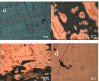
Fig. 1. Optical microscope images of Cu foil after heating for (a) 5 min, (b) 10 min, (c) 15 min, and (d) 20 min.
annealing time was set to 1 and 5 min. Fe foils were heated at temperatures of 600, 650, 700, and 750 °C for 1 min. In addition, we used Fe thin films formed on a Si (001) surface as a substrate. For the preparation, Si(001) substrates were cleaned in ethanol via ultrasonic cleaning, and, subsequently, Fe thin films 100 nm in thickness were deposited on these substrates. For the graphite growth, these substrates were annealed at a temperature from 600 to 750 °C for 1 min. After the annealing process, the samples were analyzed using micro Raman spectroscopy. The wavelength of the excitation laser was 532 nm and 785 nm for the measurements of Ni and Fe and Cu, respectively. To calculate the coverage of the amorphous carbon from an optical image, we used the free software “Image J”3).
3. RESULTS AND DISCUSSION
3.1 Growth on the Cu Foil After annealing in the furnace, we analyzed the products on the sample surfaces using the Raman microscope. Figure 1 shows optical-microscope images of the sample surface of the Cu foils after annealing at 950 °C for from 5 to 20 mins. Gray and orange areas were found on these images
Fig 2. Raman spectrum captured from the center of the images of Fig. 1a (top) and 1d (bottom).
Fig. 3. Annealing time vs. coverage of amorphous carbon for a substrate temperature of 900 and 950 °C.
and the area of the grayportion contracted with increasing annealing time. In each area, Raman spectra were captured and typical spectra are shown in Fig. 2. The Raman spectrum captured from the center of the image of Fig. 1(a), which is a typical result of the gray area, is shown in the top spectrum in Fig. 2. In this spectrum, two peaks, which can be attributed to the G and D bands, were respectively found at 1607 cm-1 and 1357 cm-1. These peaks
are very close while at approximately 2700 cm-1, where the 2D
peak should appear, no peak was observed, indicating that amorphous carbon (a mixture of sp3 and sp2)4) thin films covered
the gray area. The bottom spectrum in Fig. 2 was captured at the center of Fig. 1(d), which is a typical spectrum for the orange area. In this spectrum, no peak can be found except for a broad undulation, which could be caused by the background correction of the spectrum for the fluorescence and does not have any significance. Because carbon material covered the surface, some peaks such as the G and D bands appear such as the top spectrum, meaning that carbon material disappeared from this orange area. From the images shown in Fig. 1, we found that the gray area contracted and the orange area expanded, indicating that the carbon atoms migrate and disappear from the surface with increasing annealing time.
From the optical images shown in Fig. 1, the gray area occupancies in the images, which correspond to the coverage of the amorphous carbon, were calculated and summarized as shown in Fig. 3. The similar results obtained from samples annealed at 900 °C are also shown. When these data are plotted at a semi-logarithmic scale, the data are linearly aligned, indicating the data exponentially changes. From the semi-logarithm plot, we obtained a time constant, and then, calculated the reaction
Table 1. Time constants and reaction velocities corresponding to annealing temperatures for the Arrhenius plot.
T (°C) 1/T (K-1) t (min) k (s) Log e(k) 900 0.000852 17.18 0.000969 -6.94 950 0.000818 8.92 0.001873 -6.28 0 500 1000 1500 2000 2500 3000 In ten si ty (a rb .u n it s) (c ps ) Raman Shift(cm-1) amorphous carbon Cu C 0 20 40 60 80 100 0 5 10 15 20 C ov er ag e (%)
Time (min)
900 ℃ 950 ℃c
d
a
b
Fig 4. Arrhenius plot of the coverage (the logarithm of the reaction velocity vs. the inverse of the substrate temperatures).
velocities. These results are summarized in Table 1. From these data, an Arrhenius plot was obtained as shown in Fig. 4. The following is the Arrhenius equation:
𝑘 = 𝐴exp −!!
!" (1)
where k, A, Ea, R, and T are, respectively, the reaction velocity,
pre-exponential factor, activation energy, gas constant, and substrate temperature. Considering this equation, the slope of the line, m, can be described by the following formula:
𝑚 = −!!
! (2).
From Fig. 4, the value of -1.89 × 10⁴ was obtained for m, and then
the activation energy was calculated as 157 kJ/mol, corresponding to 1.63 eV. Here, the gas constant value, R = 8.314 J/mol•K, was used. The activation energy of the surface diffusion on the Cu surface is 0.07 eV5) and that of the oxidation of carbon is 110.5
and 393.5 kJ, for CO and CO2, respectively6). The activation
energy obtained from our experimental results differed from these values. At the least, we can conclude that the rate limiting reaction does not correspond to these two processes. Another candidate for the process related to the disappearance from the surface of the Cu foil is diffusion through crystal grain boundaries; the other process is difficult to image in this case. Therefore, we believe that the carbon atoms disappear though the grain boundaries and that graphene could not be grown in this case.
3.2 Growth on the Ni foil Raman spectra captured after
annealing at temperatures from 600 to 700 °C are shown in Fig. 5. We found D and G peaks, respectively, at 1335 and 1590 cm-1. In
the spectrum of 600 °C, the 2D band was not found, indicating that the product is amorphous carbon. Meanwhile, in the spectrum of 650 °C, we found G, D, and 2D peaks, respectively, at 1626,
Fig 5. Raman spectrum of the Ni surface heated at a temperature from 600 to 700 °C. For 700 °C the spectrum for the heating time of 5 min is also shown.
1431, and 2681 cm-1. The intensity of the G band peak was higher
than that of the 2D band, indicating that a graphene multilayer formed on the surface. A similar spectrum was obtained in the case of annealing at a temperature of 700 °C for 1 min. The G, D, and 2D peaks were at 1631, 1375, and 2683 cm-1, respectively. At
an annealing temperature of 700 °C, we attempted to anneal for 5 mins. We found very weak peaks of the D and G bands at 1415 and 1671 cm-1, respectively, and scarcely found a 2D peak,
indicating that surface carbon barely remained. A small peak was observed at 1100 cm-1,1500 cm-1 indicating that a nickel oxide
layer7) formed. These results indicate that graphite formed at
650 °C and 700 °C although a certain amount of amorphous carbon remained on the surface. Further annealing above 700 °C for 5 mins caused the carbon layer on the surface to disappear while a nickel oxide layer appeared, which would be an initial surface before the deposition of the amorphous carbon.
To estimate the graphite quality, the full widths at half maximum (FWHM) of the 2D band peaks were calculated by the fit of the Raman spectra shown in Fig. 5, in which a Lorentzian function was used. The spectra of the original data (dots) and the curves of the fit (line) are shown in Fig. 6 for 650 and 700 °C. From the fit, we obtained the FWHM values of the 2D peaks
Fig. 6. 2D band spectra of (a) 650 °C and (b) 700 °C and the results of the peak fit for calculating the full width at half maximum.
-7
-6.8
-6.6
-6.4
-6.2
-6
8.00
8.20
8.40
8.60
log
ek (
k:
R
ea
ct
io
n
ve
lo
ci
ty)
1/T (10
-4/K)
0 1000 2000 3000 In ten si ty (a rb .u n it s) (c ps ) Raman Shift (cm-1) 0 600 ℃ 700 ℃ (1 min) 700℃ (5min) 650 °C (a) (b)Supissara RUANGWIT, Fumihiko MAEDA
Table 2. Full width at half maximum of the 2D peak and intensity ratio of the G band peak to the D band peak obtained from analyses of the Raman spectrum shown in Fig. 5.
Temperature (°C) 650 700
FWHM (cm-1) 75.01 81.79
G/D ratio 1.04 0.90
indicated in Table 2. The peak intensity ratios of IG/ID of the
spectra shown in Fig. 5 are also shown in this table. In Fig. 5, the envelope of the peaks of the G and D bands and the ratios of IG/ID
are very similar to the amorphous carbon (sp2), and most of the
carbon is amorphous carbon (sp2). However, we found 2D peaks
at 650 °C and 700 °C although the intensities of the 2D peaks were much smaller than those of the G band peaks. These results indicate that the products are a mixture of graphite and sp2-amorphous carbon. In addition, the FWHMs of the 2D peaks
are significantly larger than those of the graphite grown on Fe thin films described later, indicating the quality of the graphite is significantly worse although graphite was grown on these Ni foils.
3.3. Growth on the Fe foil Raman spectra captured from
the surface of the Fe foils after samples were annealed at 600, 650, and 700 °C for 1 min are shown in Fig. 7. In the spectra at 600 and 700 °C, several peaks are observed between 228 and 1319 cm-1,
which are attributed to Fe2O38). In addition, the peaks of the G and
2D bands are respectively found at 1589 and 2698 cm-1 at 600 °C and 1562 and 2676 cm-1 at 700 °C, while the peak of the D band is
not observed because there is a large peak of Fe2O3at 1319 cm-1.
Meanwhile, in the spectrum of the sample after annealing at a temperature of 650 °C, three peaks, the G, D, and 2D bands, were observed at 1620, 1389, and 2740 cm-1, respectively, while several peaks attributed to Fe3O48) were observed. In the cases of 600 and
700 °C, the iron oxide is Fe2O3 and the Gand 2D peaks are faint,
while in the case of 650 °C, the oxide is Fe3O4 and the intensities
of both peaks are small but far greater than those at 600 and 700 °C.
In any case, we found formation of graphite on the Fe foils, although the amount was small. Because, in all the Raman spectra shown in Fig.7, there are distinct peaks derived from iron oxide, we speculated that the small amount of graphite was caused by the thick surface oxide. Therefore, we conjectured that the situation could be improved if a vapor-deposited thin film was used as a substrate, because the thick oxide layer that forms on the Fe foil is caused by the rolling process. Hence, we used Fe thin films formed on a Si(001) substrate to grow more graphite as described below. From the viewpoint of the amount of graphite, the best result in the Fe foil cases for the three annealing temperatures was for 650 °C. This was because of the reduction reaction of the surface oxides from Fe2O3 to Fe3O4. However, it is not clear why
this reaction occurred only at this temperature and why Fe3O4 is
Fig 7. Raman spectra of the Fe foil after heating at (a) 600, (b) 650, and (c) 700 °C for 1 min.
more favorable for graphite growth than Fe2O3. Further study is
needed to understand this phenomenon.
3.4. Growth on Fe/Si(001) Amorphous carbon thin films
formed on the Fe thin films on the Si(001) which were annealed at varioustemperatures. Raman spectra of the samples are shown in Fig. 8. In the spectra of the samples annealed at temperatures from
Fig 8. Raman spectra of Fe foil of the surface heated at 600 °C, 650 °C, 700 °C, and 750 °C. -10 40 90 140 190 240 290 0 1000 2000 3000 In ten si ty (a rb .u n it s) (c ps ) Raman Shift (cm-1)
(a)
-10 10 30 50 70 90 110 0 500 1000 1500 2000 2500 3000 3500 In ten si ty (a rb .u n it s) (c ps ) Raman Shift (cm-1)D G
2D
-10 90 190 290 0 1000 2000 3000 4000 Int ens it y (a rb.uni ts ) (c ps ) Raman Shift (cm-1)G 2D
(c)
0 500 1000 1500 2000 2500 3000 3500 Int ens it y (a rb.uni ts ) (c ps )Raman Shift (cm
-1)
600 ℃ 650 ℃ 700 ℃ 750 ℃ 1000 2000 3000 1500 2500G
2D
Fe2O3 1000 1600 2200 2800 (b) Fe2O3 Fe3O4 Fe 3O 4 Si 3FeO 4 Si
Fig 9. 2D band spectra of (a) 600 (b) 650 and (c) 700 °C and results of peak fit for calculating the FWHM.
600 to 700 °C, we found the G, D, and 2D peaks, respectively, at 1593, 1343, and 2698 cm-1, while these peaks were not found in
the spectrum at 750 °C. Furthermore, in all spectra, at the region lower than 800 cm-1, several peaks attributed to Fe
3O4 were
observed and peaks attributed to the Si substrate were observed at 520 and 1000 cm-1. These results indicate that graphite formed
when the samples were annealed below 700 °C but not at 750 °C. When annealing above 700 °C, the native Si oxide layer at the interface between the Fe thin film and Si substrate disappeared and an iron silicide started to form9). Hence, when annealing at
750 °C, we speculate that iron did not remain at the sample surface which prevented graphite growth. This speculation is consistent with the intense Si peak observed in the spectrum at 750 °C and suggests that graphite cannot grow on this structure above 700 °C.
To examine the domain size and number of graphene layers, we analyzed the graphite related peaks shown in Fig. 8. For the analysis of the 2D peaks, the Lorentzian function was used to fit the spectra. In Fig. 9, the fitting curves (line) together with the original data (dots) are indicated for 600, 650, and 700 °C. From the fit, we obtained the values of the (FWHM)of the peaks indicated in Table 3. The peak-intensity ratios of IG/I2D and IG/ID
and the domain sizes calculated from IG/ID10) are also indicated
in Table 3. We can estimate the number of layers from the IG/I2D
ratio. The values are greater than two, indicating that the number of graphene layers is greater than three11).In addition, we found
that all 2D peaks shown in Fig. 9 are symmetric. These results
indicate that the graphite obtained in this case is multilayer turbostratic graphene12). In Table 3, the higher annealing
temperature corresponds to a larger domain size, indicating that the quality of the graphene improved. Hence, at 700 °C, the graphite shows the best quality in our experiment.
Meanwhile, when the Raman spectra in Fig. 8 are compared to those in Fig. 7, the peak intensity of the G band in Fig. 8 is much higher and more prominent than that shown in Fig. 7, indicating that the amount of graphite grown on the Fe/Si is greater than that on the Fe foils. In addition, the FWHM of the G band at 700 °C
Table 3. FWHMs of the 2D band obtained from the fit shown in Fig. 9, the intensity ratios of IG/ID and IG/I2D, and the domain size calculated from the
IG/ID obtained from the analyses of the Raman spectra at 600, 650, and
700 °C for Fe/Si(001). Temperature (°C) 600 650 700 FWHM (cm-1) 80.92 60.06 54.74 G/2D ratio 5.93 2.31 2.05 G/D ratio 1.03 1.04 1.33 Domain size (nm) 10.25 10.29 11.65
shown in Fig. 8 is obviously smaller than that shown in Fig. 7(b), indicating higher crystallinity. In contrast, the peak intensity of the peaks related to Fe3O4 shown in Fig. 7(b) is much higher than that
of Fig. 8. This shows that the thickness of the iron oxides of the Fe/Si is thinner than that of the Fe foils. From these results, we can conclude that the growth of graphite improved via the use of Fe thin films formed on the Si substrates instead of the Fe foils because of the formation of a thinner iron oxide layer.
3.5. Discussion On the Ni and Fe foils, graphite formed on
the surfaces although the amount was small and the quality low. In the case of Cu foil, the amorphous carbon thin film merely disappeared without the reaction with the substrate and graphene/graphite was not found on the surface (Figs. 1 and 2). We interpreted that these differences were caused by the difference in the carbon-solubility of the substrates. Meanwhile, the activation energy derived from the annealing temperature dependence of the coverage of amorphous carbon on the Cu surfaces suggests that the path of the carbon atoms in their disappear from the surface is migration though crystal grain boundaries.
Considering these results, we can interpret that both reactions, carbon solution into the foil substrates and absorption into the crystal boundaries after surface migration during annealing, simultaneously occur. Because the solid solubility of carbon into the Cu is fairly low, the main disappearance path of the carbon atom is the latter reaction, resulting in amorphous carbon remaining on the surface at a higher temperature than that of the Ni and Fe foils. In the case of the Ni and Fe foils, because both reactions were comparable and simultaneously occur, the amorphous carbon thin films disappear at a relatively lower temperature. We believe that this difference resulted in the formation of the graphite on the Ni and Fe foil surfaces but not on the Cu foil surfaces.
Meanwhile, in the case of the Fe foils, distinct peaks derived from iron oxides were observed in the Raman spectra after annealing while graphite-related peaks were also observed (Fig. 7), indicating that carbon atoms can dissolve into the substrate during annealing and segregate from it during the cooling process even though a thick oxide layer formed. Because the surface of the Ni and Cu is not inert to avoid surface oxidation, an oxide layer could
(a) (b)
Supissara RUANGWIT, Fumihiko MAEDA form on the surface to varying degrees. Thus, we believe that the
surface oxide layer enhanced surface migration of the carbon atoms and disturbed the solid solution of carbon atoms, resulting in the suppression of graphite formation.
Hence, we suppose that the solution and segregation reaction effectively occurred and, that more graphite could be obtained, if the oxide layer was thinner than that on the foils used during these experiments. Then, we attempted to grow graphite on Fe thin film formed by evaporation on the Si (001) substrate because the thickness of the oxide layer was thinner and more graphite of higher quality than that formed on the Fe foils was obtained.
The aforementioned discussion provided the following insight into the surface reaction during the heating process: Because of the manufacturing process and the long time following production, thick oxide layer would form at the surface on the foil, and the oxide layer suppressed the solid solution of carbon. Therefore, because our method does not involve removal of the surface oxide before carbon thin film deposition, the amount of graphite grown on the surface is small. However, when the thickness of the surface oxide layer is sufficiently thin, a significant amount of graphite can be grown such as on the Fe thin film formed by evaporation. If we can successively conduct surface cleaning and carbon deposition without exposure to air, we do not have to consider this problem. However, such a process increases the production cost. Our results show the possibility of the formation of high-quality graphene on basis of thickness control of the surface oxide layer. This information is beneficial to low-cost production of graphene.
4. CONCLUSIONS
We studied graphene growth using amorphous carbon thin film using a simple method in which carbon thin film was deposited on metal substrates prior to growth instead of flowing raw material gas during growth in the conventional CVD method. This is the first systematic study to investigate the growth mechanism of the proposed graphene-producing method.
First, we examined the growth using Ni, Fe, and Cu foils which are typical substrates for CVD growth of graphene. In the case of the Cu foil, we did not obtain graphene/graphite when the samples were annealed at 900 and 950 °C, while one area of the surface was covered with amorphous carbon thin film but no carbon was observed in the other areas. The ratio of these areas was in accordance with the annealing time and a longer annealing caused disappearance of carbon atoms. However, on the Ni and Fe foils, graphite formed on the surface when the substrate was annealed at a temperature from 600 to 700 °C whereas a longer annealing also caused disappearance of carbon atoms. Furthermore, in the case of the Fe foil, Fe oxide was observed on the surface using Raman spectroscopy. These results suggest that carbon solution into the
foil substrates and absorption into the crystal boundaries after surface migration during annealing simultaneously occur and that the fairly low solid solubility of carbon into the Cu suppressed graphite formation.
Then, because we suspected that the thick oxide layer disturbs the formation of graphite from this examination, Fe thin film deposited on the Si (001) substrate was used instead of Fe foils for growth. As a result, the oxide layer was thinner and more graphite of higher quality than that formed on the Fe foil, were obtained. This result supports our interpretation. Moreover, our result suggests that the thickness of the oxide layer is essential in growing graphene on metal with high carbon solubility and that the migration of carbon through the crystal boundaries is key factor in growth.
ACKNOWLEDGEMENTS
We would like to thank Prof. S. Tanaka of the Fukuoka Institute of Technology for his aid in preparing the Fe thin film on the Si substrate using the vacuum evaporation system. This work was partially supported by the Japan Society for the Promotion of Science Grants-in-Aid for Scientific Research KAKENHI Grant Number JP19K0527 and KAKENHI-Retry Grant 2018 of Electronics Laboratories in Fukuoka Institute of Technology .
(Received on October 18, 2019) References
1) Z. Sun, Z. Yan1, J. Yao, E. Beitler, Y. Zhu, and J.M. Tour, Nature 468, 549 (2010).
2) Z. Peng, Z. Yan, Z. Sun, and J.M. Tour., ACS Nano 5, 8241 (2011). 3) C.T. Rueden, J. Schindelin, and M.C. Hiner, et al. BMC Bioinformatics
18:529, PMID 29187165 (2017).
4) A.C. Ferrari and J. Robertson, Phys. Rev. B 64, 075414 (2001). 5) O.V. Yazyyev and A. Pasquarello, Phys. Rev. Lett. 100, 156102 (2008). 6) A. Theodosiou, A.N. Jones, B. Marsden, PLoS ONE 12(8), e0182860 (2017). 7) N. Mironova-Ulmane, A. Kuzmin, l. Slidos, and M. Pärs, Cent. Euro. J. Phys.
9, 1096 (2011).
8) T. Ohtsuka, Boshoku Gijutsu, 35, 352 (1986).
9) F. Maeda, H. Hibino, S. Suzuki, and F.Z. Guo, Surf. Interface Anal. 40, 1747 (2008).
10) M.M. Luschese, F. Stavale, E.H.M. Ferreira, C. Vilani, M.V.O Moutinho, B.C. Rodrigo, C.A. Achete, and A. Jorio, Carbon 48, 1592 (2010). 11) D. Graf, F. Molitor, K. Ensslin, C. Stampfer, A. Jungen, C. Hierold, and L.
Wirtz, Nano Lett. 7, 238 (2007).