Japan Advanced Institute of Science and Technology
JAIST Repository
https://dspace.jaist.ac.jp/
Title
容量‑周波数‑温度マッピングによるワイドキャップ金
属‑絶縁体‑半導体デバイスの解析手法
Author(s)
Shih, Hong‑An
CitationIssue Date
2014‑09
Type
Thesis or Dissertation
Text versionETD
URL
http://hdl.handle.net/10119/12308
RightsDescription
Supervisor:鈴木 寿一
Characterization method for wide-gap metal-insulator-semiconductor devices
by using capacitance-frequency-temperature mapping
Hong-An SHIH
Japan Advanced Institute of Science and Technology
DOCTORAL DISSERTATION
Characterization method for wide-gap metal-insulator-semiconductor devices
by using capacitance-frequency-temperature mapping
by
Hong-An SHIH
submitted to
Japan Advanced Institute of Science and Technology in partial fulfilment of the requirements
for degree of Doctor of Philosophy
Supervisor: Prof. Toshi-kazu SUZUKI, Ph.D.
School of Materials Science
Japan Advanced Institute of Science and Technology
September 2014
i
Abstract
Wide-gap semiconductor GaN is anticipated for its potential to overcome the trade-off relation between speed and power in semiconductor devices. In particular, GaN-based metal-insulator-semiconductor heterojunction field-effect transistors (MIS-HFETs) have been investigated extensively owing to the merits of gate leakage reduction and passiva- tion to suppress the current collapse. For both gate-insulator or passivation applications, controlling insulator-semiconductor interfaces is critical for device performances. There- fore, it is important to characterize and analyze the interface states. In fact, we observe frequency dispersion in C-V characteristics of MIS devices, attributed to electron trap- ping/detrapping at interface mid-gap states leading to gate-control impediment. Such mid-gap states in GaN-based devices have been characterized and analyzed by conduc- tance method, Terman method, photo-assisted C-V method, and deep level transient spectroscopy. Although the conductance method is widely used, there are difficulties in the analysis of deep interface states with long trapping time constants in MIS devices based on wide-bandgap materials like GaN. Also, the analysis results obtained from the conductance method is affected by the assumed value of the insulator capacitance.
In this work, we proposed and developed a method using capacitance-frequency- temperature (C-f-T) mapping obtained from the temperature-dependent C-V-f char- acteristics for GaN-based MIS devices, based on the Lehovec equivalent circuit. From constant-capacitance contours, exhibiting a straight line behavior in the mapping, an ac- tivation energy Ea corresponding to an interface state energy level can be extracted for a wide range of gate biases without assuming any parameter. The gate bias dependence of the activation energies leads to many insights into the MIS devices. The effectiveness of the method is exemplified by application to AlN/AlGaN/GaN MIS devices. Through characterizing the activation energies modulated by the gate biases, we can obtain the gate-control efficiency of the MIS devices, i.e., the ratio of the bandbending change in the semiconductor to the total gate voltage change. Even though the Lehovec equivalent circuit is based on an AC small-signal model, we find that its DC limit, described by the insulator capacitance, the semiconductor capacitance, and the interface state density, gives the gate-control efficiency. Therefore, we can evaluate the interface state density from the experimentally obtained gate-control efficiency, using the values of insulator and semiconductor capacitances. From the activation energies corresponding to a wide range of gate biases, we can obtain the gate-control efficiency and the interface state den- sity corresponding to deep interface states in comparison with the conductance method.
Moreover, it is shown that the gate-control efficiency and the interface state density have
ii
correlations with the linear-region intrinsic transconductance. In addition, we give char- acterization of the AlN-AlGaN interfaces by using X-ray photoelectron spectroscopy, in relation with the results of the analysis.
In summary, we have proposed and developed the C-f-T mapping method, a char- acterization method for wide-gap MIS devices. The method gives activation energies of electron trapping for a much extended range of gate biases, compared to the conventional conductance method. The effectiveness of the method is exemplified by applications to the AlN/AlGaN/GaN MIS devices, with evaluation of the gate-control efficiency, the interface state density, related to the intrinsic transconductance. The C-f-T mapping method provides the insights of deep interface states, being useful in the characterization of wide-gap MIS devices.
Keywords: wide-gap MIS devices, C-V characteristics, frequency dispersion, C-f-T mapping, interface states, AlGaN/GaN
CONTENTS iii
Contents
Abstract i
Contents iii
1 Introduction 1
1.1 Compound semiconductors and their applications . . . 1
1.2 GaN-based semiconductors and related devices . . . 4
1.3 Purpose of this study . . . 10
1.4 Organization of the dissertation . . . 11
2 Principle of characterization method using capacitance-frequency- temperature (C-f-T) mapping 13 2.1 Conventional conductance method . . . 13
2.2 A novel frequency domain characterization method —– C-f-T mapping method . . . 17
3 Application of C-f-T mapping method to AlN/AlGaN/GaN MIS de- vices 19 3.1 Device fabrication . . . 19
3.2 DC characterization . . . 33
3.3 Characterization by using C-f-T mapping method: A comparison with conventional conductance method . . . 35
3.4 Application ofC-f-T mapping method to device process comparison . . . 41
3.4.1 Gate-control efficiency and interface state density . . . 49
3.4.2 Relations with intrinsic transconductance . . . 53
3.4.3 Relations with X-ray photoelectron spectroscopy analysis . . . 57
4 Conclusion and future perspective 61 4.1 Conclusion . . . 61
4.2 Future perspective . . . 62 Appendix A Algorithm of obtaining contours in C-f-T mapping 63
Bibliography 67
List of publications 75
iv CONTENTS
Acknowledgements 79
1
Chapter 1 Introduction
1.1 Compound semiconductors and their applications
While silicon still dominates digital integration circuit applications, compound semi- conductors are playing increasingly important roles in a number of cutting-edge wireless- communication and power-switching applications. For high-speed wireless-communication applications, the demand for exchange of high-quality contents is escalating through vari- ous forms of communication devices including cell phone, television, and satellite commu- nications. The type of semiconductor material employed also depends on the speed and power requirements of each application. As shown in Fig. 1.1, cell phones in the mobile communication require a moderate frequency ∼ 1 GHz and a low output power ∼ 1 W, while a ∼ 100 W capability is necessary for base stations [1]. For satellite broadcasting, even higher frequency and output power are required. In the present time, Si-LDMOSFET (laterally diffused metal-oxide-semiconductor field-effect transistor) [2], GaAs-HBT (het- erojunction bipolar transistor) [3], GaAs-HFET (heterojunction FET) [4], InP-HFET [5], and vacuum tube are employed for these applications according to the speed and power re- quirements. Realization of high-speed and high-power devices that function at frequency range from a few GHz to 100 GHz is a milestone for the future wireless communica- tion system [6]. For power-switching applications shown in Fig. 1.2 [7], the frequency range is downscaled by 105 orders while the power range is upscaled by the similar or- ders, compared to those of the wireless-communication applications. The main role of the semiconductor devices in these applications is to handle the actual power consumed during operation. Hence the capability to handle a large power is a criterion. Depending on application, a moderate switching speed is sometimes required. Si-based materials have been employed for such device purposes. However, owing to the physical limits of Si-based materials, the energy loss during operation is a major issue. It should be noted that there is a trade-off relation between speed and power for both applications.
To understand this trade-off relation, we shall look into the physical properties of semiconductors employed for electronic devices such as field-effect transistors (FETs).
First, as an indicator of the device speed, current-gain cut-off frequency fT is employed, which can be expressed as
fT ' 1
2πτtr = v
2πLG, (1.1)
2 Chapter 1 Introduction
RF power [W]
Frequency [GHz]
GaAs SiC
Si
SiGe
III-N
professional-use wireless
digital cellular
digital cordless phone
automotive radar
0.5 1 2 5 10 20 50 100
1 100
10 1k
0.1
analog cellular cellular base station broadcast
microwave oven
ITSETC WLLWLAN
VSAT BS
CS satellite
broadcasting
LMDS P-MP WLAN phased
array radar
FIG. 1.1 Power and frequency in communication systems and related semiconductors [1].
FIG. 1.2 Power and frequency in power-switching systems and related semiconductors [7].
where τtr is the transition time, v is the carrier velocity, and LG is the gate length. fT is the cutoff frequency at which the current gain equals to 1. From Eq. 1.1, it is obvious that a high velocity and a short gate length increase fT. Up to present days, shrinkage of the gate length has led to continuous improvement of device performance. However, it is pushing the physical limit of Si systems. We have to look into the physical properties of other semiconductor materials with a high carrier velocity. Regarding the carrier velocity, mobility µat low electric field and saturation velocity vsat at high electric field should be taken into consideration. The mobility µ is expressed as
µ= qτ
m∗, (1.2)
where q is the electron charge, m∗ is the electron effective mass, and τ is the momentum
1.1 Compound semiconductors and their applications 3
relaxation time. On the other hand, vsat is given by vsat ∼
r~ωop
m∗ , (1.3)
where ~ωop is the optical phonon energy. This process is explained as below. By a given electric field, carriers are accelerated to gain a certain amount of energy. At a high field, when the energy of the carriers reaches ~ωop, a phonon is emitted and the carrier velocity drops to zero. Repeating this process, the carrier velocity reaches the saturation velocity vsat under an electric field. The common part of Eq. 1.2 and Eq. 1.3 is that they both have m∗ in the denominators. Therefore, a small m∗ is advantageous for the increase ofµandvsat. For the power-handling aspect of FETs, increasing the source-drain voltage is effective to obtain a high power. However, owing to the shrinkage of the gate length, the electric field under the gate becomes stronger leading to the limitation of the applicable voltage range, considering the breakdown field of semiconductors. Therefore, semiconductors with high breakdown field is advantageous for high-power applications.
The breakdown fields of semiconductors usually follow the relation
EB ∝Egα (α '1-3), (1.4)
which is a monotone increasing function of the energy bandgap Eg [8]. It is obvious that wide-gap semiconductor materials are advantageous for high-power applications. From the above discussion, we can conclude that small m∗ and large Eg are advantageous for high-speed and high-power applications, respectively. However, large Eg materials with small lattice constants usually have large electron effective mass m∗e, i.e.,
m∗e ∝Eg, (1.5)
unfavorable for the improvement of µ and vsat. For these reasons, a trade-off between speed and power exists in general cases [9]; it is considered difficult to satisfy the two simultaneously. To overcome the current limitations on speed and power set by Si or GaAs, we need materials that have a higher vsat and a larger Eg. If we take a look again at Eq. 1.3, there is an optical phonon energy term in the numerator indicating that wide-gap semiconductors possessing a large ~ωop may be available for high-speed and high-power device applications. GaN holds such physical properties giving possibilities to overcome the trade-off relation between speed and power.
4 Chapter 1 Introduction
1.2 GaN-based semiconductors and related devices
Most of the compound semiconductor device technologies are restricted by crystalline growth quality; lattice-mismatch with substrates leads to crystalline defects in device layers, unfavorable for the device performance. One of the major obstacles for high-quality GaN growth is the lack of a suitable lattice-matched substrate. Low temperature growth of a buffer layer possessing 16 % lattice-mismatch with sapphire substrate was realized by MOVPE(metal organic vapor phase epitaxy) [13]. The maturity of this technology has now made the crystal growth quality of GaN, AlN, InN, or their alloys, to the production level. III-group nitride semiconductors are commonly in Wurtzite crystal structure and
0 1 2 3 4 5 6 7
3.0 3.2 3.4 3.6
Energy bandgap [eV]
Lattice constant (W, a−axis) [Å]
AlN
GaN
InN
0.0 0.5 1.0 1.5 2.0 2.5 3.0
5.2 5.4 5.6 5.8 6.0 6.2 6.4 6.6
Energy bandgap [eV]
Lattice constant (ZB) [Å]
Si
Ge GaAs
AlAs
InAs AlP
GaP
InP
AlSb
GaSb
InSb
FIG. 1.3 Relation of energy gap and lattice constant in III-V compound semiconductors [10,11].
0.00 0.05 0.10 0.15 0.20 0.25
0.0 0.5 1.0 1.5 2.0 2.5 3.0 3.5 4.0 Electron effective mass, m
Γ/ m
0Energy bandgap, E
g[eV]
GaN
GaAs InAs GaSb
InSb GaN InGaAs InGaSb
FIG. 1.4 Relation of electron effective mass at Γ point and energy band gap.
1.2 GaN-based semiconductors and related devices 5
FIG. 1.5 Band structure of Wurtzite GaN [12].
are of direct bandgap materials. In principle, optical device applications are available from infra-red to ultra-violet region covered by the bandgaps of InN and AlN between 0.75 eV to 6.2 eV. In reality, green or blue light emitting diodes by InGaN are becoming more common in our daily life.
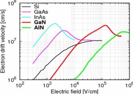
Figure 1.3 shows the relation between energy bandgap Eg and lattice constant a for III-V compound semiconductors. GaN has a small lattice constant with a large Eg ∼3.4 eV leading to a very high breakdown field of 3.3×10⁶ V/cm, favorable for high-power applications. However, from the relation between energy bandgap and electron effective mass shown in Fig. 1.4, it also has a large electron effective mass, unfavorable for high- speed device operation. As described earlier, high channel carrier velocity, which can be achieved by a large optical phonon energy or a small electron effective mass, is necessary for high-speed operation of FET. Despite the large electron effective mass, GaN has a small lattice constant with strong atomic bond energy that leads to a large optical phonon energy '90 meV. Also with a large valley-separation energy [12] shown in Fig. 1.5, GaN is anticipated to have a high saturation velocity. According to these properties, we obtain the electron transport properties of GaN by Monte Carlo simulation [14] as shown in Fig. 1.6. From the simulation result of the relation between electron drift velocity and electric field, it shows that GaN possesses ≥ 2.5×107 cm/s for electron peak velocity and ≥ 1.5×107 cm/s for electron saturation velocity, being an attractive material for electron transport. GaN possessing high saturation velocity and wide bandgap with high breakdown field, being attractive as the channel materials for high-speed and high-power electronic devices.
As a measure of suitability of a semiconductor material for high-speed and high-power transistor applications, we introduce two types of figure of merit (FoM) in the following.
Based on the physical properties given in Tab. 1.1, we make comparison between some major semiconductors. In Fig. 1.7, we show the relation of fT and the breakdown voltage
6 Chapter 1 Introduction
FIG. 1.6 Relation of drift velocity and electric field obtained by Monte Carlo simulation.
VB, given by
fTVB≤ EBvsat
2π , (1.6)
where the square of the right side of the equation is known as Johnson’s figure of merit [9]
determined by the intrinsic properties of the materials. It is obvious that GaN is much superior than Si and GaAs from the aspects of fT and VB. In Fig. 1.8, GaN-based HFET(HEMT) operated at freqency range ≥10 GHz and high-power output is expected to have wide applications such as power amplifiers for cellular base station, satellite com- munication, and automotive radar system [15–17].
Table 1.1 Physical properties of semiconductors [18, 19].
Mater. Bandgap Electron mobility Electron saturation Breakdown field [eV] [cm2/Vs] velocity [cm/s] [V/cm]
Si 1.12 1500 1.0 ×10⁷ 3.0 ×10⁵
GaAs 1.42 8500 2.0 ×10⁷ 4.0 ×10⁵
InAs 0.36 33000 ∼ 4.0 ×10⁷ 4.0 ×10⁴
SiC 3.33 900 2.0 ×10⁷ 3.0 ×10⁶
GaN 3.39 1100 2.7×10⁷ 3.3×10⁶
GaN-based III-V compound semiconductors also attract attentions as future power supply and switching devices. Such applications require moderate speed and higher power compared to those of wireless-communication applications. In Fig. 1.9, we show the relation of on-resistance Ron and breakdown voltageVB, given by
VB2
Ron ≤ ²µEB3
4 , (1.7)
where²µEB3 is known as Baliga’s figure of merit [20] determined by the intrinsic properties
1.2 GaN-based semiconductors and related devices 7
FIG. 1.7 Relation of fT and VB for several semiconductors.
FIG. 1.8 Power performance FOM(figure of merit) and applicable frequency range of device applications. By International Technology Roadmap for Semiconductors, 2005 Edi- tion [15].
of the materials. Here, we can also see the advantageous GaN with relatively low Ron
at high VB, being valuable for power electronics applications. Power electronics like Si- based vertical type MOSFETs used in power supply of server or personal computers, and Si-IGBT(insulated gate bipolar transistor) used in electric vehicle or hybrid cars, are expected to see appearance of GaN-based semiconductors [21], featuring both low on-resistance and high breakdown voltage with fast switching for substantial reduction of conduction and switching losses.
From the above discussion, GaN is expected to break through the trade-off relation in realization of high-speed and high-power electronic devices. Furthermore, it is possi- ble for GaN to form heterojunction with heterogeneous material AlGaN for high-speed
8 Chapter 1 Introduction
FIG. 1.9 Relation of Ron andVB for several semiconductors.
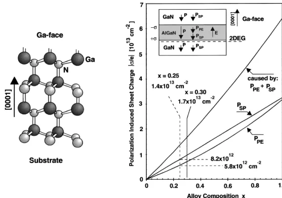
FIG. 1.10 Left: schematic drawing of the crystal structure of Wurtzite Ga-face GaN. Right:
calculated sheet charge density caused by spontaneous and piezoelectric polarization of a GaN-face GaN/AlGaN/GaN heterostructure. [22]
operation. AlGaN is grown pseudomorphically with a tensile strain to match the lateral lattice constant of Ga-face GaN. The Ga polarity is used to form a two-dimensional elec-
1.2 GaN-based semiconductors and related devices 9
FIG. 1.11 Illustration of gate leakage reduction and passivation in AlGaN/GaN MIS-HFETs.
FIG. 1.12 Illustration of gate leakage current and interface states in AlGaN/GaN MIS-HFETs.
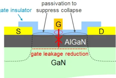
tron gas (2DEG) with high sheet carrier concentration by spontaneous and piezoelectric polarization at the AlGaN/GaN heterointerface as shown in Fig. 1.10 [22]. The concen- tration of 2DEG depends on the composition of III group materials and film thickness of AlGaN. Typically, Al composition of 20-30 % gives a 2DEG concentration '1013 cm−2. AlGaN/GaN heterojunction field-effect transistors [23] have been extensively developed as promising devices for high-speed and high-power applications. However, from the early stage of the development, AlGaN/GaN Schottky gate HFETs have been suffering from severe gate leakage current and current collapse. In order to solve these problems, AlGaN/GaN metal-insulator-semiconductor heterojunction field-effect transistors (MIS- HFETs) illustrated in Fig. 1.11, enabling effective reduction of the gate leakage current and current collapse, have been developed and studied. As a gate-insulator of the MIS de- vices, high-dielectric-constant (high-k) oxide materials, such as Al2O3 [24], HfO2 [25, 26], and also high-k nitride materials, such as AlN [27–31], BN [32,33], have been investigated.
Owing to their high thermal conductivities, the nitride materials are favorable also for pas- sivation of GaN-based devices, exhibiting good heat release properties [27, 34–38]. Since controlling insulator-semiconductor interfaces is critical for both gate-insulator or passi-
10 Chapter 1 Introduction vation applications, it is important to characterize and analyze the interface states. In fact, we observe frequency dispersion inC-V characteristics of MIS devices, attributed to electron trapping/detrapping at interface mid-gap states illustrated in Fig. 1.12, leading to gate-control impediment. Such mid-gap states in GaN-based devices have been char- acterized and analyzed by conductance method [28, 29, 39–44], Terman method [45, 46], photo-assisted C-V method [47, 48], and deep level transient spectroscopy [49–52]. Al- though the conductance method is widely used, there are difficulties in the analysis of deep interface states with long trapping time constants [53] in MIS devices based on wide-bandgap materials like GaN [29,30,54]. Also, the analysis results obtained from the conductance method is affected by the assumed value of the insulator capacitance.
In this work, we proposed and developed a method using capacitance-frequency- temperature (C-f-T) mapping [30, 55] obtained from the temperature-dependent C-V-f characteristics for GaN-based MIS devices, based on the Lehovec equivalent circuit [56].
From constant-capacitance contours, exhibiting a straight line behavior in the mapping, an activation energy Ea corresponding to an interface state energy level can be extracted for a wide range of gate biases without assuming any parameter. The gate bias dependence of the activation energies leads to many insights into the MIS devices. The effectiveness of the method is exemplified by application to AlN/AlGaN/GaN MIS devices. Through characterizing the activation energies modulated by the gate biases, we can obtain the gate-control efficiency of the MIS devices, i.e., the ratio of the bandbending change in the semiconductor to the total gate voltage change. Even though the Lehovec equivalent circuit is based on an AC small-signal model, we find that its DC limit, described by the insulator capacitance, the semiconductor capacitance, and the interface state density, gives the gate-control efficiency. Therefore, we can evaluate the interface state density from the experimentally obtained gate-control efficiency, using the values of insulator and semiconductor capacitances. From the activation energies corresponding to a wide range of gate biases, we can obtain the gate-control efficiency and the interface state den- sity corresponding to deep interface states in comparison with the conductance method.
Moreover, it is shown that the gate-control efficiency and the interface state density have correlations with the linear-region intrinsic transconductance. In addition, we give char- acterization of the AlN-AlGaN interfaces by using X-ray photoelectron spectroscopy, in relation with the results of the analysis.
1.3 Purpose of this study
We proposed and developed an analysis method for GaN-based MIS devices by using C-f-T mapping to evaluate the gate-control efficiency and the interface state density, both exhibiting correlations with the linear-region intrinsic transconductance. The effectiveness of the method is exemplified by application to AlN/AlGaN/GaN MIS devices to elucidate the properties of AlN-AlGaN interfaces depending on their formation processes. Using the C-f-T mapping, we extract the gate-bias-dependent activation energy with its derivative giving the gate-control efficiency, from which we evaluate the AlN-AlGaN interface state density through the Lehovec equivalent circuit in the DC limit. It is shown that the gate-
1.4 Organization of the dissertation 11 control efficiency and the interface state density have correlations with the linear-region intrinsic transconductance, all depending on the interface formation processes. The C- f-T method gives activation energies of electron trapping for a much extended range of gate biases, compared to the conventional conductance method. The method provides the insights of deep interface states, being useful in the characterization of wide-gap MIS devices.
1.4 Organization of the dissertation
Chapter 1:
Introduction of this research including the general background on compound semi- conductors, the GaN-based semiconductors and related devices, and the purpose of this work are given.
Chapter 2:
Explanation of the principle of characterization method using C-f-T mapping
Chapter 3:
Application of C-f-T mapping method to AlN/AlGaN/GaN MIS devices is dis- cussed. Firstly, we show the fabrication of the MIS devices including the in- depth characterization of the AlN thin films followed by the DC characterization.
We then make comparison between the analysis results of that by the conduc- tance method and the C-f-T mapping method. Furthermore, we discuss the gate- control efficiency and the interface state density characterized by theC-f-T mapping method. The effectiveness of the method is then demonstrated through the analy- sis of AlN/AlGaN/GaN MIS devices with different treatments for the AlN/AlGaN interfaces. The relations between the gate-control efficiency, the interface state den- sity, and the intrinsic transconductance of the MIS devices are also discussed. Lastly, X-ray photoelectron spectroscopy analysis of AlN/AlGaN interfaces are investigated to explain the analysis results.
Chapter 4:
Conclusion and future perspective of this research are given.
13
Chapter 2
Principle of characterization method using capacitance-frequency-
temperature (C -f -T ) mapping
2.1 Conventional conductance method
FIG. 2.1 An interface state energy level in the band diagram of a MIS structure.
For the insulator-semiconductor interface of a MIS device, the electron occupation probability P at an interface state shown in Fig. 2.1 is given by a time-dependent rate equation
∂P
∂t =γ(1−P)n−αP, (2.1)
where n is the semiconductor electron density at the interface, and γ,α are proportional constants. If we use the P, n, and surface potential V each separated into its DC and AC components given by
P = P0+Peexp(jωt) (2.2)
n = n0+enexp(jωt) (2.3)
V = V0+Veexp(jωt), (2.4)
14
Chapter 2 Principle of characterization method using capacitance-frequency- temperature (C-f-T) mapping we can obtain
Pe' P0(1−P0) 1 +jωτ P0
e n
n0 = P0(1−P0) 1 +jωτ P0
qVe
kBT, (2.5)
where P0 is the Fermi-Dirac distribution using the Fermi level EF, and τ = 1
γn0 (2.6)
is the time constant. Using the interface state density Di(E), a function of energyE, the total small signal AC admittance owing to the interface states is expressed as
Yi = Gi+jCiω (2.7)
= jωq Ve
Z
Di(E)PedE (2.8)
= jωq2 kBT
Z Di(E)P0(1−P0)
1 +jωτ P0 dE (2.9)
= jωq2
Z Di(E) 1 +jωτ P0
µ
−dP0
dE
dE. (2.10)
For the low temperature limit, since −dP0/dE 'δ(E−EF), using Di(E =EF) and P0 = 1/2, the admittance becomes
Gi+jCiω ' jωq2Di(EF)
1 +jωτ /2 , (2.11)
where
Gi
ω = ωτ q2Di
2(1 +ω2τ2/4) (2.12)
and
Ci= q2Di
1 +ω2τ2/4. (2.13)
For a discrete interface state where
Di(E) = D0 δ(E−E0) (2.14)
(note that the units of Di(E) and D0 are different), the admittance is expressed as Gi+jCiω = jωq2D0
1 +jωτ P0(E0)
exp[(E0−EF)/kBT]
kBT(1 + exp[(E0 −EF)/kBT])2. (2.15) For the case EF =E0, the admittance becomes
Gi+jCiω = jωq2D0
4kBT(1 +jωτ /2) (EF =E0), (2.16) where
Gi
ω = ωτ q2D0
8kBT(1 +ω2τ2/4) (2.17)
and
Ci= q2D0
4kBT(1 +ω2τ2/4), (2.18) exhibits the same frequency dependence as that in Eqs. 2.11-2.13.
2.1 Conventional conductance method 15 For general continuous interface states, since P0(1−P0) only holds values near the Fermi level EF, using Di(E =EF), Eq. 2.10 can be approximated as
Gi+jCiω ' jωq2Di
Z 1
1 +jωτ P0 µ
−dP0 dE
dE. (2.19)
Taking the integration of P0 from 0 to 1, we can obtain [56]
Gi
ω = q2Diln(1 +ω2τ2)
2ωτ (2.20)
and
Ci= q2Diatan(ωτ)
ωτ , (2.21)
being the basis of the conductance method.
FIG. 2.2 The equivalent circuit of the MIS structure.
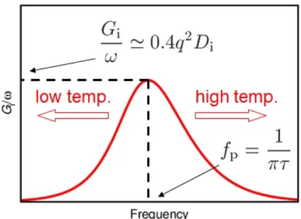
Based on the equivalent circuit of the MIS structures depicted in Fig. 2.2, with the in- sulator capacitanceC0, the semiconductor capacitanceCs, the interface state capacitance Ci, and the interface state conductance Gi, Gi/ω as a function of frequency exhibits a single-peaked behavior, with the peak frequency∼1/πτ and the peak value∼0.4q2Di, as illustrated in Fig. 2.3. Therefore, we can obtain time constantτ from the peak frequency.
From Eq. 2.6,
τ = 1 γn0
= 1
γNC
exp[β(EC−EF)] = τ0exp(βEa), (2.22) where n0 = NCexp[−β(EC −EF)] and τ0 = 1/(γNC), activation energy Ea can be ex- tracted from the Arrhenius plot of the temperature dependence of τ. However, accurate value of the insulator capacitanceC0 is required for this analysis, which may require extra experiments to determine theC0 value. Furthermore, owing to the much longer time con- stants corresponding to the deeper energy levels in wide-bandgap devices, it is sometimes difficult to obtain peaks in the measured frequency and temperature range. Assuming C0 = 600 nF/cm2, Cs = 300 nF/cm2, Di = 1014 cm−2eV−1, τ0 = 1 ns, and Ea = 0.5 eV, we obtain the calculation results shown in Fig. 2.4 based on the conductance method.
We have a problem that the peaks are obtained only for a narrow range of gate biases, prohibiting analysis of deeper interface states.
16
Chapter 2 Principle of characterization method using capacitance-frequency- temperature (C-f-T) mapping
FIG. 2.3 Illustration of a single-peaked behavior of Gi/ω as a function of frequency.
FIG. 2.4 Calculation results based on conductance method.
2.2 A novel frequency domain characterization method
—– C-f-T mapping method 17
2.2 A novel frequency domain characterization method
—– C -f -T mapping method
In order to solve the problem, we proposed an analysis method usingC-f-T mapping obtained from the temperature-dependent C-V-f characteristics. In Fig. 2.5, we show a C-f-T mapping with a contour, which is obtained by the numerical calculation with the same assumption as that for the conductance method. The contour exhibits a straight line behavior, which can be explained by the equivalent circuit of the MIS structures with a total admittance
Y = 1 Z =
µ 1
jC0ω + 1
Gi+jCsω+jCiω
¶−1
. (2.23)
SinceCigiven by Eq. (2.21) andGi/ωby Eq. (2.20) are functions of onlyωτ, the measured capacitanceC = ImY /ωis a function of onlyωτ. Therefore, a contour inC-f-T mapping, i.e., C = constant leading to ωτ = 2πf τ = constant, exhibits a straight line behavior as expressed by f ∝1/τ ∝ exp(−βEa), from which the activation energy Ea corresponding to the interface state energy level can be extracted. Due to slow ωτ dependence of Eqs. (2.21) and (2.20), even though the frequency is far from the peak position ∼ 1/πτ, change in the C-f-T mapping is detectable. Figure 2.5 shows the calculation results of the C-f-T mapping using the above parameters. The white line corresponds to the peaks in the conductance method; we can confirm that it is difficult to observe peaks in this frequency and temperature range. On the other hand, it is easy to find contours in the mapping, e.g., the black line, exhibiting a straight line behavior and giving the activation energy. The C-f-T mapping method gives Ea for a much extended range of the gate biases, providing many insights into the MIS devices.
FIG. 2.5 Calculation results based on C-f-T mapping method.
19
Chapter 3
Application of C -f -T mapping
method to AlN/AlGaN/GaN MIS devices
3.1 Device fabrication
FIG. 3.1 An AlGaN/GaN heterostructure.
Device fabrication was carried out using an Al0.29Ga0.71N(25 nm)/GaN(3000 nm) het- erostructure shown in Fig. 3.1, obtained by metal-organic vapor phase epitaxy on sap- phire(0001). Hall measurements of the heterostructure show an as-grown electron mobility µ'1400 cm2/V-s and a sheet electron concentrationns '1.0×1013cm−2. The following device processes were performed in order
1. marker formation
2. Ohmic electrode formation 3. device isolation
4. gate insulator deposition 5. gate electrode formation
Figure 3.2 illustrates the process flow of MIS device fabrication.
20Chapter 3 Application of C-f-T mapping method to AlN/AlGaN/GaN MIS devices
FIG. 3.2 Process flow of MIS device fabrication.
Marker formation
The purpose of marker formation is to provide a reference when aligning the gate electrode relative to the source and drain electrodes. The process flow is shown in Tab. 3.3.
Table 3.1 Process of marker formation Processes Conditions
surface treatment acetone, methanol, DIW 3 min each O2 plasma ashing 50 Pa 10 W 4 min Semico-clean 5 min, DIW 3 min baking 110 3 min
resist coating LOL2000(3000 rpm 60 s), bake(180 180 s) TSMR-8900(4000 rpm 60 s), bake(110 90 s) patterning exposure ∼12 mW/cm2(405 nm) 6.2 s
development NMD-W(60 s), DIW (180 s) surface treatment O2 plasma ashing 50 Pa 10 W 10 s
Semico-clean 5 min, DIW 3 min deposition Ti/Au=10/150 nm
lift-off 1165(60 )
acetone, methanol, DIW 3 min each
We employed a double layer structure, a lift-off layer LOL2000 (Rohm & Haas) and a positive resist TSMR-8900 (TOKYO OHKA KOGYO), for patterning. Also, Au was selected owing to its stability with temperature and easy emission of secondary electron during SEM observation in electron beam lithography process. The Ti is serving as a glue between AlGaN and Au layer to enhance their adhesion. An example of the completed marker is shown in Fig. 3.3.
3.1 Device fabrication 21
FIG. 3.3 Ti/Au marker.
Ohmic electrode formation
The purpose of forming Ohmic contacts is to provide an Ohmic-like access between the metal contacts (source and drain contacts) and the AlGaN/GaN 2DEG channel. In order to obtain such electrical property, proper metal selection and high-temperature annealing are important. Utilizing the gettering effect of Ti/Al layer, N-vacancy is induced in AlGaN/GaN layer during annealing, which is known to behave like donors [57, 58]. As a result, n-AlGaN and n-GaN form Ohmic contacts between the metal contacts (source and drain contacts) and the AlGaN/GaN 2DEG channel. The following Ti/Au metals are to cover the reactive Al surface from oxidation and etching during wet processes. Ti functions as a glue for Al and Au to enhance their adhesion.
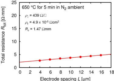
The Ohmic contact is evaluated by transmission line model (TLM) measurement.
Figure 3.4 shows an example of the TLM measurement result. The total resistance Rtot can be expressed as
Rtot '2Rc+R˜, (3.1)
where Rc is the contact resistance, and R˜ = ρ˜L is the sheet resistance given by the sheet resistivityρ˜and the electrode spacingL. From the intercept and gradient ofRtot-L relation, we can evaluate Rc and ρ˜, respectively.
FIG. 3.4 An example of TLM measurement results.
22Chapter 3 Application of C-f-T mapping method to AlN/AlGaN/GaN MIS devices
FIG. 3.5 Morphology of Ti/Al/Ti/Au after annealing at various temperatures for 5 minutes in N2 ambient.
The experiment for temperature-dependence of Rc was carried out to find the opti- mum annealing temperature giving the lowest Rc. Figure 3.2 shows the morphology of Ti/Al/Ti/Au after annealing at various temperatures for 5 minutes in N2 ambient. We can observe surface roughening due to the high temperature annealing as shown by the dull metal surfaces caused by irregular reflection.
The result of temperature dependence ofRcis shown in Fig. 3.6, in which 650shows the lowest Rc. This temperature is employed for Ohmic electrode formation as shown in the process flow described in Tab. 3.2.
3.1 Device fabrication 23
FIG. 3.6 Temperature dependence of contact resistance Rc.
Table 3.2 Process of Ohmic electrode formation Processes Conditions
surface treatment acetone, methanol, DIW 3 min each O2 plasma ashing 50 Pa 10 W 4 min Semico-clean 5 min, DIW 3 min baking 110 3 min
resist coating LOL2000(3000 rpm 60 s), bake(180 180 s) TSMR-8900(4000 rpm 60 s), bake(110 90 s) patterning exposure ∼12 mW/cm2(405 nm) 6.2 s
development NMD-W(60 s), DIW (180 s) surface treatment O2 plasma ashing 50 Pa 10 W 10 s
Semico-clean 5 min, DIW 3 min deposition Ti/Al/Ti/Au=10/200/100/50 nm lift-off 1165(60 )
acetone, methanol, DIW 3 min each annealing N2 atmosphere 650 5 min
24Chapter 3 Application of C-f-T mapping method to AlN/AlGaN/GaN MIS devices
Device isolation
FIG. 3.7 B+ concentration as a function of depth and acceleration voltage [59].
Implant isolation is a common method used in semiconductor device fabrication pro- cesses for inter-device isolation [60]. The generally applied ion implantation method causes damages in the semiconductor crystal, resulting the enhancement of electrical resistance in the defined area between the devices. It was reported that the implanted ion creates energy levels in or near mid-gap [61].
In our experiment, we employed LOL2000 and S1830 (Rohm & Haas) double layer for the ease of resist removal as the S1830 becomes impervious to resist remover 1165 (Shipley) after ion implantation. The patterning using the thick S1830 resist not only protects the device area but also defines the gate width. B+ ion from BF3gas was induced and implanted into the sample by acceleration voltages of 30 keV, 50 keV, and 100 keV.
The three-step implantation ensures uniform distribution of ions upto a certain depth in GaN from the AlGaN surface. Figure 3.7 obtained by SRIM/TRIM [59] simulator shows the B+ concentration distribution as functions of depth and acceleration voltage. It is shown that ∼300 nm from the AlGaN surface can be ion-implanted. The substitutional or interstitial B+ ion can cause Al, Ga, N vacancies which create deep levels that trap the carriers as illustrated in Fig. 3.8. As a result, the implanted area has high electrical resistance. Such deep levels can absorb and emit visible light with corresponding energy, causing the slightly yellowish look of the wafer after the ion implantation. The ion applied for implantation is not limited to B+only but also O+and Fe+are possible options [62,63]
Figure 3.9 shows the TLM results before and after the ion implantation. The latter shows the true sheet resistivity because the sheet resistance is correctly normalized by
3.1 Device fabrication 25 the defined gate width after the ion implantation. Device isolation process is described in Tab. 3.3.
FIG. 3.8 Deep levels created by ion implantation.
FIG. 3.9 TLM results before and after the isolation.
Table 3.3 Process of device isolation Processes Conditions
surface treatment acetone, methanol, DIW 3 min each O2 plasma ashing 50 Pa 10 W 4 min
resist coating LOL2000(3000 rpm 60 s), bake(180 180 s) S1830(4000 rpm 60 s), bake(110 90 s) patterning exposure ∼12 mW/cm2(405 nm) 30 s
development NMD-W(50 s), DIW(180 s) bake 140 5 min
ion implantation B+ 30 keV(1×1014 cm−2) + 50 keV(1×1014 cm−2) +100 keV(1×1014 cm−2)
resist removal 1165(60 ) + O2 plasma ashing 50 Pa 30 W 10 min
26Chapter 3 Application of C-f-T mapping method to AlN/AlGaN/GaN MIS devices
Gate insulator deposition
FIG. 3.10 Band lineup of GaN, AlGaN, and various insulators, including basic physical param- eters. [64–67]
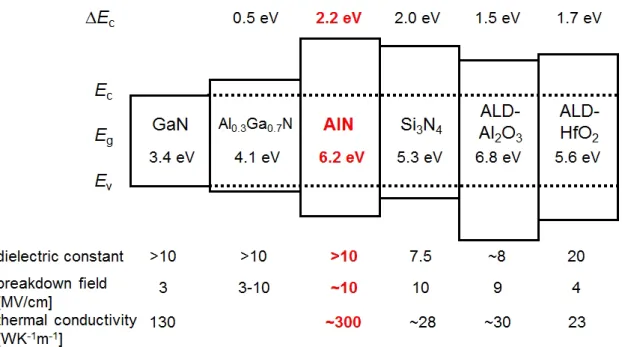
The gate insulator selection is critical for the device performance of MIS transistors.
The band lineup of GaN, AlGaN, and various insulators is shown in Fig. 3.10 [64–67].
In particular, high-dielectric-constant (high-k) oxide materials, such as Al2O3 [24] or HfO2 [25, 26], have been investigated as a gate dielectric insulator of the MIS transistors.
However, for such oxide insulators, there are difficulties in controlling the interface between the oxide and the nitride [68]. On the other hand, AlN is an important non-oxide high-k insulator, with a possible suitability for III-V device processing [69]. Previously, sputtering deposition of AlN on AlGaN/GaN, in which we expect a more controllable interface, was applied to passivation of AlGaN/GaN HFETs [27,34–37,70]. The AlN-passivated HFETs exhibit good heat release properties due to the high thermal conductivity of AlN [71]
(∼10 times higher than that of Al2O3), and also effective suppression of current collapse.
Since AlN has a possible high breakdown field >∼10 MV/cm [72,73] and a high dielectric constant∼10 [74], which are comparable to those of Al2O3, the sputtering-deposited AlN can be a favorable gate dielectric for AlGaN/GaN MIS transistors, with the merits of a more controllable interface and better heat release properties. Although AlGaN/GaN MIS transistors with a sputtering-deposited AlN gate dielectric [27, 28], as well as an AlN/GaN MIS-FET obtained by metal-organic vapor phase epitaxy (MOVPE) growth of AlN/GaN and regrowth of an n+-GaN Ohmic region [75], have been reported, sufficient device performance has not been shown, in particular, for forward gate leakage properties.
In this work, we carried out characterization of sputtering-deposited AlN films and their applications to AlGaN/GaN MIS transistors as a gate dielectric, including suppressed forward gate leakage properties [29].
3.1 Device fabrication 27
FIG. 3.11 Illustration of RF magnetron sputtering.
On the Al0.29Ga0.71N(25 nm)/GaN(3000 nm) heterostructure, AlN thin films were deposited at room temperature by RF magnetron sputtering using an AlN target in Ar-N2 ambient with a working pressure of 0.2 Pa and a plasma power of 40 W. The illustration of sputtering process is shown in Fig. 3.11. On the AlGaN surface cleaned by organic solvents, deionized water, and oxygen plasma ashing to remove surface organic contaminants, followed by oxide removal using Semicoclean (ammonium-based etchant), an AlN gate insulator of ∼19 nm thickness was deposited.
The AlN films do not show X-ray diffraction peaks in Fig. 3.12, suggesting their amorphous nature. In addition, by ellipsometry, we measured refractive indices of the AlN films obtained by this sputtering deposition condition. As shown in Fig. 3.13, a refractive index of 1.94 at 630 nm wavelength is obtained, indicating the dense nature of the deposited AlN films.
28Chapter 3 Application of C-f-T mapping method to AlN/AlGaN/GaN MIS devices
FIG. 3.12 XRD measurement of a sputtered AlN thin film.
FIG. 3.13 Ellipsometry measurement of a sputtered AlN thin film.
3.1 Device fabrication 29
FIG. 3.14 Al2p peak of an AlN film by XPS measurement.
FIG. 3.15 N1s electron energy loss spectroscopy of an AlN film by XPS measurement.
The AlN films have also been investigated by X-ray photoelectron spectroscopy (XPS) with a take-off angle of 35◦. Figure 3.14 shows an Al2p peak for an AlN film of ∼20 nm thickness. The Al2p signal is dominated by Al-N bonding, though the Al-O bonding was detected, which can be attributed to the residual oxygen in the film and the surface oxidation. Furthermore, the bandgap of the AlN was estimated by N1s electron energy loss spectroscopy, as shown in Fig. 3.15. We obtain the bandgap Eg ∼ 6.4 eV, which is similar to the literature value of 6.2 eV [76].
30Chapter 3 Application of C-f-T mapping method to AlN/AlGaN/GaN MIS devices
Gate electrode formation
Gate electrode formation uses a high resolution positive electron beam resist ZEP520A- 7 (ZEON Corp.). The single layer resist was employed without LOL2000 layer to prevent the etching of AlN insulator by the developer NMD-W (TOKYO OHKA KOGYO). Elec- tron Beam Lithography System (ELIONIX ELS-7500) supplies a 30 keV electron beam for patterning. Figure 3.16 shows the optical image of the gate electrode in completion. In Fig. 3.17, we show the SEM images; the MIS transistors have the gate length of 250 nm, the source-gate spacing of 2 µm, the gate-drain spacing of 3 µm, and the gate width of 50µm. For the MIS capacitors, the 100µm×100 µm gate electrode is surrounded by the Ohmic electrode as shown in Fig. 3.18. Gate electrode formation process is described in Tab. 3.4.
FIG. 3.16 Optical image of the gate electrode of the MIS transistor.
FIG. 3.17 Optical image of the gate electrode of the MIS transistor.
3.1 Device fabrication 31
FIG. 3.18 Optical image of the MIS capacitor.
Table 3.4 Process of gate electrode formation Processes Conditions
baking bake(180 5 min)
resist coating ZEP520-A7(4000 rpm 60 s), bake(120 180 s) Espacer(1500 rpm 60 s), bake(100 180 s)
patterning exposure (gate) 50 keV 50 pA pitch1 2.7 µs(∼135 µC/cm2) exposure (pad) 50 keV 50 pA pitch3 9.0µs(∼150 µC/cm2) Espacer removal: DIW(60 s)
development ZED-N50(60 s), ZMD-B(30 s), N2 blow surface treatment O2 plasma ashing 50 Pa 10 W 10 s
deposition Ni/Au=5/35 nm lift-off 1165(60 )
acetone, methanol, DIW 3 min each
32Chapter 3 Application of C-f-T mapping method to AlN/AlGaN/GaN MIS devices
Device dimensions
The completed MIS devices have dimensions shown in Fig. 3.19.
FIG. 3.19 Device dimensions of the fabricated MIS devices.
3.2 DC characterization 33
3.2 DC characterization
We carried out DC characterization for the fabricated AlN/AlGaN/GaN MIS devices.
In Fig. 3.20(top), we show the output characteristics of the fabricated MIS transistor, which exhibits no kink effect. Although we observed a slightly high on-resistance of
∼ 15 Ω · mm, a current drivability with a drain current of 550 mA/mm is obtained.
There is almost no negative conductance, suggesting good heat release properties. Fig- ure 3.20(bottom) shows the transfer characteristics under the gate voltage sweep of−18 V
→+6 V→ −18 V. According to the insertion of the AlN gate dielectric between the gate metal and the AlGaN, the transconductance is not so high; the maximum transconduc- tance is 100 mS/mm. Moreover, we observe a rapid decrease in the transconductance towards forward gate biases, suggesting poor AlN/AlGaN interface properties, which will be analyzed later. It should be noted that, owing to the good insulating properties of the AlN gate dielectric, the gate leakage currents are significantly small, 10−9 A/mm range or less, for both reverse and forward biases. The small leakage currents lead to the small drain off-currents, which exhibit more than 4 orders reduction in comparison with those of Schottky HFETs fabricated from the same AlGaN/GaN heterostructure.
FIG. 3.20 Output (top) and transfer (bottom) characteristics of the AlN/AlGaN/GaN MIS transistor.
34Chapter 3 Application of C-f-T mapping method to AlN/AlGaN/GaN MIS devices Figure 3.21 shows the gate-source two-terminal (drain open) I-V characteristics; we observe the gate current of 1 × 10⁻⁹ A/mm at a reverse voltage of −18 V, and 6 × 10⁻¹⁰ A/mm even at a forward voltage of +5 V, showing one of the most significant suppressions of forward gate leakage currents in AlGaN/GaN MIS transistors. Figure 3.22 shows the I-V characteristics of the fabricated MIS capacitor; we observe the current of 10−8 A/cm2 range for both forward and reverse biases.
FIG. 3.21 Gate-source two-terminal (drain open)I-V characteristics.
FIG. 3.22 I-V characteristics of the fabricated MIS capacitor.
3.3 Characterization by using C-f-T mapping method: A comparison with conventional
conductance method 35
3.3 Characterization by using C-f -T mapping method:
A comparison with conventional conductance method
We investigated the AlN/AlGaN/GaN MIS capacitors to analyze the AlN-AlGaN interface states. We measured C-V-f characteristics between the gate electrode and the grounded Ohmic electrode surrounding the gate of the MIS capacitors at temperatures from 150 K to 393 K. The measurement system is illustrated in Fig. 3.23.
FIG. 3.23 Prober system for temperature-dependence measurement of C-V-f characteristics.
Figure 3.24 shows theC-V-f characteristics at 150 K, 300 K, and 393 K. At 393 K, we observe a significant frequency dispersion for forward gate biases, which is attributed to electron trapping/detrapping at interface states, while the frequency dispersion disappears at 150 K because of much longer electron trapping time constants. To characterize the interface states quantitatively, we carried out an analysis using the conductance method described previously.
36Chapter 3 Application of C-f-T mapping method to AlN/AlGaN/GaN MIS devices
FIG. 3.24 C-V-f characteristics of the AlN/AlGaN/GaN MIS capacitor at 150 K, 300 K, and 393 K.
3.3 Characterization by using C-f-T mapping method: A comparison with conventional
conductance method 37
Assuming the designed value of the insulator capacitance C0 = 610 nF/cm2, we show frequency dependence of Gi/ω, for several temperatures and gate voltages of 0 V, 1.5 V, and 3 V, in Fig. 3.25. As the gate voltage decreases, the number of peaks decreases due to longer time constants for deeper interface state energy levels. Thus, only a narrow range of the gate biases gives peaks in the measured frequency and temperature range; most peaks are below 100 Hz due to significantly long time constants for the wide bandgap of AlGaN/GaN systems.
FIG. 3.25 Frequency dependence ofGi/ωfor temperatures from 393 K to 150 K at gate voltages of 0 V, 1.5 V, and 3 V. Top inset: the equivalent circuit of the MIS capacitor.
38Chapter 3 Application of C-f-T mapping method to AlN/AlGaN/GaN MIS devices From the few peak positions and values, Di and τ for temperatures of 340-393 K are obtained as shown in Fig. 3.26 (a) and (b), respectively, where Di ∼ 1014 cm−2eV−1 and τ ∼ ms. From the Arrhenius plot of the temperature dependence of τ shown in Fig. 3.26 (c), given by τ = τ0exp (Ea/kBT) = τ0exp(βEa), we extracted the activation energy Ea shown in Fig. 3.26 (d) and estimated τ0 ∼ 10 ns. However, the conventional conductance method to investigate interface states is available only for a narrow range of gate biases, prohibiting the analysis of deeper interface states.
FIG. 3.26 (a) Interface state density Di and (b) electron trapping time constant τ, obtained from the peak values and positions of the frequency-dependent Gi/ω based on the conductance method. (c) The Arrhenius plot of the temperature-dependent τ. (d) The activation energyEa as a function of gate voltage, obtained from the Arrhenius plot (c).
Using the proposedC-f-T mapping method, we carried out an analysis using theC-f- T mapping obtained from the temperature-dependentC-V-f characteristics. In Fig. 3.27, we show the C-f-T mappings at gate voltages of 0 V, 1 V, 2 V, and 3 V, with contours.
The contours exhibit the straight line behavior as explained previously, from which the activation energy Ea corresponding to the interface state energy level can be extracted.
3.3 Characterization by using C-f-T mapping method: A comparison with conventional
conductance method 39
FIG. 3.27 C-f-T mappings with contours at gate voltages of 0 V, 1 V, 2 V, and 3 V.
40Chapter 3 Application of C-f-T mapping method to AlN/AlGaN/GaN MIS devices Figure 3.28 shows the gate voltageVGdependence ofEaextracted from the contours in the C-f-T mappings, with the inset illustrating the bandbending and Ea. In addition to the fact that the obtained values ofEafor the gate voltage≥2.75 V are in good agreement with those obtained by the conductance method, we find that Ea can be obtained for a much extended range of the gate biases. This is due to slow ωτ dependence of Eqs. (2.20) and (2.21); even though the frequency is far from the peak position ∼ 1/πτ, change in the C-f-T mapping is detectable.
FIG. 3.28 Gate voltage VG dependence of activation energy Ea obtained by C-f-T mapping method and conductance method. Inset: illustration of the bandbending andEa.
3.4 Application of C-f-T mapping method to device process comparison 41
3.4 Application of C -f -T mapping method to device process comparison
To exemplify the effectiveness of the analysis method, we employed AlN/AlGaN/GaN MIS devices with two types of the AlN-AlGaN interface formation processes, by using two types of surface treatments of the AlGaN before the AlN gate insulator deposition. The first type surface treatment includes an organic cleaning by organic solvents and oxygen plasma ashing, and an additional cleaning by an ammonium-based solution, ABS (with cleaning by ABS). The second one includes only the organic cleaning, without the addi- tional cleaning (without cleaning by ABS). The organic solvents and the oxygen plasma ashing were used for removing organic contaminants, whereas the ABS was used with the intention to avoid oxidation and nitrogen vacancy [77]. While the devices without cleaning by ABS were transferred to the sputtering chamber within 15 min after the treatment, the ones with cleaning by ABS were transferred within 5 min after the treat- ment to prevent surface re-oxidation. An AlN gate insulator of ' 19 nm thickness was then deposited on the AlGaN surfaces by RF magnetron sputtering at room temperature with an AlN target in Ar-N2 ambient. From Hall-effect measurements after the AlN de- position, we obtain electron mobilities µ ' 900 cm2/V-s and 1100 cm2/V-s with sheet electron concentrations ns ' 6.5×1012 cm−2 and 7.0×1012 cm−2, for the devices with and without cleaning by ABS, respectively, suggesting that the cleaning by ABS leads to further sputtering damage. The formation of Ni/Au gate electrodes completed the device fabrication. The MIS transistors have the gate length of 250 nm, the source-gate spacing of 2 µm, the gate-drain spacing of 3 µm, and the gate width of 50 µm, while the MIS capacitors have the 100 µm×100 µm gate electrode surrounded by the Ohmic electrode.
The process flow is illustrated in Fig. 3.29.
42Chapter 3 Application of C-f-T mapping method to AlN/AlGaN/GaN MIS devices
FIG. 3.29 Flow chart for device process comparison: two types of AlGaN surface treatments.
3.4 Application of C-f-T mapping method to device process comparison 43 In Fig. 3.30 and 3.31, we show output and transfer characteristics of the fabricated MIS transistors, respectively, for the first type surface treatment (with cleaning by ABS) and the second one (without cleaning by ABS). Owing to the high thermal conductivity of AlN, there is almost no negative conductance even at high source-drain voltage VD, suggesting good heat release properties of the MIS transistors. The maximum drain current ID is lower for the MIS transistor with the cleaning by ABS than for the MIS transistor without the cleaning by ABS, suggesting that the cleaning leads to further sputtering damage. For both surface treatments, owing to good insulating properties of the AlN, gate leakage currents are significantly small, 10−9 A/mm range or less, for both reverse and forward gate biases. The small gate leakage currents lead to small drain off- currents shown in Fig. 3.31. However, we observe rapid decreases in the transconductances gm towards forward gate biases, suggesting high-density AlN/AlGaN interface states. In particular, the MIS transistor without surface cleaning by ABS exhibits a more suppressed transconductance behavior at forward biases than the MIS transistor with the cleaning by ABS. We also investigated the gate leakage currents with the drain open for both treatments as shown in Fig. 3.32. The current levels are at the order of nA/mm not only for the reverse biases but also the forward biases, which means significant suppression of gate leakage currents is achieved. Figure 3.33 shows the I-V characteristics of the fabricated MIS capacitors; we observe the current levels of less than 10−6 A/cm2 range for both forward and reverse biases.
FIG. 3.30 (Process comparison) Output characteristics of the AlN/AlGaN/GaN MIS transis- tors.
44Chapter 3 Application of C-f-T mapping method to AlN/AlGaN/GaN MIS devices
FIG. 3.31 (Process comparison) Transfer characteristics of the AlN/AlGaN/GaN MIS transis- tors.
FIG. 3.32 (Process comparison) Gate-source two-terminal (drain open) I-V characteristics of the fabricated MIS transistors.
FIG. 3.33 (Process comparison) I-V characteristics of the fabricated MIS capacitors.
![FIG. 1.2 Power and frequency in power-switching systems and related semiconductors [7].](https://thumb-ap.123doks.com/thumbv2/123deta/6168307.1084007/11.892.228.682.506.826/fig-power-frequency-power-switching-systems-related-semiconductors.webp)
![FIG. 1.3 Relation of energy gap and lattice constant in III-V compound semiconductors [10,11].](https://thumb-ap.123doks.com/thumbv2/123deta/6168307.1084007/13.892.131.760.390.715/fig-relation-energy-lattice-constant-iii-compound-semiconductors.webp)