PWM Converter Integrating Partial-Shading Compensator for Photovoltaic Panels and Voltage Equalizer for Energy Storage Cells
Masatoshi Uno
1)and Akio Kukita
2)1)
Ibaraki University, 4-12-1 Nakanarusawa, Hitachi, Ibaraki, 316-8511 Japan
2)
ISAS/JAXA, 3-1-1 Yoshinodai, Sagamihara, Kanagawa prefecture, 252-5210 Japan
1. Introduction
Partial shading on a photovoltaic (PV) panel comprising multiple PV modules/substrings (hereafter, simply called modules) connected in series is well known as triggering not only significantly reduced power generation but also multiple maximum power points (MPPs), including one global MPP and local MPP(s). The existence of multiple MPPs confuses and hinders the conventional MPP tracking (MPPT) algorithm to extract maximum power. Partial shading is considered to be a serious issue in exploration rovers equipping with a lofty pan camera that likely casts a shadow over PV panels mounted on the top of the rover’s body. Various kinds of voltage equalizers have been proposed and developed to address issues on partial shading in series-connected PV modules [1], [2].
Meanwhile, energy storage cells/modules (hereafter, simply ‘cells’), such as secondary batteries and supercapacitors (SCs), need to be connected in series to form a string to meet system voltage requirements. Voltages of individual series-connected cells gradually become imbalanced due to characteristic mismatches originating from manufacturing tolerance, non-uniform operation temperatures, etc., and the voltage imbalance is known to accelerate degradation and to pose safety issues. In order to preclude and eliminate the negative impacts of the voltage imbalance, various kinds of voltage equalization techniques have been proposed and demonstrated for series-connected energy storage cells [3], [4].
Therefore, power systems for exploration rovers would require not only a dc-dc converter but also voltage equalizers for PV modules and energy storage cells, as shown in Fig. 1(a), in which an unregulated bus system is illustrated. In other words, ordinary unregulated bus systems require three separate functional components. If these three components could be integrated into a single unit, power systems would be dramatically simplified by reducing the component count. In this paper, a PWM converter integrating voltage equalizers for PV modules and energy storage cells is proposed. The
notional unregulated bus power system architecture using the proposed integrated converter is shown in Fig. 1(b).
2. PWM Converter Integrating Switched Capacitor Converter and Series-Resonant Voltage Multiplier
2.1. Key Elements for the Proposed Integrated Converter
The proposed integrated converter can be derived from the combination of a switched capacitor converter (SCC), PWM buck converter, and series-resonant voltage multiplier (SRVM), as shown in Fig. 2. In the proposed integrated converter, the SCC and SRVM function as voltage equalizers for PV modules and energy storage cells, respectively, while the PWM buck converter regulates the output voltage or bus voltage. Voltage equalization mechanisms of the SCC and SRVM have been thoroughly analyzed in previous research [2], [4].
DC-DC Converter
Equalizer for Energy Storage Cells
PV3 PV3
PV2
PV2
PV1 PV1
Load
Equalizer for PV Modules
(a) Conventional system.
Integrated Converter
Equalizer for Energy Storage Cells
PV3 PV3
PV2
PV2
PV1 PV1
Equalizer for PV Modules Load
(b) Proposed integrated converter.
Fig. 1. Unregulated bus architectures.
Presented at the 34
thISAS Space Energy Symposium, 6 March, 2015
This document is provided by JAXA.
These key elements produce or are driven by square wave voltages illustrated in insets of Fig. 2. By sharing square wave voltage among these elements, the proposed integrated converter can be derived. The square wave voltage generated at the switching node of the PWM buck converter (the junction of Q-D
O-L) is shared with that of the SCC, combining the SCC and PWM buck converter. Meanwhile, the input of the SRVM is connected to the PWM converter so that the SRVM is driven by the square wave voltage produced across the filter inductor L of the buck converter, integrating the PWM buck converter and SRVM.
The derived integrated converter for three PV modules and four energy storage cells is shown in Fig. 3. The filter inductor L in the conventional PWM buck converter shown in Fig. 2(b) is replaced with a transformer that functions as not only a filter inductor for the buck converter but also a resonant inductor for SRVM (L
rin Fig. 2(c)). The SCC and PWM buck converter are combined with switches Q
5and Q
6as shared components.
The SCC equalizes the voltages of PV modules in the case of partial shading while the PWM buck converter regulates the charging current and voltage of the series-connected energy storage cells. In the meantime, the primary winding of the transformer is shared by the PWM buck converter and SRVM. The magnetizing inductance, L
mg, behaves as a filter inductor for the buck converter, while the leakage inductance, L
kg, is utilized as a resonant inductor for the SRVM, hence realizing the single-magnetic topology. The resonant capacitor, C
r, is placed on the secondary side because a dc current flows on the primary side.
2.2. Major Benefits of the Proposed Integrated Converter
The proposed integrated converter offers various major advantages. First of all, the system level simplification is feasible because three components (i.e., a PWM buck converter, PV equalizer, and cell equalizer) can be integrated into a single unit
Cin1
Ca Cin2
Cb Cin3
Q1 Q2 Q3 Q4 Q5 Q6 PV3
PV2
PV1 Cin1
Ca Cin2
Cb Cin3
Q1 Q2 Q3 Q4 Q5 Q6 PV3
PV3
PV2 PV2
PV1 PV1
Square Wave Voltage
(a) Switched capacitor converter.
L
Cout
Cin RL
Vin
Q Do
V
outV
in0 Vin
0 Vin
v
L–Vout
Vin–Vout –Vout
Vin–Vout
(b) PWM buck converter.
Lr
Cout1 Cout2 Cout3 Cout4
Cr
D4 D5 D6 D7 D8
D3
D2
D1 C1 C2 C3 C4
Series-Resonant Tank Voltage Multiplier
Square Wave
Voltage N : 1
(c) Series-resonant voltage multiplier.
Fig. 2. Key elements for the proposed integrated converter.
VLoad
Ca
Cin1
Q1 Q2 Cin2
Cb
Q3 Q4 Cin3
Q5 Q6
RL
D1 D2 D3 D4 D5 D6 D7 D8
C1 C2 C3 C4
Cout4
Cout3
Cout2
Cout1 B1
B2 B3 B4 Lmg
Lkg
Cr VPV3
VPV2
VPV1 PV3 PV3
PV2 PV2
PV1 PV1 VString
iLkg iLmg vL
V1 V2 V3 V4
iC1 iC2 iC3 iC4
iCr vCr
IES Switched Capacitor Converter (SCC) PWM Buck Converter Series-Resonant Voltage Multiplier (SRVM)
N1
N2
Fig. 3. Proposed PWM converter integrating switched capacitor converter and series-resonant voltage multiplier.
This document is provided by JAXA.
without additional control loop, achieving the system-level simplification; voltages of both PV modules and energy storage cells can be automatically equalized even without feedback control loop, as demonstrated in previous works [2], [4]. In addition, the magnetic components, the bulkiest component in switching converters, also can be integrated into a transformer, reducing the size and volume of the converter.
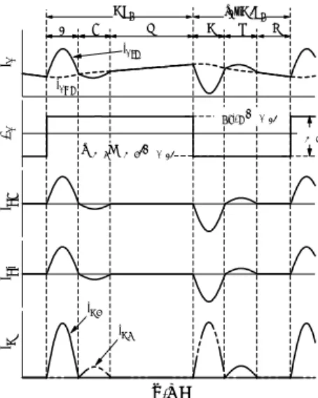
3. Fundamental Operation
The fundamental operation principle of the SCC in the proposed integrated converter is essentially similar to that of conventional SCCs [3], and therefore, this subsection focuses only on the operations of the PWM buck converter and SRVM in the integrated converter. The key operation waveforms in the case that the voltage of B
1, V
1, is the lowest in the energy storage string are illustrated in Fig. 4,
where D is the duty cycle of even-numbered switches in the SCC, and T
Sis the switching period.
The primary winding, including leakage and magnetizing inductances L
kgand L
mg, is driven by a square wave voltage generated at the switching node of Q
5–Q
6. Here, L
mgis assumed to be rather larger than L
kg. In the first three modes, the applied voltage across the primary winding, v
L, is equal to the voltage difference between the PV string and the load (V
String−V
Load), as denoted in Fig. 4, and the current of L
mg, i
Lmg, linearly increases. At the same time, L
kgresonates with C
r, producing sinusoidal current (i
Cr) on the secondary side. Hence, the current of L
kg, i
Lkg, is equivalent to i
Lmgwith the sinusoidal current superimposed on it. In the SRVM, the sinusoidal current preferentially flows through capacitor and diodes that are connected in parallel with the cell having the lowest voltage in the energy storage string [4]. In the discontinuous conduction mode (DCM) operation, no current flows in the SRVM in the third operation mode, and therefore, the third operation mode is identical to the on-period of a traditional PWM buck converter. The next three operation modes are symmetrical to the first three modes; i
Lmglinearly decreases, while sinusoidal current flows in the fourth and fifth modes, similar to the first and second modes.
4. Experimental Results
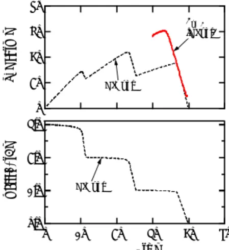
A 100-W prototype of the proposed integrated converter was built, as shown in Fig. 5. The SCC and SRVM including the transformer were separately designed and built in order to measure their individual characteristics, followed by the integration; they were connected using cables. The measured power conversion efficiency of the integrated converter as a while operating at a switching frequency of 200 kHz was approximately 96% at 100 W.
An experimental charge-discharge cycling test using the prototype was performed. Solar array simulators (E4350B, Agilent Technology) were used to emulate a partial shading condition. Before starting the cycling experiment, the duty cycle of the integrated converter was manually varied in order to sweep the PV string characteristic with the equalization by the SCC. The measured PV string characteristics with and without equalization are compared in Fig. 6(a). Multiple power point maxima, including two local and one global MPPs, were found when without the equalization, and
i
Lv
Li
Cri
Cii
DTime
1 2 3 4 5 6
iD2 iD1
DTS (1–D)TS
iLmg iLkg
(VPV1+VPV2)–VLoad
VString–VLoad VPV3
Fig. 4. Key operation waveforms.
Fig. 5. A photograph of a 100-W prototype.
This document is provided by JAXA.
the extractable maximum power was merely 40 W. With the equalization by the SCC, on the other hand, the local MPPs were successfully eliminated, and the extractable maximum power at the load was dramatically boosted to approximately 60 W, proving the efficacy of the PV equalization by the proposed integrated converter.
Four SC modules each with a capacitance of 220 F were used as energy storage modules. The series-connected SC modules were charged with a constant current−constant voltage (CC−CV) charging scheme of 2.0 A−32 V (8.0 V/module), and discharged at 2.0 A using an electronic load.
The resultant charge-discharge cycling profiles are shown in Fig. 6(b).
In the first several cycles, modules of B
3and B
4(V
3and V
4) were overcharged because of their high initial voltages. As the cycling progressed, the voltage imbalance disappeared and the standard deviation of the module voltages gradually decreased because of the voltage equalization by the SRVM. The standard deviation after 8 cycles was approximately 3 mV, demonstrating the equalization performance of the proposed integrated converter.
4. Conclusions
The PWM converter integrating voltage equalizers for PV modules and energy storage cells has been proposed in this paper. The SCC operates as a voltage equalizer for the PV modules while voltages of energy storage cells are equalized by the SRVM. The experimental charge-discharge cycling test was performed emulating a partially-shaded condition for series-connected SC modules from an
initially voltage-imbalanced condition. With the proposed integrated converter, not only was the extractable maximum power from PV modules significantly increased but also voltage imbalance of SC modules was adequately eliminated after several charge-discharge cycles, demonstrating the integrated performance of the proposed integrated converter.
References
[1] T. Shimizu, O, Hashimoto, and G. Kimura, “A novel high-performance utility-interactive photovoltaic inverter system,”
IEEE Trans. Power Electron., Vol. 18, No. 2, pp. 704–711, Mar. 2003.
[2] J. T. Stauth, M. D. Seeman, and K. Kesarwani, “Resonant switched-capacitor converters for sub-module distributed photovoltaic power management,” IEEE Trans. Power Electron., Vol. 28, No. 3, pp. 1189–1198, Mar. 2013.
[3] J. Cao, N. Schofield, and A. Emadi, “Battery balancing methods: a comprehensive review,” in Proc. IEEE Veh. Power and Propulsion Conf., Sep. 2008, pp. 1–6.
[4] M. Uno and A. Kukita, “Bidirectional PWM converter integrating cell voltage equalizer using series-resonant voltage multiplier for series-connected energy storage cells,” IEEE Trans. Power Electron., Vol. 30, No. 6, pp. 3077–3090, Jun. 2015.
3.0 2.0 1.0 0.0
C u rr en t [A ]
50 40 30 20 10 0
V
String[V]
80 60 40 20 0
P o w er [ W ]
PLoad (w/ Eq.)
w/o Eq.
w/o Eq.
(a) Equalization for PV modules.
34 32 30 28 26 24 Total Voltage [V] 22
70 60 50 40 30 20 10 0
Time [min]
9 8 7 6 Module Voltage [V] 5
-4 -2 0 2 4
Current [A]
10-3 10-2 10-1 100
Standard Deviation [V]
VTotal
IES V4
V3
V2 V1