Wakaki HATTORI†a),Nonmember andShigeru YAMASHITA††b),Senior Member
SUMMARY This paper proposes a new approach to optimize the num- ber of necessary SWAP gates when we perform a quantum circuit on a two-dimensional (2D) NNA. Our new idea is to change the order of quan- tum gates (if possible) so that each sub-circuit has only gates performing on adjacent qubits. For each sub-circuit, we utilize a SAT solver to find the best qubit placement such that the sub-circuit has only gates on adjacent qubits. Each sub-circuit may have a different qubit placement such that we do not need SWAP gates for the sub-circuit. Thus, we insert SWAP gates between two sub-circuits to change the qubit placement which is desirable for the following sub-circuit. To reduce the number of such SWAP gates between two sub-circuits, we utilize A* algorithm.
key words: Nearest Neighbor Architecture (NNA), gate order
1. Introduction
After the seminal papers by Shor[1] and Grover[2], there have been intensive researches for quantum computations.
To realize general-purpose quantum computers, one of the major challenges is to find an efficient method to design fault-tolerantquantum circuits[3]in order to overcome the decoherenceproblem. When we perform an operation be- tween distant two qubits, the error due to decoherence would occur frequently. Therefore, it has been considered to per- form quantum circuits on an NNA (Nearest Neighbor Ar- chitecture)[4]where operations only on adjacent qubits are allowed.
To perform arbitrary quantum circuits on an NNA, we need to insert SWAP gates so that the two qubits related to each gate become adjacent. (Note that we assume quan- tum circuits consisting of only two-qubit gates like most of the previous works.) To reduce the number of inserted SWAP gates, there have been many optimization methods proposed; some methods consider the initial qubit place- ment, whereas other methods consider how SWAP gates are inserted.
Indeed there have been researches to develop design methods considering various kinds of NNAs, i.e., for one- dimensional (1D) [4]–[11], two-dimensional (2D) [12]–
[15]and three-dimensional (3D) [16] architectures. As a Manuscript received December 24, 2018.
Manuscript revised June 13, 2019.
Manuscript publicized July 25, 2019.
†The author is with the Graduate School of Information Sci- ence and Engineering, Ritsumeikan University, Kusatsu-shi, 525–
8577 Japan.
††The author is with the College of Information Science and En- gineering, Ritsumeikan University, Kusatsu-shi, 525–8577 Japan.
a) E-mail: [email protected] b) E-mail: [email protected]
DOI: 10.1587/transinf.2018EDP7439
most general model, some researches consider an arbitrary graph where each vertex corresponds to a qubit, and al- low an operation only on the adjacent two vertices in the graph[17]–[19].
Recently, 2D architectures have been studied the most intensively because they have more adjacent qubits com- pared to 1D architectures, and should be much easier to be implemented than 3D ones. For 2D NNAs, PAQCS (Phys- ical Design-Aware Fault-Tolerant Quantum Circuit Synthe- sis)[20]is a good heuristic methodology to reduce the in- serted SWAP gates. To reduce the necessary inserted SWAP gates, PAQCS considers mainly two issues. First, it finds possibly good initial qubit placement based on a graph gen- erated from a each given quantum circuit. Next it finds pos- sibly a good way to “move” (the contents of) qubits in order to make the two qubits related to each gate adjacent.
In the above-mentioned process, PAQCS assumes the gate order is fixed from a given one; it does not consider what is a possibly good gate order to reduce the inserted SWAP gates. Note that almost all previous works for NNAs do not consider the gate order.
Considering the above situation, this paper seeks a new approach to optimize the number of necessary SWAP gates when we map a quantum circuit to a 2D NNA. Our new idea is to change the order of quantum gates (if possible) so that we can decrease the number of sub-circuits which has only gates performing on adjacent qubits. For each sub-circuit, we utilize a SAT solver to find thebestqubit placement such that the sub-circuit has only gates on adjacent qubits in a 2D architecture. This contrasts with PAQCS which find a qubit placement heuristically.
Each sub-circuit may have a different qubit placement such that we do not need SWAP gates for the sub-circuit.
Thus, we insert SWAP gates between two sub-circuits to change the qubit placement which is desirable for the fol- lowing sub-circuit. To reduce the number of such SWAP gates between two sub-circuits, we utilize A* algorithm.
We confirmed that the above-mentioned new approach has a potential to reduce the number of necessary SWAP gates compared with the approach used in PAQCS. Note that we consider a regular 2D architecture in this paper, but our framework can be easily extended to any architecture.
This paper is organized as follows. We review previ- ous design methods for 2D NNAs in Sect. 2. After that, in Sect. 3 we propose our design method, and explain how we can construct a sub-circuit for 2D NNAs, and how we can find a good sequence of inserting SWAP gates in our Copyright c⃝2019 The Institute of Electronics, Information and Communication Engineers
Fig. 1 An example of qubit placement on a 2D grid architecture.
Fig. 2 qubit placement after an operationS(q1,q4) is performed on qubit placement in Fig. 1.
method. We provide some preliminary experimental results in Sect. 4 to show the potential of our idea, i.e., to change the order of gates. Finally, Sect. 5 concludes the paper with our future works.
2. Nearest Neighbor Architectures
In a 2D grid architecture, qubits are placed on a 2D grid as shown in Fig. 1. A qubit has four neighboring qubits at most. For example, in Fig. 1, a qubitq4has four neighboring qubits which areq1,q3,q5andq7.
When an operation is performed on distant qubits such asq0 andq4 in Fig. 1, the decoherence error is more likely to occur. On the other hand, it is expected to reduce the decoherence error by performing a quantum circuit on an NNA. Therefore, to perform a quantum circuit on an NNA, SWAP gates are inserted to swap quantum states, so that a control bit and a target bit are adjacent with each other when we perform an operation on distant qubits. In this paper, S(qi,qj) means a SWAP gate betweenqi andqj. C(qi,qj) means a CNOT gate betweenqiandqj.qiandqjofC(qi,qj) mean a control bit and a target bit ofC(qi,qj) respectively.
When an operation S(q1,q4) is performed on the qubit placement as shown in Fig. 1, the qubit placement is changed to one as shown in Fig. 2. Sinceq0andq4are adja- cent on the qubit placement in Fig. 2,C(q0,q4) is performed on adjacent qubits. Note that we do not change the qubit placementphysicallywhen we perform SWAP gates; only the quantum states of two qubits are swapped when we ap- ply a SWAP gate.
When the initial qubit placement of a quantum circuit in Fig. 3 is one as shown in Fig. 1, for example, we can get circuits as shown in Fig. 4 and Fig. 5 after SWAP gates are inserted. The quantum states of qubits change by inserting SWAP gates, so the output of the quantum circuit will be different from the original one. Thus SWAP gates need to be inserted again to restore the output after all operations.
The number of SWAP gates is 10 in Fig. 4, and the num- ber of SWAP gates is 6 in Fig. 5. As these examples show,
Fig. 3 An example of quantum circuit for explaining insertion of SWAP gates.
Fig. 4 An example of a quantum circuit on an NNA that 10 SWAP gates are inserted into a quantum circuit in Fig. 3.
Fig. 5 An example of a quantum circuit on an NNA that 6 SWAP gates are inserted into a quantum circuit in Fig. 3.
the way of inserting SWAP gates affects the total number of necessary SWAP gates in order to map a quantum circuit to one on an NNA.
3. The Proposed Method
We divide a given quantum circuit into sub-circuits such that all operations in the sub-circuits can be performed without inserting SWAP gates in consideration of changing the gate order. In our proposed method, a SAT solver is used to de- termine if there exists such sub-circuits, and to construct sub-circuits. While constructing sub-circuits, the gate or- der is considered to construct sub-circuits so that they in- clude more gates. After dividing a given quantum circuit into several sub-circuits, SWAP gates are inserted between two sub-circuit to change the qubit placement to the appro- priate qubit placement for each sub-circuit. We employ A*
algorithm to find how to insert SWAP gates to change the qubit placement. A* algorithm is a major searching method
and it is also used to map a quantum circuit to an NNA[17].
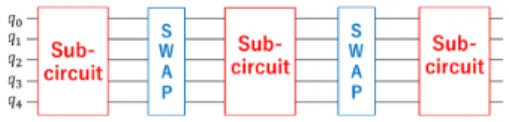
The overall flow of the proposed method is as shown in Algorithm1 and Fig. 6 illustrates an outline of the generated circuits by the proposed method. Details are explained in the following sections.
Algorithm 1Algorithm to divide a given quantum circuit into sub-circuits and to insert SWAP gates between two sub- circuits
1: whilethere exists a quantum gate that is not added to a sub-circuitdo 2: Construct a gate dependency graph of quantum gates that are not
added to sub-circuits
3: Use a SAT solver for a sub-circuit that includes all quantum gates in the gate dependency graph
4: ifUNSATthen
5: Fail⇐the number of quantum gates that are not added to sub- circuits
6: S uccess⇐0
7: whileS uccess−Fail>1do
8: whilethere exists a sub-circuit that contains⌈(S uccess+ Fail)/2⌉quantum gates which is not used for SAT solverdo 9: Use a SAT solver for sub-circuits that contain
⌈(S uccess+Fail)/2⌉quantum gates which is not used for SAT solver
10: ifSATthen
11: S uccess⇐ ⌈(S uccess+Fail)/2⌉
12: break
13: else
14: if we have already checked all the possible sub- circuits having⌈(S uccess+Fail)/2⌉quantum gates by a SAT solver then
15: Fail⇐ ⌈(S uccess+Fail)/2⌉
16: end if
17: end if
18: end while
19: end while 20: end if 21: end while
22: Insert SWAP gates between two sub-circuit by using A* algorithm
3.1 Constructing Sub-Circuits in Consideration of Chang- ing the Gate Order
A gate dependency graph is used to construct sub-circuits of a quantum circuit in consideration of changing the gate order. A gate dependency graph is a directed graph that shows the dependency of quantum gates in a quantum cir- cuit. When quantum gates are not commutative, we define that there is dependency between those quantum gates.
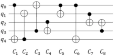
A gate dependency graph of a quantum circuit in Fig. 7 is as shown in Fig. 8. In the quantum circuit in Fig. 7, a tar- get bit ofC1is the same as a control bit ofC2. Thus these quantum gates are not commutative, andC2 must be per- formed after performingC1. In the gate dependency graph
Fig. 7 A quantum circuit that has dependency between quantum gates.
Fig. 8 A gate dependency graph of Fig. 7.
as shown in Fig. 8, there is a directed edge from nodeC1to nodeC2. This means thatC1andC2are not commutative, andC2must be performed after performingC1. There is no path from C2 toC3 (or vice versa) in Fig. 8, and thus we can change the gate order ofC2andC3. While constructing sub-circuits, we consider the gate order by using a gate de- pendency graph to construct sub-circuits that includes more gates.
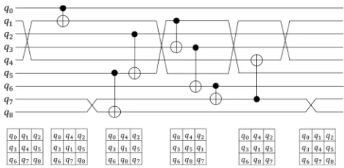
Let us show an example by using a circuit as shown in Fig. 9 and its gate dependency graph as shown in Fig. 10.
In the following, a sub-circuit is denoted by Si, and Si is a set of quantum gates. We first consider S1 = {C1,C2,C3,C4,C5,C6,C7,C8}as a target sub-circuit of the quantum circuit in Fig. 9 that includes the largest number of quantum gates. When a SAT solver is used forS1to find a qubit placement such that all the operations inS1can be per- formed on an NNA architecture, the SAT solver returns that such a qubit placement does not exist. Accordingly, we try a new sub-circuit,S2, which includes half number of quantum gates asS1;S2includes 4 quantum gates.
When constructingS2, it is necessary to select quantum gates from the root of the gate dependency graph in Fig. 10 in order to keep the dependency of quantum gates. Consid- ering the above, we considerS2 ={C1,C2,C3,C4}. When a SAT solver is used forS2 to find a qubit placement that all operations can be performed on an NNA architecture, this time the SAT solver returns that there exists such a qubit placement. Because we want to find a sub-circuit that in- cludes more quantum gates (if there is), we try another new sub-circuit,S3, which contains (|S1|+|S2|)/2=6 quantum gates. This is because we already know that there is a desir- able sub-circuit having|S2|gates, and also there is no such a sub-circuit having|S1|gates, and thus we try to find a circuit having the average number of|S1|and|S2|quantum gates;
this is a standard binary-search technique.
Thus, by considering the dependency of quantum gates, we tryS3 ={C1,C2,C3,C4,C5,C6}afterS2. When a SAT solver is used for S3 to find a qubit placement that all operations can be performed on a NNA architecture, the
Fig. 9 An example of a quantum circuit to explain the constructing method of sub-circuits.
Fig. 10 A gate dependency graph of a quantum circuit in Fig. 9.
SAT solver returns that there does not exist such a qubit placement. Then, for the next trial, we use a SAT solver for S4 ={C1,C2,C3,C4,C6,C8}that also has 6 quantum gates, and then the SAT solver returns that there exists such a qubit placement.
Accordingly, in the same way as constructing S3, we construct another new sub-circuit, S5, which includes (|S1| +|S4|)/2 = 7 quantum gates. Thus, by consider- ing the dependency of quantum gates, we consider S5 = {C1,C2,C3,C4,C5,C6,C8}next. When a SAT solver is used forS5, the SAT solver returns that there does not exist such a qubit placement. When a SAT solver is used for another sub-circuit that also has 7 quantum gates, the SAT solver returns that there does not exist such a qubit placement.
In conclusion,S4in Fig. 11 is a sub-circuit that has the largest number of quantum gates for our purpose. We can find a sub-circuit including the largest number of quantum gates by the above-mentioned binary search-based method.
Usually a sub-circuit containing the largest number of gates seems to be a good choice. However, sometimes such a sub-circuit needs too many SWAP gates to get the qubit placement for the sub-circuit. If we select such a sub-circuit, the final result may become worse. So, we try to select pos- sibly the best sub-circuits as follows. We check how many SWAP gates are needed to get the qubit placement for all the possible sub-circuits to be performed on an NNA architec- ture. Then we select one sub-circuit such that the number of gates in the sub-circuit divided by that of inserted SWAP gates is the largest.
3.2 Qubit Placement with a SAT Solver
In the following, we consider qubits are placed on a 2D grid as shown in Fig. 13. If we choose the qubit placement as shown in Fig. 13, the control and the target bits are adja- cent for all CNOT gates in the quantum circuit as shown in Fig. 12. Thus all operations in Fig. 12 can be performed
Fig. 11 sub-circuitS4={C1,C2,C3,C4,C6,C8}.
Fig. 12 A quantum circuit in which all operations can be performed on NNA without inserting SWAP gates.
Fig. 13 A qubit placement that allows the quantum circuit in Fig. 12 to be performed on an NNA without inserting any SWAP gate.
without inserting SWAP gates on this qubit placement.
In the following, we propose a method to find such a good 2D placement based on a Boolean satisfiability prob- lem (SAT). Namely, we formulate a qubit placement prob- lem as a Boolean function (i.e., a SAT problem instance) as follows: the derived Boolean function is satisfiableif and only if there exists a qubit placement for a given quantum circuit to be performed on an NNA without inserting SWAP gates. A SAT solver as explained below is used to figure out that such a qubit placement exists, and if it exists, the solver also finds how qubits are placed.
A SAT solver determines the satisfiability of a given Boolean function, and it can also provide a satisfying as- signment when the problem is satisfiable. In our proposed method, one variable is used to express whether or not each qubit is placed on each cell on a 2D grid, and all the nec- essary conditions are expressed by Boolean formulas with such variables as we will explain in the following.
The following three conditions are needed to assign qubits on a 2D grid such that all operations in a sub-circuit can be performed without inserting SWAP gates.
Condition 1 A control bit and a target bit of all gates are adjacent.
Condition 2 Each qubit is assigned to only one cell on a 2D grid.
Condition 3 At most one qubit is assigned to each cell on a 2D grid.
As shown in Fig. 14, a cell of rowiand column jon a 2D grid is expressed as (i,j). Logical variablexi,j,kexpresses
whether qubitqkis assigned to (i,j) or not. Namely, when qubitqkis assigned to (i,j),xi,j,kbecomes 1. Otherwisexi,j,k becomes 0. For example, ifq1 is assigned to (2,0), x2,0,1
becomes 1. Ifq1is not assigned to (2,0),x2,0,1becomes 0.
First we consider the expression for Condition 1. For example, when there is a CNOT gate that hasq2as a control bit andq4as a target bit,q2andq4have to be assigned adja- cently. Thus, ifq2is assigned to (1,1),q4has to be assigned to either one of (0,1), (1,0), (1,2) or (2,1). Accordingly, whenx1,1,2is 1, either ofx0,1,4,x1,0,4,x1,2,4orx2,1,4has to be 1. This condition can be expressed as Eq. (1).
(¬x1,1,2)∨(x0,1,4∨x1,0,4∨x1,2,4∨x2,1,4) (1) We consider such conditions of assigning q2 and q4
to adjacent qubits for each cell. Then, by ORing all the Boolean formulas for such conditions, we get a formula for the condition such thatq2 andq4should be placed ad- jacently. We consider such formulas for each pair of control and target bits for all gates, and we get the formula for Con- dition 1 by ANDing them.
Next we consider the expression for Condition 2. For example,q0has to be assigned to only one of cells on a 2D grid. This can be realized by considering the following two conditions: The first one is thatq0is assigned to at least one cell, and the second one is thatq0is assigned to at most one cell on a 2D grid.
The former condition can be expressed as at least one of xi,j,0 has to be 1. Thus, as shown in Eq. (2), sum of xi,j,0 needs to be 1. The condition also can be expressed as Eq. (3).
∑
i,j
xi,j,0=1 (2)
x0,0,0∨x0,1,0∨x0,2,0∨ · · · ∨xi,j,0 (3) The latter condition can be expressed as follows: For exam- ple, if we do not wantx0,0,0 andx0,1,0 to be 1 at the same time, we have Eq. (4) which means x0,0,0 and x0,1,0 cannot be 1 at the same time. That is, when Eq. (4) holds,q0cannot be assigned to both of (0,0) and (0,1) at the same time.
¬x0,0,0+¬x0,1,0=1 (4)
We consider similar formulas for all pairs of cells on a 2D grid as shown in Eq. (5). By ANDing these formulas, we have formulas for Condition 2 only forq0.
¬xi,j,0+¬xk,l,0 =1 ((i,j),(k,l)) (5) If Eq. (3) and Eq. (5) hold,q0is assigned to at least one of
At this time, no more than one qubit needs to be assigned to each cell. For example, Eq. (6) expresses a condition that prohibits assigningq0andq1to (0,0) at the same time.
¬x0,0,0+¬x0,0,1 =1 (6)
We consider similar formulas for all pairs of qi andqj as shown in Eq. (7). By ANDing these formulas, we get a for- mulas of the condition that only one qubit is assigned to (0,0). We consider similar formulas for each cell, and we get the expression for Condtion 3 by ANDing them.
¬x0,0,i+¬x0,0,j=1 (i, j) (7) By ANDing the above expressions for Conditions 1, 2 and 3 all together, we finally obtain a SAT formula for our purpose. Thus, by using a SAT solver, we can determine if there exists a good qubit placement that allow us to perform a given circuit on an NNA without inserting SWAP gates. If such a qubit placement exists, a SAT solver find an satisfy- ing variable assignment as well.
There may be a case when several qubit placements can satisfy the conditions. To get another satisfying variable assignment, we use a SAT solver repeatedly with adding the negated conditions obtained before. In such a case, we adopt a qubit placement with the smallest values of h∗(n) which is a cost function to measure the quality of an intermediate solution in A* algorithm, which will be explained in detail in the next section.
3.3 Inserting SWAP Gates by A* Algorithm
After dividing a given quantum circuit into sub-circuits each of which can be performed without inserting SWAP gates, our remaining task is to insert SWAP gates between each pair of two sub-circuits to change the qubit placement so that each sub-circuit can be performed without inserting SWAP gates. We utilize A* algorithm to decide the way of inserting SWAP gates as we will explain in the following.
A* algorithm searches a graph to find a way from the start node S to the goal nodeG based on a cost function f∗(n) which is the sum ofg∗(n) andh∗(n) as shown in Eq. (8) wherenmeans a node found during the search of a way in the graph. g∗(n) is a cumulative cost from the start node to the current node,n, andh∗(n) is a heuristic function that estimates the cost from the current node,n, to the goal node.
f∗(n)=g∗(n)+h∗(n) (8) Algorithm 3 shows our A* algorithm which inserts SWAP gates to change the qubit placement. We add a searched node to theopen list. We sort the nodes in the open list based on f∗(n). A node with the least f∗(n) in the open
list is popped from the open list, and added to the closed list. This means that we select the node with the least f∗(n) as promising to search first, and so we add all the nodes connected to it (i.e., the nodes we can reach by one move from the selected node) into the open list. These processes are repeated until we get to the goal, i.e., the objective qubit placement.
Each node in a graph used for our A* algorithm corre- sponds to a qubit placement. If two nodes are connected in the graph, a single SWAP gate can change the qubit place- ments between the two placements corresponding to the two nodes. In the following,S is the qubit placement of one sub- circuit andGis the one of the following (next) sub-circuit;
we find a way of inserting SWAP gates between two sub- circuits by searching a shortest path fromS toGin the graph for the A* algorithm.
g∗(n) is the number of moves to reachnfromS. That is, the number of necessary inserted SWAP gates to get to the qubit placement corresponding ton.h∗(n) is the sum of manhattan distance between the locations of qubitqiin the qubit placement corresponding tonand the objective qubit placement. When the qubit placement corresponding ton andGare as shown in Fig. 15 and Fig. 16, respectively,h∗(n) is calculated as follows.q0is located on (1,1) inn. On the other hand, it is located on (0,0) inG. Thus, the manhattan distance ofq0in these qubit placements is 2. The manhattan distance for other qubits is calculated in the same way, and the sum of the manhattan distance is as shown in Eq. (9).
Algorithm 3A* algorithm inserting SWAP gates to change the qubit placement
1: Initialize the open list and the closed list 2: Add the starting node to the open list 3: whilethe open list is not emptydo 4: m←openlist.pop()
5: Addmto the closed list
6: for eachm´ such that ´mis a qubit placement obtained frommby inserting a single SWAP gatedo
7: ifthe qubit placement ´mis equivalent to the one corresponding toGthen
8: break
9: end if
10: Calculatef∗( ´m) and add ´mto the open list 11: end for
12: Sort nodes in the open list based onf∗() 13: end while
h∗(n)=2+1+2+1=6 (9) We show an example of inserting SWAP gates by A*
algorithm as follows. In the example, we consider insert- ing SWAP gates to change the qubit placement from the one corresponding toS as shown in Fig. 15 to the one corre- sponding toGas shown in Fig. 16.
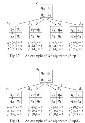
OL andCLstand for the open list and the closed list, respectively. At first, OL is {S} and CL is {} since S is the start node. Therefore,S is popped fromOLand added
Fig. 15 An example of qubit placement.
Fig. 16 The qubit placement corresponding toGafter inserting SWAP gates.
Fig. 17 An example of A* algorithm (Step1).
Fig. 18 An example of A* algorithm (Step2).
to CL. As shown in Fig. 17, there are four ways to in- sert a SWAP gate to the qubit placement S and they are S(q2,q3),S(q1,q3),S(q0,q1) andS(q0,q2). These nodes are added toOLand then,OLis{A1(5),A3(5),A4(5),A2(9)}af- ter it is sorted based on f∗(n) which are in the parenthesis.
A1 is popped from OL and added to CL because A1 is one of the nodes whose f∗(n) is the small- est. Therefore, CL becomes as {S,A1(5)}. There are four ways to insert a SWAP gate to the qubit placement A1 and they are S(q2,q3),S(q1,q2),S(q0,q1) and S(q0,q3) as shown in Fig. 18. Since OL be- comes as{B3(4),A3(5),A4(5),B2(6),B4(6),B1(8),A2(9)},B3
is popped fromOLand added toCL. Then,CLbecomes as {S,A1(5),B3(4)}.
Similarly, there are four ways to insert a SWAP gate in the qubit placementB3as shown in Fig. 19 and they are S(q2,q3),S(q0,q2),S(q0,q1) andS(q0,q3). NowC2 is the same qubit placement as the one corresponding toG, and so A* algorithm finishes.
The above example shows that it is possible to
Fig. 19 An example of A* algorithm (Step3).
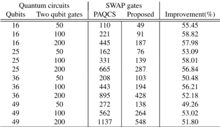
Table 1 The comparison between PAQCS and our proposed method.
Quantum circuits SWAP gates
Qubits Two qubit gates PAQCS Proposed Improvement(%)
16 50 110 49 55.45
16 100 221 91 58.82
16 200 445 187 57.98
25 50 162 76 53.09
25 100 331 139 58.01
25 200 665 287 56.84
36 50 208 103 50.48
36 100 443 194 56.21
36 200 895 428 52.18
49 50 272 138 49.26
49 100 562 264 53.02
49 200 1137 548 51.80
change the qubit placements corresponding to the change from S to G by inserting SWAP gates in the order of S(q2,q3),S(q0,q1),S(q0,q2). Thus, by using the above A*
algorithm, it is able to find a way of inserting SWAP gates to change the qubit placement for the following sub-circuit.
4. Experimental Results
We implemented the proposed method and PAQCS[20]in C++to evaluate the performance of the proposed method.
We generated 300 random benchmark quantum circuits con- sisting of only two-qubit gates whose control and target bits are chosen randomly. Then, we applied the proposed method and PAQCS to them in order to compare the aver- age number of inserted SWAP gates. In the experiment, we utilized GlueMiniSat 2.2.8 for a SAT solver and a 4.20 GHz i7-7700K CPU with 16 GB RAM.
Each row of Table 1 reports the average number of inserted SWAP gates of 300 different random circuits by our method and PAQCS. Our proposed method can reduce the number of inserted SWAP gates by 54.43% on average compared to PAQCS. Even for larger quantum circuits, our method can find the solution within 10 minutes; On the other hand, PAQCS takes less than a minute. We confirmed that changing the order of quantum gates makes it possible to perform more gates on the same qubit placement (without inserting SWAP gates). We consider that this would be one reason why our method can reduce the inserted SWAP gates.
Our method inserts SWAP gates between each sub- circuit, and thus the number of sub-circuits affects the num-
PAQCS may need to insert SWAP gates even in the same case because PAQCS determines the initial qubit placement heuristically unlike our method.
Note that both the SAT solver and the A* search used in our method need exponential time to the problem size.
However, our experimental results show that our method can treat quantum circuits that are available currently like IBM- Q or in the near future. If much larger quantum circuits are available in the future, we may need to divide a large circuit into sub-circuits so that our method can treat each sub-circuit.
5. Conclusion
In this paper, we proposed a new idea to map a quantum circuit so that we can perform on an NNA; we proposed to change the order of quantum gates to decrease the number of inserted SWAP gates. By means of changing the order of quantum gates, we can indeed decrease the number of sub- circuits in which all the gates perform on adjacent qubits.
We utilize a SAT solver to find a good qubit placement such that the sub-circuit has only quantum gates performing on adjacent qubits in 2D architecture. Moreover, we utilize A* algorithm to insert SWAP gates for changing the qubit placement between two sub-circuits. As a result, we can reduce the number of inserted SWAP gates compared to the state-of-the-art heuristic, PAQCS.
In our proposed method, the performance of A* algo- rithm get worse when the target quantum circuit become larger. Thus, our future work is to find a way to insert SWAP gates to change the qubit placement more efficiently than our current A* algorithm. Also, as our future work, we should evaluate our framework by using benchmark circuits which are used in the research community of quantum circuit de- sign.
Acknowledgments
This work was supported by JSPS KAKENHI Grant Num- ber 15H01677 and 18K19790, and by the Asahi Glass Foun- dation.
References
[1] P.W. Shor, “Polynomial-time algorithms for prime factorization and discrete log- arithms on a quantum computer,” SIAM J. Comput., vol.26, no.5, pp.1484–1509, 1997.
[2] L.K. Grover, “A fast quantum mechanical algorithm for database search,” Proc. Twenty-Eighth Annual ACM Symposium on Theory of Computing, pp.212–219, 1996.
[3] H. Goudarzi, M.J. Dousti, A. Shafaei, and M. Pedram, “Design of a universal logic block for fault-tolerant realization of any logic op- eration in trapped-ion quantum circuits,” Quantum Information Pro- cessing, vol.13, no.5, pp.1267–1299, May 2014.
[4] Y. Hirata, M. Nakanishi, S. Yamashita, and Y. Nakashima, “An Effi- cient Conversion of Quantum Circuits to a Linear Nearest Neighbor Architecture,” Quantum Info. Comput., vol.11, no.1, pp.142–166, Jan. 2011.
[5] R. Wille, M. Saeedi, and R. Drechsler, “Synthesis of Reversible Functions Beyond Gate Count and Quantum Cost,” arXiv preprint arXiv:1004.4609, 2010.
[6] R. Wille, A. Lye, and R. Drechsler, “Optimal SWAP gate insertion for nearest neighbor quantum circuits,” 2014 19th Asia and South Pacific Design Automation Conference (ASP-DAC), pp.489–494, IEEE, 2014.
[7] M. Saeedi, R. Wille, and R. Drechsler, “Synthesis of quantum cir- cuits for linear nearest neighbor architectures,” Quantum Informa- tion Processing, vol.10, no.3, pp.355–377, June 2011.
[8] A. Shafaei, M. Saeedi, and M. Pedram, “Optimization of quantum circuits for interaction distance in linear nearest neighbor architec- tures,” Proc. 50th Annual Design Automation Conference, Article No. 41, ACM, 2013.
[9] M.M. Rahman and G.W. Dueck, “Synthesis of linear nearest neigh- bor quantum circuits,” arXiv preprint arXiv:1508.05430, 2015.
[10] A. Chakrabarti, S. Sur-Kolay, and A. Chaudhury, “Linear near- est neighbor synthesis of reversible circuits by graph partitioning,”
arXiv preprint arXiv:1112.0564, 2011.
[11] A. Matsuo and S. Yamashita, “Changing the gate order for optimal LNN conversion,” International Workshop on Reversible Computa- tion, LNCS, vol.7165, pp.89–101, Springer, 2011.
[12] A. Shafaei, M. Saeedi, and M. Pedram, “Qubit placement to min- imize communication overhead in 2D quantum architectures,”2014 19th Asia and South Pacific Design Automation Conference (ASP- DAC), pp.495–500, IEEE, 2014.
[13] D. Ruffinelli and B. Bar´an, “Linear nearest neighbor optimization in quantum circuits: a multiobjective perspective,” Quantum Informa- tion Processing, vol.16, no.9, p.220, 2017.
[14] R. Wille, O. Keszocze, M. Walter, P. Rohrs, A. Chattopadhyay, and R. Drechsler, “Look-ahead schemes for nearest neighbor optimiza- tion of 1D and 2D quantum circuits,” 2016 21st Asia and South Pacific Design Automation Conference (ASP-DAC), pp.292–297, IEEE, 2016.
[15] A. Farghadan and N. Mohammadzadeh, “Quantum circuit physical design flow for 2D nearest-neighbor architectures,” Int. J. Circuit Theory and Applications, vol.45, no.7, pp.989–1000, July 2017.
[16] C.A. P´erez-Delgado, M. Mosca, P. Cappellaro, and D.G. Cory, “Sin- gle spin measurement using cellular automata techniques,” Phys.
Rev. Lett, vol.97, no.10, p.100501, 2006.
[17] A. Zulehner, A. Paler, and R. Wille, “An Efficient Mapping of Quantum Circuits to the IBM QX Architectures,” arXiv preprint arXiv:1712.04722, 2017.
[18] A. Lye, R. Wille, and R. Drechsler, “Determining the minimal num- ber of swap gates for multi-dimensional nearest neighbor quantum circuits,” 2015 20th Asia and South Pacific Design Automation Con- ference (ASP-DAC), pp.178–183, IEEE, 2015.
[19] D. Bhattacharjee and A. Chattopadhyay, “Depth-Optimal Quan- tum Circuit Placement for Arbitrary Topologies,” arXiv preprint arXiv:1703.08540, 2017.
[20] C.C. Lin, S. Sur-Kolay, and N.K. Jha, “PAQCS: Physical Design- Aware Fault-Tolerant Quantum Circuit Synthesis,” IEEE Trans. Very Large Scale Integration (VLSI) Systems, vol.23, no.7, pp.1221–
1234, July 2015.
Wakaki Hattori received the B.E. degrees in Information Science and Engineering from Ritsumeikan University in 2018. He is currently a graduate student of Graduate School of Infor- mation Science and Engineering, Ritsumeikan University, Shiga, Japan. His research interests include quantum circuit design, quantum cost reduction and synthesis of Nearest Neighbor Ar- chitecture.
Shigeru Yamashita is a professor at the Department of Computer Science, Col- lege of Information Science and Engineering, Ritsumeikan University. He received his B.E., M.E. and Ph.D. degrees in Information Science from Kyoto University, Kyoto, Japan, in 1993, 1995 and 2001, respectively. His research in- terests include new types of computation and logic synthesis for them. He received the 2000 IEEE Circuits and Systems Society Transactions on Computer-Aided Design of Integrated Cir- cuits and Systems Best Paper Award, SASIMI 2010 Best Paper Award, 2010 IPSJ Yamashita SIG Research Award, and 2010 Marubun Academic Achievement Award of the Marubun Research Promotion Foundation. He is a senior member of IEEE, and a member of IPSJ.