効率的なFPGA実装を指向したニューラルネットワークのアーキテクチャ
6
0
0
全文
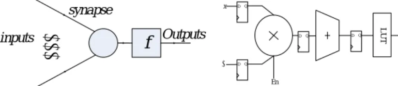
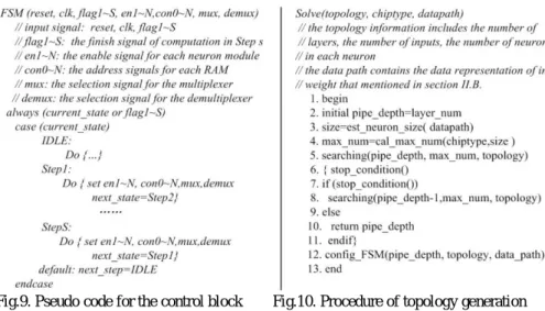
(2) Vol.2010-SLDM-145 No.11 2010/5/20. 情報処理学会研究報告 IPSJ SIG Technical Report. be mapped together at a time, according to the adopted FPGA chip and neural network topology. The upper limit of neurons count implemented in a single chip should be taken into consideration, and when the total number of neurons in the neural network to be implemented is smaller than this value, the physical neural architecture in FPGA chip maybe organized as whole pipeline manner to get the highest implementation speed, and on the other hand, the working manner specified as partly pipeline based on layer multiplexing that try to get the optimal tradeoff between the speed and cost. The rest of this paper is organized as follows: Section II describes the circuit design of the single neuron and Section III presents the detail of the proposed architecture. Section IV validates the advantages of proposed method by the experiment. Finally, Section V concludes the paper.. Figure 2 show the block diagram of the neuron circuit, where En is an enable signal that controls the neuron’s state, working or not. The selection of word length/bit precision has an important impact on the output resolution, where longer bits means higher resolution but also larger resource cost. And in actually ANNs design, these parameters are set according to the application in order to achieve the efficient hardware implementation. In this paper, we perform the parameters as a variable, which can be modified by users in compilation time. Assume that the input x normalized in the range of 0 to 1 and is Ni bits, 1 bit for sign and (N i-1) bits for data. The weights are also represented in Nw bits: 1 bit for sign, Nww bits for integer part and Nwf bits for fraction part, where Nw= Nww + Nwf +1. After multiplied and accumulated, the result becomes to Nr bits length: 1 bit for sign, Nww + Nrw bits for integer part and Nwf bits for fraction part, where Nr= Nww + Nrw + Nwf +1. The result of the active function is obtained as a signed Ni bits number, which is the same as the input. The active function is realized by using LUT(look up table)[7] according to the fact that the modern FPGA chip has large number of built-in RAMs. As the active function is highly nonlinear, a general procedure to obtain an LUT of minimum size for a given resolution is as follows. 1) As mentioned before, the bit length of output from active function (formula 2) is Ni. 2) The actual output of active function is between 2-Ni and 1- 2-Ni when using the bit length Ni. Let x1 and x2 be the upper and lower limits of the input range, that is:. 2. NEURON DESIGN Mathematical Model A multilayer neural network is composed of one input layer which stores the input data, several hidden layers for computation and one output layer. Each layer consists of a set of processing elements called neuron and the main task of each neuron in neural networks is processing the following function: 𝑦 = 𝑓 𝑥 = 𝑓( 𝑛𝑖=1 𝜔𝑖 𝑥𝑖 + 𝑏) (1) where xi stand for the ith input, and 𝜔𝑖 is the weight in the ith connection and b is the bias. The function f(x) is the nonlinear active function used in the neuron. Here we select the log-sigmoid as the active function due to its popularity, and it is described by the following: 2.1. 1. 𝑓 𝑥 = 1+𝑒 −𝑥. 1 1+𝑒 −𝑥 1. x. (2). ∑. f. (𝐿𝑈𝑇)𝑚𝑖𝑛 = D. D. Q. D. Q. 𝑥 1 −𝑥 2 ∆𝑥. (6). 3. Network Design. Q. The function of network is to connect all the neurons and all the layers together, so the data can be forward through the connections from former layer to the latter layer. Fig.4 gives an example of multilayer neural network.. En. Fig.1. mathematical model of a neuron. (5). 4) The minimal number of LUT values is given by. Q. Outputs ω. 0.5+2−𝑁𝑖. ∆𝑥 = ln (0.5−2−𝑁𝑖 ). LUT. .... inputs. D. (3). By solving (3) as x is variable, we can get: 𝑥1 = − ln 2𝑁𝑖 − 1 , 𝑥2 = +𝑙𝑛 2𝑁𝑖 − 1 (4) -Ni 3) Consider the fact that the step change in the output (△y) is equal to 2 , and the corresponding minimum change in input is at the point of maximum slope, x = 0 in this case. So the minimal change value of input for the output change of 2-Ni can be obtained from. Because the weights are stored in RAM that can be easily modified, we did not develop the online learning in our proposed architecture. 2.2 Neuron Circuit Design As mentioned above, the computational resources required by a single neuron are multiplication block, accumulation block and active function block.. synapse. 1. = 2−𝑁𝑖 , 1+𝑒 −𝑥 2 = 1 − 2−𝑁𝑖. Fig.2. Neuron circuit block diagram 2. ⓒ2010 Information Processing Society of Japan.
(3) Vol.2010-SLDM-145 No.11 2010/5/20. 情報処理学会研究報告 IPSJ SIG Technical Report. . . . .. NK. computing for the input pattern m and neurons in the next layer are idle because they are waiting for the input coming from neurons in the previous layer. Secondly, when the neural computing has been completed, they send their result as input for the neuron in the next layer. So the neurons in the second layer become to work and the neurons in first layer are waiting for the end of this forwarding for input pattern m. At the last, when the signal arriving at the output layer, the other two would be in the idle or waiting state. Only the neurons in the output layer have accomplished they calculation and get the final result, the forwarding for the input pattern m could be over and there would be the next forwarding for another input pattern.. . . . .. NK-1 . . . .. . . . .. N1. . . . .. N0 waiting. Disabled input. working. Fig.3. The experimental result between original and LUT. Fig.4. Multilayer neural network. Disabled neuron. Assume the symbols 𝑥𝑘𝑖𝑗 and 𝑦𝑘𝑖 , stand for the input and output of neurons,. a. b. respectively, where k is the layer number, i is the neuron number in this layer and j is the jth input of this neuron. Suppose the ID for input layer is 0, then the forward process can be described as follows.. t t-1 t-2. 𝑁0. 𝑤𝑗𝑖01 ∙ 𝑥𝑗 , 𝑖 ∈ 1, 𝑁1 , 𝑗 ∈ 1, 𝑁0. 𝑦1𝑖 =. c. 𝑗 =1 𝑖𝑗. 𝑗. 𝑥𝑘 = 𝑦𝑘−1 , 𝑦𝑘𝑖 =. 𝑁𝑘 −1 𝑗 =1. (𝑘−1)𝑘. 𝑤𝑗𝑖. ∙ 𝑥𝑖𝑗. Fig.5. Non-pipeline vs pipeline. (7). (𝑘−1)𝑘. Fig.6. The process of layer multiplexing. In the conventional non-pipeline forward phase, there is only one layer working busily while the other layers just waiting. In order to save the cost, we integrate the pipeline manner in the layer architecture when forwarding. The fundamental pipeline algorithm is described as follows, where the symbol t is the time factor given by clock cycle.. k ∈ 2, NK , i ∈ 1, Nk , j ∈ 1, Nk−1 Where Nk is the total number of neurons in layer k, and 𝑤𝑗𝑖. Step1 Step2 Step3. d. stands for the weight. between the jth neuron in layer (k-1) and the ith neuron in the layer k. Especially, the symbol Nk in Fig.4 means the total number of layers in this network and N0 is the input number. There are two concept of our proposed network architecture, including pipeline design and layer multiplexing design. 3.1 Pipeline Design As mentioned above, the multilayer neural network has a characteristic that the neuron in the next layer depends on the neuron in the previous layer and there is no communication among neurons in the same layer. As shown in figure 5 (a, b, c), for an input pattern m, the traditional forward phase work as: firstly, the neuron in the first layer performs the neural. N0. y1i (t ) w01 ji x j (t ), i [1, N1 ], j [1, N 0 ]; j 1. N k 1. N k 1. N0. j 1. j 1. j 1. N k 1. N k 1. N k 1. N0. j 1. j 1. j 1. j 1. y 2i (t ) w12 ji y1j (t 1) w12 ji w01 ji x j (t 1). (8). y3i (t ) w 23 ji y 2j (t 1) w 23 ji w12 ji w01 ji x j (t 2). 3. ⓒ2010 Information Processing Society of Japan.
(4) Vol.2010-SLDM-145 No.11 2010/5/20. 情報処理学会研究報告 IPSJ SIG Technical Report. As shown in figure 5 (d) and formula (8), when the first layer is under computing for the input pattern t, the second layer is busy calculating the result for pattern t-1 which is transmitted by the first layer in the last cycle. It doesn’t need to wait for the end of some input pattern forwarding, but all the neurons in different layers are working simultaneously with different input pattern. By using the pipeline, the global forwarding speed would be much higher than the non-pipeline method. And comparing with non-pipeline method, there would not be much incidental cost or changes in the architecture by using proposed pipeline method, but just some modifications based on the old one, such as: 1) Enhance the clock rate for input memory module according to the pipeline depth. 2) Allocate a dependant memory for each neuron to store the weights. 3) Add a register to store the output of each neuron. Unfortunately, due to the limited resource on FPGA, it is impossible to perform a whole neural network as pipeline manner in a single FPGA chip whose price is reasonable for commercial or industrial application. To solve this problem, we introduce the layer multiplexing into our pipeline method. 3.2 Layer Multiplexing with Partly Pipeline Layer multiplexing was first proposed by S.Himavathi in 2007 [6], which aimed at reducing the resource requirement by multilayer neural network. Instead of realizing a complete network, only the single largest layer with each neuron having maximum number of input is implemented. The same layer behaves as different layers with the help of a control block. For example, consider a 3-5-4-2 network. The largest layer has five neurons and the maximum number of input is five, so in actually execution, there are only five neuron modules with each neuron having five inputs. A simple process of layer multiplexing for the given network is shown in figure 6. For the execution of the first layer, the whole five neurons would be enabled with disabling the other input synapses because the neuron in the first layer only need three input synapses. The working of the second and the third layer is almost the same as the first layer, identified as Step2 and Step3 in figure 6, respectively. The control block ensures proper functioning by assigning the enable signal, appropriate inputs and weights for each neuron. This method presents an advantage that it can largely save the resource so that a larger network could be performed in a single FPGA chip so far as the largest single layer can be realized on this chip. But this success is achieved at the expense of losing the global forwarding speed, because there is only one layer being working and it has to reconfigure the network before performing neural computing in the next layer. When the network has more layers this problem becomes worse which may cause the timing violation in some. speed-sensitive application. From the synthesis report of [6], when implementing an 8-5-5-3 network by layer multiplexing, the utilization rate of slice is only 62%, that is, we still have enough slice resource to do some improvement to make the global forwarding speed higher. The main idea in this paper is adding the partly pipeline manner to the layer multiplexing method. In our proposed method, we first calculate the maximum number of neuron modules to fit an adopted FPGA chip. And then taking this value and the neural network topology into consideration, we can get an optimal solution by assigning the appropriate mapping method, pipeline depth and layer multiplexing. Figure 7 gives an example of our method.. Fig.7. The schematic of our Fig.8. The network circuit mapping method In this example, we suppose the network topology intends to be realized is 3-4-2-3-1, the maximum number of neuron modules the FPGA supported by is six. Numbers in the nodes in figure 7 mean the layer numbers. It performs the neural computing of two layers at a time with the pipeline manner between these two layers. In Step1, the first two layers are under 4. ⓒ2010 Information Processing Society of Japan.
(5) Vol.2010-SLDM-145 No.11 2010/5/20. 情報処理学会研究報告 IPSJ SIG Technical Report. working, where the layer 1 is computing for the input pattern am+1 and the layer 2 is serving for input pattern am, respectively. And in Step2, the 2nd and 3rd layers are configured by the layer multiplexing mechanism, where the 2 nd layer is busy with input pattern am+1 from the layer 1 in the previous step while the 3 rd layer is computing for input pattern am from layer 2 by layer multiplexing. And the total number of neurons in the 2nd and 3 rd layers is five, so there are disabled neuron modules to save the power. The next steps are almost the same as the first two steps, including enable the proper number of neuron modules, get the corresponding input from previous step, perform neural computing for the incoming data and then send the result to the next step by layer multiplexing. And if the computation in Step4 is completed, it would turn to the Step1, forming a loop. In this example, there are always two layers mapping the neuron modules in pipeline, which means the pipeline depth is two. By assigning different FPGA chip and neural network topology, the pipeline depth may be different. 3.3 The Network Circuit Design The operation of layer multiplexing and the partly pipeline is guaranteed by a control block, which is realized by the finite state machine (FSM). Figure 8 shows the whole circuit of neural network using our proposed method. The details of the block named NEURON is already presented in section II, so we will introduce the control block design here.. Fig.9. Pseudo code for the control block. RAMs, the multiplexer and demultiplexer, and performing the logical data transmission. The pseudo code of the FSM is given in figure 9.We also developed a MATLAB program to determine the optimal architecture for a given neural network and a selected FPGA chip. Firstly, it estimates the number of slices would be utilized by a neuron module when the data structure of the neuron is given. Secondly, the maximum amount of neuron modules allowed in the selected FPGA chip can be figured out due to we have integrated the information of several popular FPGA chip into the procedure. Then a searching function will be invoked to determine the optimal pipeline depth for the neural network. This procedure also provides the function that configures the parameters in the FSM. The pseudo code of the procedure is shown in figure 10.. 4. Experiments FPGA design flow is as follows: 1) design entry, 2) synthesis, 3) simulation and 4) devices programming. We choose the Verilog HDL as the coding language for design entry and Xilinx ISE 9.1i to do the synthesis and devices programming while the simulation is performed by Modelsim XE II 7.3a. The FPGA chip we selected here is Virtex XCV400hq240, which is widely used in commercial or industrial application as their lower price. The basic block of the Virtex is the Logic Cell (LC)[8], which is composed of a four inputs LUT, carry logic and a Flip-Flop. And two LCs form the slice, which is used to measure the resource cost. Table I gives the synthesis report for a single neuron module by varying the data path in weights, because in most cases the input is always fixed at 9 bits with different weight bit lengths. From the table we can see that with respect to the increase of data precision, the maximum frequency comes down but at an acceptable level. Table II is the synthesis report for the example neural network mentioned in Section III B. The value of pipe depth means the number of layers under execution at a time. From the table we can obtain that our proposed architecture is compact due to the simple module architecture and the effective control block, and also provides a flexible solution for a neural network to be implemented because the pipeline depth is adaptive to the selected FPGA chip and the network topology. Table III shows a comparison between the traditional layer multiplexing method (LM) and our proposed method. We have integrated the partly pipeline manner into the layer multiplexing, there are several layers mapping the neuron modules by pipeline manner while LM only maps one layer at a time. As a result, the global forward speed of our method is much higher than LM with respect to the pipeline depth. The CPS (connection per second) is used to evaluate the throughput of neural network. Due to the pipeline manner, our method has much more neurons under working than the conventional LM, so it also shows an. Fig.10. Procedure of topology generation. The main task of the control block is assigning proper signals for the input and weight 5. ⓒ2010 Information Processing Society of Japan.
(6) Vol.2010-SLDM-145 No.11 2010/5/20. 情報処理学会研究報告 IPSJ SIG Technical Report. advantage in CPS when compared with LM.. parameter values to match the particular network size and running the synthesis. Similarly to a particular network, the best solution of the architecture design of pipeline and layer multiplexing is calculated by a MATLAB procedure, by returning the optimal pipeline depth and the control signal value in each state of the control block (FSM). We exploited the capability of a given FPGA chip by assigning the proper pipeline depth, so that a higher resource utilization rate and global forward speed were achieved. It is easy to design a FPGA implementation for a given neural network at a short time by varying the data path. It also provides the feasibility to perform a larger neural network in a lower-performance FPGA chip at a relatively higher speed by using the partly pipeline method. So it is possible to develop a neural device for commercial or industrial application by our method.. T ABLE I RESOURCE AND PERFORMANCE OF A NEURON WITH DIFFERENT WEIGHT PRECISIONS No. of bits. 10. 11. 12. 13. 14. 15. Slices. 73. 78. 82. 86. 90. 93. 16 98. Max clk (MHz). 105.3. 104.2. 103.6. 103.0. 102.5. 102.1. 101.7. TABLE II SYNTHESIS REPORT FOR AN NN OF 3-4-2-3-1 Pipe. Device Selected. Depth. FEATURES. Present. Utilized. %. Slices. 4800. 691. 14.4. Flip Flops. 9600. 537. 5.6. LUTs with 4 input. 9600. 1282. 13.3. Slices. 4800. 1021. 21.3. Flip Flops. 9600. 805. 8.4. 2. 3. XCV400hq 240. LUTs with 4 input. 9600. 2102. Acknowledgement This research was supported by CREST of JST, and partially supported by Intellectual Cluster Project and Waseda University Grant of Special Research Projects.. References [1]. 21.9. Special Section: “Fusion of neural nets, fuzzy systems and genetic algorithms in industrial applications”, IEEE Trans.on Ind.Electron., vol.46, no.6, pp.1049-1136,1999.. [2]. TABLE III. progress”, Proceeding of 13 th International Conference on Field Programmable Logic and. COMPARISON BETWEEN LM AND OUR METHOD WITH VRIOUS NN TOPOLOGY Network. Implement. topology. method. 3-4-2-3-1 8-5-5-3 4-8-3. LM. Slices 478. Utilization rate 9.96. Applications (FPL 2003), Lisbon, Sep 2003.. Global forward. [3]. CPS. Daniel Ferrer, Ramiro Gonzalez, “NeuroFPGA – Implementation artificial neural networks on programmable logic devices”, Proceeding of the Design, Automation and Test in Europe. speed 0.197. Jihan Zhu, Peter Sutton, “FPGA implementation of neural networks – a survey of a decade of. Conference (DATE’04).. 406.8. ours. 1021. 21.3. 0.099. 915.3. LM. 532. 11.1. 0.162. 508.5. ours. 1047. 21.8. 0.078. 1017. LM. 895. 18.6. 0.113. 813.6. ours. 1231. 25.6. 0.532. 1118.7. [4]. S. Oniga, “A new method for FPGA implementation of artificial neural network used in smart devices”, International Computer Science Conference microCAD2005, Miskolc, Hungary, March 2005, pp.31-36.. [5]. J.G. Elredge and B.L. Hutchings, “RRANN: a hardware implementation of the backpropagation algorithm using reconfigurable FPGAs”, Pro IEEE Int. Conf. on Neural Networks, June 1994.. [6]. S.Himavathi, “Feedforward neural network implementation in FPGA using layer multiplexing for effective resource utilization”, IEEE Trans.on Neural Networks, vol. 18, no. 3, May 2007.. 5. Conclusion. [7]. A general architecture for the implementation of multilayer neural network was proposed in this paper. The circuit for each new application can easily be generated by setting the. [8]. Venakata Saichand, “FPGA realization of activation function for artificial neural networks”, International Conference on Intelligent System Design and Applications, 2008 .. 6. Xilinx, http://www.xilinx.com/. ⓒ2010 Information Processing Society of Japan.
(7)
図

関連したドキュメント
Standard domino tableaux have already been considered by many authors [33], [6], [34], [8], [1], but, to the best of our knowledge, the expression of the
There is a stable limit cycle between the borders of the stability domain but the fix points are stable only along the continuous line between the bifurcation points indicated
We consider the problem of finding the shortest path connecting two given points of the Euclidian plane which has given initial and final tangent angles and initial and
Positions where the Nimsum of the quotients of the pile sizes divided by 2 is 0, and where the restriction is “the number of sticks taken must not be equivalent to 1 modulo
It is a new contribution to the Mathematical Theory of Contact Mechanics, MTCM, which has seen considerable progress, especially since the beginning of this century, in
In [11], the stability of a poly- nomial collocation method is investigated for a class of Cauchy singular integral equations with additional fixed singularities of Mellin
In Section 4 we present conditions upon the size of the uncertainties appearing in a flexible system of linear equations that guarantee that an admissible solution is produced
Then it follows immediately from a suitable version of “Hensel’s Lemma” [cf., e.g., the argument of [4], Lemma 2.1] that S may be obtained, as the notation suggests, as the m A
