SUMMARY A low cost, ultra small Radio Frequency (RF) transceiver module with integrated antenna is one of the key technologies for short range millimeter-wave wireless communication. This paper describes a 60 GHz-band transmitter module with integrated dipole antenna. The mod- ule consists of three pieces of low-cost organic resin substrate. These sub- strates are vertically stacked by employing Cu ball bonding 3-dimensional (3-D) system-in-package (SiP) technology and the MMIC’s are mounted on each organic substrates by using Au-stud bump bonding (SBB) tech- nique. The planer dipole antenna is fabricated on the top of the stacked organic substrate to avoid the influence of the grounding metal on the base substrate. At 63 GHz, maximum actual gain of 6.0 dBi is obtained for fab- ricated planar dipole antenna. The measured radiation patterns are agreed with the electro-magnetic (EM) simulated result, therefore the other RF portion of the 3-D front-end module, such as flip chip mounted IC’s on the top surface of the module, does not affect the antenna characteristics. The results show the feasibility of millimeter-wave low cost, ultra small antenna integrated module using stacked organic substrates.
key words: module, RFIC, MMIC, antenna integration, millimeter-wave, SiP, stud bump
1. Introduction
60 GHz-band short range wireless communication has been focused as high speed data transmission system for con- sumer use. For popularization of millimeter-wave wire- less terminals, low cost and small size wireless termi- nals have the strongest demand. Millimeter-wave CMOS MMIC’s/RFIC’s technology is one of the solutions which enable the reducing cost and size of millimeter-wave cir- cuits [1], [2]. From the view point of whole transceivers, integration of external circuit components and antennas should be considered as the next step. There are mainly three approaches to integrate these elements, i.e., on-chip (MMIC/RFIC chip) integration [3], Low Temperature Co- fired Ceramics (LTCC) module integration [4], [5] and or- ganic substrate module integration [6], [7]. Since the dielec- tric constant of organic substrate is the lowest among these solutions, a module using organic substrates is preferable for antenna integration [7].
In this paper, an antenna integrated transmitter mod- ule using organic substrates [8], [9] is described. To re- duce the size of the module, stacked substrates with flip- chip mounted MMICs configuration [10], [11] is employed.
Manuscript received March 27, 2012.
Manuscript revised April 13, 2012.
†
The authors are with Research Institute of Electric Communi- cation (RIEC), Tohoku University, Sendai-shi, 980-8577 Japan.
a) E-mail: [email protected] DOI: 10.1587/transele.E95.C.1141
Au stud bump is used for MMIC flip-chip mounting on an organic substrate, and Cu ball interconnection is used for stacking the organic substrates vertically [12]–[14]. On the top substrate, a planer dipole antenna [15] is fabricated. De- signed and measured results of the integrated antenna per- formances are described and discussed.
2. Transmitter Module Configuration
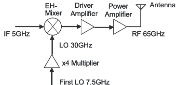
Figure 1 shows the block diagram of 60 GHz-band trans- mitter module with integrated antenna. Input IF signal is 5 GHz-band and is up-converted to 65 GHz by using an even harmonic mixer. Then it is amplified up to 10 dBm by a driver amplifier and a power amplifier. Since the LO signal of 7.5 GHz is used, x4 multiplier is required for the 60 GHz- band even harmonic mixer. All of active circuits are fabri- cated by GaAs MMIC technology. At antenna input, P
1 dB(output power at 1 dB gain compression point) of 6.2 dBm and P
sat(saturated output power) of 12 dBm are obtained.
The output spurious level is 40 dB lower than that of desired signal. The detail of these circuit blocks except antenna and their performances are described in Ref. [11].
Figure 2 shows the structure of antenna integrated transmitter module. The module consists of three sheets of Any Layer Interstitial Via Hole (ALIVH) substrate and GaAs MMIC’s. The ALIVH substrate is produced by Pana- sonic Electric Industrial Co., and is an non-woven organic multilayered substrate. It’s relative permittivity is 3.47 and dielectric loss tangent is 0.032. The top substrate is RF substrate which handles 60 GHz-band RF signal. Mixer, Driver amplifier and power amplifier GaAs-MMIC chips are mounted on the substrate and an planar antenna are integrated in the substrate. The second top substrate is LO substrate which generates 30 GHz LO signal for the
Fig. 1 Block diagram of 60 GHz-band transmitter module with integrated antenna.
Copyright c 2012 The Institute of Electronics, Information and Communication Engineers
Fig. 2 Configuration of 60 GHz-band transmitter module with integrated antenna.
Fig. 3 Cross sectional view of interconnection section of 60 GHz-band transmitter module.
Fig. 4 Enlarged photo and cross sectional view of flip-chip mounted MMIC on ALIVH substrate.
60 GHz-band even harmonic mixer, from a 7.5 GHz LO sig- nal. The bottom substrate is IF substrate which provides 5 GHz IF signals and 7.5 GHz LO signal to RF/LO sub- strates. Since the IF substrate requires RF/D.C. connectors to supply IF/LO signals and D.C. power to the transmitter module, the IF substrate size becomes larger than the trans- mitter module. The effective size of the transmitter module is same as that of RF substrate.
Figure 3 shows the cross sectional view of interconnec- tion section of the module. A GaAs MMIC chip is flip-chip mounted on an ALIVH substrate by using Au Stud Bump Bonding (SBB) with underfill agent. Au bump (height of 50 µ m) is fixed on a organic substrate by conductive ad- hesive. Figure 4 shows the enlarged photo and the cross sectional view of flip-chip mounted MMIC on ALIVH sub- strate. Figure 5 shows the Au-SBB flip-chip process flow.
Since the ALIVH substrate has a MMIC on it’s surface,
Fig. 5 Au-SBB flip-chip process flow.
Fig. 6 Test sample of vertically stacked ALIVH substrates for Cu-ball interconnection evaluation.
Fig. 7 Process flow of Cu-ball interconnection for vertically stacked ALIVH substrates fabrication.
the distance between the vertically stacked ALIVH sub- strates should be more than the thickness of GaAs MMIC (around 300 µm.) To obtain the required height of more than 300 µm, Cu-ball interconnection technology is employed which has been widely used in ball grid array (BGA) pack- aging. In this case, the diameter of Cu-ball was selected as 350 µm. By using EM simulation, ground (GND) pattern and Cu-ball arrangements (number and location) are opti- mized. Figure 6 shows the test sample of vertically stacked ALIVH substrates for Cu-ball interconnection evaluation.
The measured loss of interconnection is less than 1 dB at
60 GHz. Figure 7 shows the process flow of Cu-ball inter-
connection.
Fig. 8 Actual substrate pattern of 60 GHz-band antenna integrated transmitter module with IF substrate.
Fig. 9 EM simulation model of 60 GHz-band transmitter module for antenna design.
3. Antenna Design
Figure 8 shows the actual substrate pattern of 60 GHz-band antenna integrated transmitter module with IF substrate.
Figure 9 shows the EM simulation model of the transmit- ter module which is used for antenna design. A planar dipole antenna is located on the top ALIVH substrate (RF substrate.) In order to simplify the EM simulation, the top metal of IF and RF substrates is considered as GND except antenna element, antenna feed circuit and surrounding area of RF substrate. This means the connectors and MMIC’s mounted on the surfaces of IF / RF substrates can be ignored in antenna design. Figure 10 shows the detailed structure and the dimensions of the planar dipole antenna. A pair of radiators; dipole antenna is patterned on the top-side and on the back-side of the top ALIVH substrate. Since the dielec-
Fig. 11 Simulated return loss of integrated planar dipole antenna.
tric constant of organic substrate, such as ALIVH, is lower than ceramics or semiconductors in general cases, it is suit- able to configure the antenna having wider frequency band- width.
Figure 11 shows the simulated return loss of planar dipole antenna. Bandwidth of 18.2% is obtained in 60 GHz- band. Figure 12 shows the simulated antenna pattern at 63 GHz. Actual gain of 6.8 dBi is obtained. Due to the effect of GND of IF substrate, the direction of main beam becomes theta = 60 degrees.
4. Fabrication and Measurements
Figure 13 shows a photograph of the fabricated 60 GHz- band transmitter module with integrated antenna. The size of RF substrate is 9 mm × 10 mm. On the top of RF sub- strate, three GaAs-MMIC’s (mixer, driver amplifier and power amplifier) are flip-chip mounted. Since the I / O con- nectors are mounted on the IF substrate, the size of IF sub- strate becomes 26.5 mm × 27 mm, but it’s effective area is just the same as RF substrate.
Figure 14 shows the transfer characteristic of fabricated transmitter module. The output power was measured at the antenna feed. P
1 dBof 6.2 dBm and P
satof 12 dBm are ob- tained at 63 GHz. Undesired signals, i.e. LO leakage and image signal are suppressed by the image rejection type even harmonic mixer. LO leakage is less than − 34 dBm and image rejection ratio (IRR) is 55 dB.
Figure 15 shows the measured antenna pattern of fabri-
cated transmitter module. Actual gain of 6.0 dBi is obtained
and agrees with designed value of 6.3 dBi. The measured
antenna pattern is in agreement with the simulated results
and this means that the top of the RF substrate and IF sub-
Fig. 12 Simulated antenna pattern [9].
Fig. 13 Photograph of fabricated 60 GHz-band transmitter module with integrated antenna [9].
Fig. 14 Transfer characteristic of transmitter module at antenna feed.
IF frequency is 5 GHz, LO frequency is 7.25 GHz and RF frequency is 63 GHz. In the figure, USB (upper side band) is desired transmit signal (63 GHz), LO is undesired local signal leakage (58 GHz) and LSB (lower side band) is undesired image signal (53 GHz.) IRR shows image rejection ratio.
strate can be considered as GND in this planar dipole an- tenna design.
5. Conclusions
Targeting 60 GHz-band, small, low cost wireless transceiver, antenna integrated transmitter module using 3-D SiP tech- nology is developed. By using Au-SBB for MMIC flip chip mounting and Cu-ball interconnection for vertically stack- ing of ALIVH substrates, ultra-small size is feasible. By us- ing organic substrates, such as ALIVH substrates, low cost is achievable. Since this substrate has lower dielectric con- stant than LTCC, it causes easy radiation from integrated antenna. Actual gain of 6.0 dBi is obtained by the measure- ment of fabricated antenna integrated transmitter module.
The results show that the proposed 60 GHz antenna in- tegrated module using organic substrates and 3-D SiP tech- nology is very promising.
As the future works, GaAs-MMIC’s should be merged and replaced by a Si-RFIC to achieve higher integration/
lower cost. Active phased array antenna should be also investigated to obtain higher antenna gain and beam scan- ning/forming functionality.
Acknowledgment
The authors would like to thank Core Research for Evo- lutional Science and Technology program (CREST) of Japanese Science and Technology Agency (JST) for the fund support.
References
[1] S. Emani, R.F. Wiser, E. Ali, M.G. Forbes, M.Q. Gordon, X. Guan, S. Lo, P.T. McElwee, J. Parker, J.R. Tani, J.M. Gilbert, and C.H.
Doan, “A 60 GHz CMOS phased-array transceiver pair for multi- Gb/s wireless communications,” IEEE ISSCC 2011, pp.164–165,
Fig. 15 Measured antenna pattern of fabricated module [9].
2011.
[2] T.-W. Huang and H. Wang, “Millimeter-wave CMOS integrated cir- cuits for gigabit WPAN applications,” IEEE CICC 2008, pp.228–
231, 2008.
[3] K. Kan, F. Lin, D.-D. Pham, J. Brinkhoff, C.-H. Heng, Y.X. Guo, and X. Yuan, “A 60-GHz OOK receiver with an on-chip antenna in 90 nm CMOS,” IEEE J. Solid-State Circuits, vol.45, no.9, pp.1720–
1731, 2010.
[4] K. Maruhashi, M. Ito, S. Kishimoto, and K. Ohata, “60-GHz- band LTCC module technology for wireless gigabit transceiver ap- plications,” 2005 Int. Workshop on Radio-Freq. Integration Tech., pp.131–134, Dec. 2005.
[5] F. Wollenschlager, L. Alhouri, L. Xia, S. Rentsch, J. Muller, R.
Stephan, and M.A. Hein, “Measurement of a 60 GHz antenna ar- ray fed by a planar waveguide-to-microstrip transition integrated in low-temperature co-fired ceramics,” Proc. 3rd Eur. Conf. on Anten- nas and Propagation, pp.1001–1005, April 2009.
[6] T. Seki, N. Honma, K. Nishikawa, and K. Tsunekawa, “Millimeter- wave high-efficiency multilayer parasitic microstrip antenna array on teflon substrate,” IEEE Trans. Microw. Theory Tech., vol.53, no.6, pp.2101–2106, June 2005.
[7] S. Yoshida, S. Kameda, T. Takagi, and K. Tsubouchi, “Radia- tion characteristics of a planar monopole antenna integrated with a 60 GHz band WPAN module using organic substrates,” 4th Euro- pean Conference on Antennas and Propagation (EuCAP), C33P1-5, April 2010.
[8] S. Yoshida, K. Tsubouchi, A. Tosaki, H. Oguma, S. Kameda, H.
Nakase, and T. Takagi, “Radiation charatceristics of ultra-small wireless communication modules for 60 GHz band WPAN,” 2008 IEEE Antennas and Propagation Society Int. Symposium (AP-S 2008), July 2008.
[9] N. Suematsu, S. Yoshida, S. Tanifuji, S. Kameda, T. Takagi, and K.
Tsubouchi, “60 GHz antenna integrated transmitter module using 3- D SiP technology and organic substrates,” 41st European Microwave Conference (EuMC), pp.551–554, Oct. 2011.
[10] K. Tsubouchi, M. Yokoyama, and H. Nakase, “A new concept of 3-dimensional multilayer-stacked system-in-package for software defined-radio,” IEICE Trans. Electron., vol.E84-C, no.12, pp.1730–
1734, Dec. 2001.
[11] K. Masuda, F. Takeuchi, Y. Hamada, K. Maruhashi, H. Oguma, S.
Kameda, H. Nakase, T. Takagi, and K. Tsubouchi, “60-GHz-band transmission module for 3-dimensional system-in-package,” Proc.
2006 8th Electron. Packaging Tech. Conf., pp.90–95, Dec. 2006.
[12] H. Nakase, T. Fujii, S. Oshima, H. Oguma, S. Kameda, Y. Isota, and K. Tsubouchi, “Evaluation of high frequency characteristics of ALIVH substrate for 60 GHz RF modules,” Proc. 2006 8th Electron.
Packaging Tech. Conf., pp.639–642, Dec. 2006.
[13] S. Yoshida, S. Tanifuji, S. Kameda, N. Suematsu, T. Takagi, and K. Tsubouchi, “Copper balls interconnection technology for 60 GHz band 3-D system-in-package modules,” 2010 Asia-Pacific Microwave Conference (APMC2010), TH3F-1, Dec. 2011.
[14] S. Yoshida, S. Tanifuji, S. Kameda, N. Suematsu, T. Takagi, and K. Tsubouchi, “60-GHz band copper ball vertical interconnection for MMW 3-D system-in-package front-end modules,” IEICE Trans.
Electron. (to be published.)
[15] S. Yoshida, H. Oguma, S. Kameda, T. Takagi, and K. Tsubouchi, “A fundamental study of antennas for 60 GHz band ultra-small WPAN modules using organic resin substrates,” IEICE Trans. Commun.
(Japanese Edition), vol.J93-B, no.6, pp.822–831, June 2010.
microwave and millimeter-wave solid-state cir- cuits including MMIC’s/RFIC’s and linearizers for various wireless applications. From 1992 to 1993, he was a visiting researcher at the University of Leeds, Leeds, U.K.
He is currently a professor at the Research Institute of Electrical Commu- nication, Tohoku University, Sendai, Japan. Professor Suematsu has been a steering committee member of IEEE RFIC symposium and his current interests are in RF CMOS devices and systems for broad-band wireless in- formation technologies. He is a senior member of the IEEE, and a member of the Japan Society of Applied Physics.
Satoshi Yoshida was born in Saga, Japan, in 1984. He received the B.S. and M.S. degrees in electrical and communication engineering from Tohoku University, Sendai, Japan in 2007 and 2009, respectively. He is currently working to- ward the Ph.D. degree in electrical and commu- nication engineering in Tohoku University, Sen- dai, Japan. His main research interests include small antennas, multiple antenna systems, and millimeter-wave antenna systems.
Shoichi Tanifuji was born in Gunma, Japan.
He received the B.S., M.S. and Ph.D. degrees in electrical and communication engineering from Tohoku University, Sendai, Japan in 2006, 2007 and 2010, respectively. He is currently the Re- search Fellow of the Research Institute of Elec- trical Communication, Tohoku University. His current interests are in digital RF circuits, dig- itally assisted RF analog circuits, broadband wireless on-chip transceivers, GHz-band SAW
& BAW signal processing devices and materials for mobile broadband wireless access network.
Suguru Kameda was born in Fukushima, Japan, 1974. He received the B.S., M.S., and Ph.D. degrees in electronics engineering from Tohoku University, Sendai, Japan, in 1997, 1999, and 2001, respectively. He is currently the Associate Professor of the Research Institute of Electrical Communication, Tohoku Univer- sity. His current interests are in heterogeneous network, CDMA, and OFDMA for mobile com- munication networks, and RF signal processing integration circuits. He received the TELECOM System Technology Award for Students in 2001, the special prize selected by judge of EDS-Fair 2005, and 2008 Young Investigator Award in Soft- ware Radio in IEICE Technical Committee on Software Radio. He is a member of the IEEE.
nology. Since 2005, he has been a professor of Research Institute of Electrical Communication, Tohoku University. He is now a visiting profes- sor. His main area of research interest is mobile wireless broadband com- munication circuits and systems technology. He is a senior member of the IEEE.
Kazuo Tsubouchi was born in Kyoto, Japan, in 1947. He received the B.S., M.S., and Ph.D. degrees in Electronics Engineering from Nagoya University, Nagoya, Japan, in 1969, 1971, and 1974, respectively. Since 1974, he has been with the Research Institute of Elec- trical Communication, Tohoku University, Sen- dai, Japan. In 1982, he worked at Purdue Uni- versity as a Visiting Associate Professor. He is currently the Professor Emeritus of Tohoku University. His current interests are highly re- liable GHz-band wireless communication system, GHz-band surface and bulk acoustic wave devices and materials, low-power RF signal processing integration circuits, high speed Si CMOS circuit/device/process technol- ogy, and system in package (SiP) technology. Prof. Tsubouchi received the Hattori-Hoko Award in 1983, the 26th Ichimura Award in 1994, the TELE- COM System Technology Award in 1996, the 22nd Inoue Harushige Award in 1997, the 2005 Achievement Award from the IEICE, and “Minister of Education, Culture, Sports, Science and Technology Award” in the Award for Persons of Merit in Industry-Academia-Government Collaboration in FY2007. He is a member of the IEEE, the Physical Society of Japan, the Japan Society of Applied Physics, and the Institute of Electrical Engineers of Japan.
![Fig. 13 Photograph of fabricated 60 GHz-band transmitter module with integrated antenna [9].](https://thumb-ap.123doks.com/thumbv2/123deta/5626740.1500332/4.892.119.386.786.1013/fig-photograph-fabricated-ghz-transmitter-module-integrated-antenna.webp)
![Fig. 15 Measured antenna pattern of fabricated module [9].](https://thumb-ap.123doks.com/thumbv2/123deta/5626740.1500332/5.892.132.763.121.465/fig-measured-antenna-pattern-fabricated-module.webp)
