of spin‑orbit interaction in ZnO
著者 モハマド アドヒブ ウリル アブソル
著者別表示 Moh Adhib Ulil Absor journal or
publication title
博士論文本文Full 学位授与番号 13301甲第4311号
学位名 博士(理学)
学位授与年月日 2015‑09‑28
URL http://hdl.handle.net/2297/43824
doi: 10.7567/APEX.7.053002
Creative Commons : 表示 ‑ 非営利 ‑ 改変禁止 http://creativecommons.org/licenses/by‑nc‑nd/3.0/deed.ja
Dissertation
Density-functional theory based calculations of spin-orbit interaction in ZnO
Author:
Moh. Adhib Ulil Absor 1223102008
Supervisor:
Prof. Mineo Saito
A Dissertation submitted in fulfilment of the requirements for the degree of Doctor of Science (D.Sc)
in the
Graduate School of Natural Science and Technology Kanazawa University
September 2015
Tunable Rashba Effect on Strained ZnO: First-principles density-functional study, Applied Physics Express Vol 7, pp. 053002 (2014).
2. Moh. Adhib Ulil Absor, Fumiyuki Ishii, Hiroki Kotaka, and Mineo Saito, Persistent spin helix on ZnO (1010) surface: first-principles density functional study, Applied Physics Express Vol 8, pp. 073006 (2015).
Abstract
Graduate School of Natural Science and Technology Division Mathematical and Physical Science
Doctor of Science by Moh. Adhib Ulil Absor
Recently, the field of spintronics attracted much attention because of their po- tential application in future electronic devices. The new scheme of spintronics utilizing the effect of spin-orbit interaction (SOI) on the spin textures has been extensively studied. Here, two dimensional electron gas (2DEG) system is an ideal platform because it can be controlled by applying an external electric field or by introducing strain. Wurtzite ZnO is promising materials candidate for spintron- ics since the high quality of the 2DEG system has been experimentally observed.
Therefore, it is crucially important to clarify the effect of SOI in this material, which is expected to induce useful properties for spintronics applications.
In this dissertation, the effect of SOI is studied by using first-principles density- functional theory (DFT). We calculate the spin textures to identify physical prop- erties induced by the SOI. Here, we investigate two different systems, which are (i) the bulk system, and (ii) the surface system oriented on the [1010] direction.
In the case of bulk system, we find that strain controls SOI, where the inversion Rashba rotations are identified. We revealed that the spin-orbit strength can be effectively controlled by tuning the strain. On the other hand, in the case of the surface system oriented to the [1010] direction, we in the first time find that the SOI leads to the novel system called as the persistent spin helix (PSH), exhibiting a quasi-one dimensional orientation of the spin textures. We find that the wavelength of this PSH is smaller than that observed on various zinc-blende quantum well structures.
Finally, we conclude that both the strained bulk and the surface systems are promising for spintronics applications.
On this page, I wish to express my sincere gratitude to my supervisors, Prof.
Mineo Saito and Prof. Fumiyuki Ishii, for their motivation, support and guidance during my study. They have given me an opportunity and complete freedom to work on interesting research topics during the last three years. This thesis is a result of their consistent encouragement and the fruitful discussions I had with them.
I am thankful to the Directorate General of Higher Education (DIKTI), Indonesia, and Kanazawa University, Japan, for financial support through the Joint Scholar- ship Program.
I give thanks to all of computational science research group members, especially for Dr. Hiroki Kotaka who teachs me about practical computational based-density- functional theory (DFT) calculations used in this dissertation. I also would like to thank to my Indonesia friends, especially in Indonesia Student Association Ishikawa (PPI Ishikawa) who are always strengthen and supports me in all condi- tions.
Finally, special thanks to my wife (Fathah Dian Sari) and my children (Alifiah Asma salsabila and Itsna Mutiara Hanifah) for supporting me during my study.
iii
Abstract ii
Acknowledgements iii
Contents iv
List of Figures vi
List of Tables ix
1 Introduction 1
1.1 Motivation . . . 1
1.2 Spin orbit interaction (SOI): A new perspective of spintronics . . . 2
1.3 An overview of spintronics devices based on SOI . . . 3
1.4 The purpose: ZnO as a promising material for spintronics . . . 6
1.5 Outline of Dissertation . . . 7
2 Background: Basic Theory and Computational Methods 9 2.1 Introduction . . . 9
2.2 The spin-orbit interaction (SOI) in solids . . . 9
2.2.1 Rashba Effect . . . 11
2.2.2 Dresselhauss Effect . . . 11
2.2.3 Interplay between Rashba and Dresselhauss SOI: the persis- tent spin helix (PSH) . . . 12
2.2.4 Spin relaxation time . . . 16
2.3 Electronic structure based on the density functional theory . . . 17
2.3.1 Manybody Problems in condensed Matter . . . 17
2.3.2 The Hartree approximation . . . 19
2.3.3 The Hartree-Fock approximation . . . 20
2.3.4 The Density Functional Theory Approximation . . . 21
2.3.4.1 The Hohenberg-Kohn Theorems . . . 21
2.3.4.2 The Kohn-Sham Equations . . . 22
2.3.4.3 The exchange-correlation . . . 26
2.4 Computational Scheme . . . 28 iv
2.4.1 Norm conserving pseudo-potential . . . 28
2.4.2 The pseudo-atomic basis orbitals . . . 30
2.4.3 Non-collinear DFT . . . 31
2.4.4 The spin textures calculations . . . 34
2.4.5 The Berry phase method for the electric polarization calcu- lation . . . 36
3 Rashba effect on strained ZnO 38 3.1 Introduction . . . 38
3.2 Computational detailes . . . 39
3.3 Results and discussion . . . 39
3.3.1 Electronic properties of ZnO . . . 39
3.3.2 Rashba effect on ZnO . . . 42
3.3.3 The effect of strain . . . 45
3.3.4 Tunable Rashba effect by strain . . . 47
3.3.5 Discussion . . . 50
3.4 Conclusion . . . 52
4 Persistent Spin helix on the wurtzite ZnO (1010) surface 54 4.1 Introduction . . . 54
4.2 Computational detailes . . . 55
4.3 Results . . . 57
4.3.1 Structural and electronic properties of ZnO (1010) surface . 57 4.3.2 The effect of spin-orbit interaction (SOI) . . . 59
4.3.2.1 Band splitting and the spin textures . . . 59
4.3.2.2 Group theoretical analyses . . . 60
4.3.2.3 Electric polarization analyses . . . 64
4.3.2.4 Discussion . . . 66
4.4 Conclussion . . . 68
5 Summary 70 5.1 Conclussion . . . 70
5.1.1 Rashba effect on strained ZnO . . . 70
5.1.2 Persistent spin helix on ZnO (1010) surface . . . 71
5.2 Future direction . . . 71
1.1 Generation of spin polarization involving the effect of SOI. Electri- cally injected electron becomes spin polarized through two mecha- nism: (i) spin Hall effect (Black arrows) and (ii) currents-induced spin polarization (red arrows). . . 4 1.2 (a) Prototype of spin field effect transistor proposed by Datta and
Das [29]. (b) Mechanism of the spin precession which is induced by SOI. This spin precession can be controlled by applying gate voltage. 5 2.1 Schematic view of the relativistic motion of electron in the two
difference of reference frame., nuclei (left side) and electron (right side). . . 10 2.2 Schematic representation of the splitting band dispersion and the
k-surfaces of constant energy for pure Rashba SOI (a) and com- bination between Rashba and Dresselhauss SOI (b) with the same spin-orbit strength (αR =β1). . . 13 2.3 Schematic representation of the spin polarization for pure Rashba
SOI (a), Dresselhauss SOI (b), and persistent spin helix (c). . . 15 2.4 Schematic representation of the self-consistent loop for solution
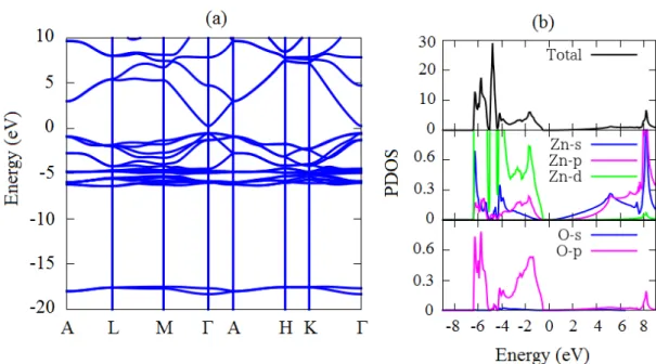
Kohn-Sham equations. . . 25 3.1 Crystal structure of wurtzite ZnO and its first Brillouin zone. . . . 40 3.2 The electronic structures of ZnO. (a) the Band structures and (b)
the density of states projected onto the Zn and O atoms are shown. 41 3.3 (a) Rashba band splitting of the conduction band bottom (CBB) in
around the Γ point and (b) The energy splitting (∆E) as a function of the wave vector in the Γ-K direction (kΓ−K) are shown. The spin textures for (a) the upper and (d) lower bands, which are calculated on 3.5 meV above the degenerate states at CBB, are shown. . . 43 3.4 (a) Schematic view of biaxial strain. The biaxial strain is defined by
the changing in-plane lattice constant a in the two different ways, i.e. tensile biaxial strain (right side) and compressive biaxial strain (left side). (b) Optimized structural parameter (c/a,u) as a function of biaxial strain. The insert shows the thetrahedrally coordiated atoms in the unit cell. d1 represents the bondlength between the Zn and O atoms in the c- direction, while d2 =d3 = d4 define the bondlength of the Zn and O atoms in the non-polar directions. . . . 46
vi
3.5 The band structures of ZnO under different strain condition. The black, blue, and the pink lines represent the band structures of the unstrained, TBS (4%), and CBS (-4%), respectively. . . 47 3.6 The band splitting and the spin textures for different strain con-
dition. The spin textures are calculated on 3.5 meV above the degenerate states of at the CBB. . . 48 3.7 (a) Schematic view of the strain and the Rashba parameter. (b)
Electric polarization difference ∆P, which is calculated by using the Berry phase (BP) method and point charge model (PCM). . . . 49 3.8 Schematic view of the parabolic band dispersion and its properties
is shown. . . 50 3.9 (a) Momentum off-setk0, (b) Rashba eneregy (ER), and the absolut
value of the Rashba parameter (αR) as a function of strain are shown. 52 4.1 (a) The unit cell of the bulk ZnO. The [1010] and [0001] directions
are indicated by the arrow. (b) Top and side views of the slab model of ZnO 1010 surface. The polar direction [0001] is set to be the y directions. The numberN = 1,2,...N indicates the number of bilayer. . . 56 4.2 (a) Brillouin zone of bulk (black lines) and surface systems (blue
lines). (b) The band structure of ZnO (1010) surface (blue lines) projected to those of the bulk system (black lines) are shown. (b) The calculated result of the partial density of states projected onto the surface atoms. . . 58 4.3 Band structures near the VBM in the Y-Γ-X symmetry lines. The
insert shows the spin-split surface-state bands. . . 60 4.4 (a) The brillouin zone of bulk (black lines) and surface (blue lines)
systems. (b) The spin textures of the surface state at VBM. The band energy of the spin textures is 1 meV below the highest en- ergy of the occupied surface state. The arrows represent the spin directions projected to the kx-ky plane. (b) Relationships between rotation angle (φk) and spin components. . . 61 4.5 Expected values of spin projected to the atoms in each bilayer. The
calculations are performed for the spin textures of surface states in Fig. 4.4. The top surface is represented by N=1. . . 62 4.6 Mirror symmetry of the surface, which is seen from the top and side
views. Only one mirror symmetry (y−z plane) is observed in The ZnO (1010) surface. . . 62 4.7 (a) Crystal structure (top and side views) of the bulk system ori-
ented on the [1010] direction. (b) Brillouin zone of the bulk system oriented on the [1010] direction. (c) The spin-split band at the va- lence band maximum (VBM) in the case of bulk system. The insert shows the band splitting of the highest VBM. . . 64 4.8 (a) Spin textures of the the spin-split band at the valence band top
in the case of bulk system. (b) Relationships between rotation angle (φk) and spin components. . . 65
4.9 (a) Calculated data of the in-plane and out-of-plane electric polar- izations ( ∆Py, ∆Pz) in each bilayers. The electric polarizations are calculated by using the PCM. Schematic view of the spin textures and electric fields for the case of the surface (c) and bulk systems (d). . . 66 4.10 (a) Schematic view of the band dispersion along Γ-Xdirection. The
spin-orbit strength of the PSH can be evaluated directly from this band dispersion. (b) Shifting of the two identical Fermi surfaces by the wave vector Q. The wavelenght of the PSH is inversely proportional to the wave vector Q. . . 68 5.1 (a) Crystal structure of hydrogeneted ZnO (1010 surface. (b) band
structure of hydrogeneted ZnO (1010) surface. (c) Density of states projected to the surface atoms. . . 72
3.1 The optimized lattice parameter, which is compared to those of previous calculation and experimental results. . . 40 3.2 The calculated value of the band gap and energy position of the
Zn-d orbitals compared with those of previous calculation and ex- perimental results. . . 41 4.1 The atomic relaxation at the uppermost surface in the out-of-plane
(y) and in-plane (z) direction. . . 57 4.2 Transformation of the polar (kx, ky, kz) and axial vector (σx, σy,
σz) in the symmetry point group Cs. . . 63 4.3 The calculated value of the band gap and energy position of the
Zn-d orbitals compared with those of previous calculation and ex- perimental results. . . 65 4.4 Calculated result of the spin-orbit strenght (αP SH) and wave length
(λP SH) of PSH compared with various zinc-blende quantum well structures. . . 67
ix
Introduction
1.1 Motivation
Recently, the field of spintronics attracted much scientific interest because of their potential applications in future electronic devices [1, 2]. The spintronics or spin electronics refers to the study of the physical properties of electron spin in solid state physics including generation, manipulation, and detection, and also related to the possible devices by exploiting spin in addition to charge degree of freedom.
For example, spin relaxation and spin transport in various metals and semicon- ductors, which recently attracted much attention in both fundamental research and applications [1], are one of the important issues in the spintronics.
The spin, which is the central object in spintronics, was firstly proposed by Pauli in 1925 [3]. As an additional degree of freedom of elementary particles, its nature has been firstly observed by using the Stern-Gerlach experiment [4, 5]. By using the concepts of spin, Fermions with half integer spin can be distinguished from Bosons with integer spin. Therefore, spin plays an important role in determining the basic concepts of the statistics of the elementary particles. The properties of the electron spin can be observed in the systems which rely on magnetism. Here, ferromagnetic materials [6–8], which is recently used in the various electronic devices, is one of the example system showing the appearence of spin in materials.
One of the most important discovery of spintronics is giant magnetoresistance (GMR), which was observed in metallic multilayers by using a spin-dependent electron transport measurement [9, 10]. Recently, the GMR effect has already
1
been used practically in the hard disk drive heads. The discovery of GMR was preceded by the observation of the tunnelling magnetoresistance (TMR) [11–15], which has been realized on the magnetoresistive random-access memory (MRAM) devices. Furthermore, the next generation of the spintronics has been focused on the semiconductor class, such as dilute magnetic semiconductors (DMS), which has been extensively studied [16, 17]. Here, some of new physical properties which is useful for spintronics such as carrier-induced ferromagnetism [18, 19] and pho- toinduced ferromagnetism were found [20–23].
Thus far, recent development of spintronics relies on the new pathway for exploit- ing carrier spins in semiconductors without any addition of magnetic materials or external magnetic fields, which can be realized by utilizing the effect of spin orbit interactions (SOI) on the spin textures[24–29]. This novel approach becomes an alternative way since SOI enables the generation and manipulation of spin solely by electric fields or strain effect. Especially, the Rashba effect [25] attracted much attention because it plays an important role in the spintronics device operation such as the spin-field effect transistor (SFET) [29]. On the other hand, current- induced spin polarization [30] and spin Hall effect [31] are the important examples in spintronics where the SOI has a crucial contribution.
Finally, a part from generation and manipulation of spin polarization, another essential requirement for spintronics devices is a long spin lifetime. Here, a new system known as a persistent spin helix (PSH) atracted much attention [32–39]. In this system, the strongly enhanced spin lifetime is achieved on a certain spatially inhomogeneous spin polarization states [32]. As a result, an efficient spintron- ics devices is believed to be achieved, suggesting that this system is suitable for energy-saving spintronics devices. However, the discovery of the PSH materials has been widely studied only for the zinc-blende semiconductors [32–39]. There- fore, finding another class of materials which is promising candidate for PSH is crucially important in order to realize the PSH based spintronics.
1.2 Spin orbit interaction (SOI): A new perspec- tive of spintronics
Recently, the new scheme of spintronics incorporating the effect of spin-orbit in- teraction (SOI) has been proposed [24–29]. Here, the SOI plays an important role
since it relies to coupling between spin dynamics of an electron and its orbital motion in space. Intuitively, the SOI is a relativistic effect in which an electric field that acts on a fast moving electron is viewed as an effective magnetic field in the reference frame of the electron. Since the SOI induces an effective magnetic field, this study is also known as spintronics without magnetism [24]. In chapter 2, we will present more detail and formal description about the SOI.
In solid state system, the SOI is induced by electric field originated from the lack of space inversion symmetry. Two main cases responsible for lossing the space inversion symmetry: (i) structural inversion asymmetry (SIA) and (ii) bulk inversion asymmetry (BIA). The SIA is induced by the asymmetry of confinement potential of the two dimensional electron gas system in the heterostructures or interface or simply by the presence of surface in a semi-infinite crystal system.
The SOI which is induced by the SIA known as Rashba SOI [25]. On the other hand, BIA which originates from the non-centrosymmetric structure of the crystal induces so called Dresselhauss SOI [28].
In the case of system having both BIA and SIA, it is expected that both Rashba and Dresselhauss types appears. For example, in the two dimensional electron gas (2DEG) system realized on the heterostructure of zinc-blende quantum well (QWs), both Rashba and Dresselhauss SOI are identified, which can be effectively controlled by using an externally electric field via gate voltage [25–27, 29] or by introducing strain effect [40]. Furthermore, it is possible to achieved the condition that the contribution of Rashba and Dresselhauss SOI are equal, which induces a well-known persistent spin helix (PSH), exhibiting the strongly enhanced spin lifetime [32–39]. This situation is in fact observed experimentally in the various zinc-blende QWs system [33–39].
1.3 An overview of spintronics devices based on SOI
In the spintronics device applications, the ability to utilize and controll spin elec- tron is required. Here, generating of spin-polarized currents is one of the central issue [1, 2]. In semiconductors, the generation of spin polarized currents can be realized by using current injection from ferromagnetic materials [16, 17]. Another
Figure 1.1: Generation of spin polarization involving the effect of SOI. Elec- trically injected electron becomes spin polarized through two mechanism: (i) spin Hall effect (Black arrows) and (ii) currents-induced spin polarization (red
arrows).
methods is by using externally applied magnetic fields, which acts as a spin fil- ters to change the unpolarized input currents to be spin-polarized output currents [1, 2]. However, application of external magnetic field in the nonmagnetic system induces stray magnetic field which negatively affects to the spins itself. To over- come this problem, the non-magnetic system which utilize SOI has recently been proposed. In this case, two important mechanism for generating of spin polarized currents have been used such as current induced spin polarization [30] and spin Hall effect [31].
Figure 1.1 shows schematic view of generation spin polarized currents involving the SOI. In semiconductors, electrically-injected electrons become spin polarized through two different mechanisms. First, electron experiences anisotropic scatter- ing from impurity in the presence of SOI, inducing spin accumulation at opposite edges channels with opposite spin direction (black arrows). This mechanism is known as spin Hall effect. The second mechanism, on the other hand, is just currents-induced spin polarization. Here, symmetry-related spin-orbit field pro- duces a homogeneous electron spin polarization throughout the channel(red ar- rows).
Figure 1.2: (a) Prototype of spin field effect transistor proposed by Datta and Das [29]. (b) Mechanism of the spin precession which is induced by SOI. This
spin precession can be controlled by applying gate voltage.
Another important issue in spintronics is the manipulation of spin in semiconduc- tors. Here, the application of external magnetic field becomes one of the methods often used [1, 2]. For a more scalable system, it would be desirable if the SOI is used, which is realized by applying an externally electric field originated from the gate electrode [26, 27, 29] or by introducing strain [40]. In this methods, the tunability of spin manipulation can be realized, which gives an advantage for the future device applications.
The realization of the generation and manipulation of spin by using SOI can be found in the spin-field effect transistor (SFET) device, which is firstly proposed by Datta and Das in 1990 [29]. The idea of this proposal is to inject spin-polarized electrons from a ferromagnetic contact into a one dimensional semiconductor chan- nel in which the electrons travel ballistically to the detection contact. As shown in Fig. 1.2(a), the injected electron originates from feromagnetic source electrode (FM1) starts to rotate because of an effective magnetic field induced by SOI in the 2DEG channel. The electrons can flow when the spin orientation in the 2DEG
is aligned to thos of ferromganetic drain electrode (FM2). On the other hand when spin is flipped in the 2DEG, the electron cannot enters the drain electrode since there is no spin flipped in this electrode [Figure 1.2(b)]. Since the SOI can be effectively tuned by the gate voltage, this indicates that the spin precession is controllable.
1.4 The purpose: ZnO as a promising material for spintronics
Recently, finding new materials which is suitable as a platform for spintronics applications attracted much scientific interest [1, 2]. One of the systems which can be used as an ideal platform for spintronics is two dimensional electron gas (2DEG) system since it can be controlled by an external electric field or by using strain effect. The zinc-blende semiconductor heterostructures supporting 2DEG system becomes one of the promising materials. For example, various 2DEG saterials such as GaAs/AlGaAs [41, 42] and InGaAs/InAlAs [43] heterostructures has been extensively studuied.
The other class of materials which demonstrating 2DEG system comes from ox- ide interface system. This is including LaMnO3/SrMnO3 [44], GaTiO3/SrTiO3 [45], LaAlO3/EuO [46], and LaAlO3/FeS2 [47] in which spin polarized 2DEG has been studied. However, this system has low carrier mobility which is due to the high ef- fective mass of the localizeddbands. Therefore, it is not desirable to use this kind of materials as a particular spintronics application such as high electron mobility transistor (HEMT).
Recently, a different system supporting a 2DEG, wurtzite ZnO interface, has been experimentally observed. Observations of the quantum Hall effect [49] and the fractional quantum Hall effect [50] indicate that ZnO/Zn(Mg)O interface has high quality of the two-dimensional electron gas (2DEG). The high carrier concentra- tions (up to 1013 cm−2) and the high mobility (larger than 105 cm2·V−1·s−1) at low temperature have been reported [50]. Furthermore, the fabrication of the two dimensional electron gas system was also realized in samples grown with metal- organic vapor deposition, which is suitable for mass production [51].
Considering the fact that ZnO-based materials exhibiting the high quality of the 2DEG system, their application as a spintronics materials is plausible. This is supported by the fact that the spin polarization of the 2DEG in ZnO/Zn(Mg)O has been studied [52] and the long spin lifetime has been observed [53, 54]. However, due to the large ionicity and cryatal symmetry, ZnO posses large internal electric fields. This is in fact strongly different compared to the other materials such as zinc-blende semiconductors. Therefore, for spintronics applications, clarification of the SOI in this material is crucially important, which is expected to induce new useful properties for spintronics.
1.5 Outline of Dissertation
This dissertation consists of five chapters. In chapter 1, we present the motivation of this study which is related to the spintronics in general. The new scheme of spintronics based on the spin-orbit interaction (SOI) is given including the generation and manipulation of spin. Here a simple mechanism of the spintronics devices is shown, which is realized on the spin-field effect transitor (SFET).
In chapter 2, we present the basic concepts of the SOI based on the two dimensional electron gas (2DEG) system. The fundamental concepts of density functional theory is also presented. Furthermore, We provide the computational scheme, which is related to the practical calculation in this study.
In Chapter 3, we show the calculated results of the SOI on the strained bulk ZnO. Here we show that strain controls SOI in ZnO, where the inversion Rashba spin rotations are identified. We show that the Rashba spin-orbit strength can be effectively controlled by applying the strain. Finally, we discussed the possible application of the present system for spintronics devices.
In chapter 4, we show the calculated results of the SOI on the wurtzite ZnO (1010) surface. We show that the spin textures show quasi-one dimensional orientation, which is similiar to those of persistent spin helix (PSH). The mechanism which explains the origin of the spin textures is proposed. Furthermore, Some of calcula- tion results of important parameter such as the spin-orbit strength and wavelength of PSH are presented and compare with those various zinc-blende semiconductors.
Finally, in chapter 5, we give a summary and explain the future scope such as the SOI on the metallic surface state of hydrogeneted ZnO(1010) surface.
Background: Basic Theory and Computational Methods
2.1 Introduction
In this chapter, we present the basic theory and methods used in the calculation and analyses. Firstly, we present brief review of the theory of spin-orbit inter- action (SOI) in solids, which is given in Sec. 2.2. Some of interesting physical phemnomena such as the Rashba effect, Dresselhauss effect, and their interplay inducing persistent spin helix (PSH) are presented. Next, in Sec. 2.3, we give a brief review of the electronic structures calculation based on the density functional theory (DFT). Finally, the computational scheme, which is related to the practical calculation, are introduced in Sec. 2.4.
2.2 The spin-orbit interaction (SOI) in solids
Spin-orbit interaction (SOI) is a relativistic effect in which electrons move with a velocity⃗v in the influence of electric field E⃗ created by the nucleus [Figures 2.1].
In the rest frame of the electron, this electric field transforms into a magnetic field
B⃗ =−(⃗v×E)/c⃗ 2, (2.1)
9
Figure 2.1: Schematic view of the relativistic motion of electron in the two difference of reference frame., nuclei (left side) and electron (right side).
where c is the speed of light, that interacts with the magnetic moment ⃗µ of the electron. The energy of the electron in this field is given by
∆E =−⃗µ·B.⃗ (2.2)
Here, ⃗µ = −geµBS/⃗ ~ is the , where ge = 2.002 is the g-factor of the electron, µB = e~/(2me) is the Bohr magneton, me is the electron a free electron, ~ is Planck’s constant, and S⃗ is the electron spin vector. The SOI, then, can be expressed by,
HSOI =− ~
4m2ec2⃗σ·(⃗p×E)⃗ (2.3) where⃗σ= (σx, σy, σz) is the vector of Pauli spin matrices defined as,
σx = (
0 1 1 0
)
, σy = (
0 −i i 0
)
, σz = (
1 0
0 −1 )
(2.4)
In crystal systems, where the total Hamiltonian is invariant under the time reversal symmetry, the energy solution of the Hamiltonian obeys the relation, E(↑, ⃗k) = E(↓,−⃗k), where ↑ and ↓ are the up and down spins, respectively. At the same time, the present of the spatial inversion symmetry of crystal induces E(↑, ⃗k) = E(↑,−⃗k). Spin degeneracy is the consequence of the combination of the time reversal and spatial inversion symmetry, which leads to the fact that the condition
E(↑, ⃗k) = E(↓, ⃗k) is obtained. This condition is known as Kramers’ degeneracy, where the states is non-spin polarized.
When the space inversion symmetry is broken, the spin degeneracy is lifted by the SOI. The loss of space inversion symmetry can either originate from a structural inversion asymmetry (SIA), which induces the Rashba effect [25–27], or from bulk inversion asymmetry (BIA), which induces the Dresselhauss effect [28]. The SIA is induced by the asymmetric confinement potential of the two dimensional electron gas in a semiconductor heterostructure, or simply by the presence of the surface in a semi-infinite crystal, while the BIA originates from the non-centrosymmetric of the crystal structures. In the following section, we will discuss about the Rashba and Dresselhauss types of SOI and their interplay which induces the well-known persistent spin helix (PSH).
2.2.1 Rashba Effect
The Rashba effect has been extensively studied on semiconductor heterostructures in which electrons are confined to the interface [25–27]. Another system exhibiting the Rashba effect is the surface, which is extensively studied on the high quality epitaxial metal layers [55–58]. In the two-dimensional electron gas (2DEG) system under the influence of electric fieldEz perpendicular to the growth plane (2DEG- plane), the Rashba SOI can be expressed by the effective Hamiltonian
HR=− ~
4m2ec2⃗σ·(⃗p×E) =⃗ αR(σxky −σykx) (2.5) where αR=−~Ez/(4m2ec2) is the Rashba spin-orbit strength, kx and ky are wave vectors in the x and y directions, respectively, and σx and σy are Pauli matrixes.
2.2.2 Dresselhauss Effect
In some crystal system with lack a center of inversion, such as the zinc-blende crystal, the Dresselhaus SOI is induced [28], which is expressed by
HD =βD[kx(
ky2−kz2)
σx+ky(
k2z−kx2)
σy +kz(
kx2−ky2)
σz]. (2.6)
Here, βD is the Dresselhauss spin-orbit strength. In semiconductor heterostruc- tures quantum well (QW), where electrons are confined in the z- direction to a two dimensional (x−y) plane, the condition that ⟨kz⟩= 0 and ⟨k2z⟩ ≈(π/d)2 are obtained, wheredis the well width. As a result, the Hamiltonian in Eq. (2.7) can be written in the first and third terms of k, which is expressed by
HD =β1(kxσx−kyσy) +β3[kxky2σx−kykx2σy]. (2.7)
where β1 = βD, = βD(π/d)2 and β3 = βD are the first and third terms of the Dresselhauss spin-orbit strength, respectively.
2.2.3 Interplay between Rashba and Dresselhauss SOI: the persistent spin helix (PSH)
The total Hamiltonian of the SOI incorporated the Rashba and Dresselhauss terms is expressed by
HSOC =αR(σxky−σykx) +β1(kxσx−kyσy) +β3(kxky2σx−kykx2σy) (2.8)
In this Hamiltonian, the Schr¨odinger equation leads to the eigenvalues solution in which two energy braches appears, known as apin-split bands E(k,↑↓). This spin-split bands obey the condition that E(k,↑) ̸= E(k,↓) for k ̸= 0, while it requires E(k,↑) = E(−k,↓) for k= 0 due to the time reversability.
For each k, the spin splitting ∆Esplit(k) is defined as
∆Esplit(k) =E(k,↑)−E(k,↓). (2.9)
For the case of β3 = 0, the eigenvalues of Hamiltonian of Eq. (2.7) leads to the band dispersion:
E(k,↑↓) = ~2k2
2m∗ ±kζ(αR, β1, θk), (2.10) where ζ(αR, β1, θk) is defined as
Figure 2.2: Schematic representation of the splitting band dispersion and the k-surfaces of constant energy for pure Rashba SOI (a) and combination between Rashba and Dresselhauss SOI (b) with the same spin-orbit strength (αR=β1).
ζ(αR, β1, θk) =
√
α2+β12+ 2αRβ1sin 2θk. (2.11)
In this expression,θkis defined in thekx−kyplane by the relation,k= (|k|cosθk,|k|sinθk. For the case of pure Rashba SOI, the band dispersion in Eq. (2.10), leads to the
well-known Rashba dispersion:
E(k,↑↓) = ~2k2
2m∗ ±αRk. (2.12)
In this band dispersion, the spin splitting energy, ∆Esplit(k), is linear in k along any direction. This splitting is isotropic where k-surfaces of constant energy are concentric circles centered at k = 0 [Figure 2.2(a)]. When we introduce the Dres- selhauss SOI, on the other hand, the Eq. (2.10) leads to anisotropic of the spin splitting ∆Esplit(k) [Figure 2.2(b)].
An interesting case is obtained when αR =β1. In this case, a novel system called as persistent spin helix (PSH) is achieved [32]. Here, energy band dispersion in Eq. (2.10) reduces to be
E(k,↑↓) = ~2k2
2m∗ ±2αRk+, (2.13)
where k+= (kx+ky)/√
2. This PSH band dispersion has the shifting properties,
E(k,↑) = E(k+Q,↓). (2.14)
Here, Q=Q+ = 4mαR is the shifting wave vector. In this PSH band dispersion, k-surfaces of constant energy consist of two circles shifted by the wave vector Q [Figure 2.2(b)].
The eigen energies ofE(k,↑↓) in Eq. (2.10) corresponds to the eigenstate [59]
Ψ(k,↑↓) = exp(i(k·r))
√2
( iexp(−iφ(k))
±1
)
(2.15)
where the function φ(k) obeys the relation,
exp(−iφ(k)) = αRexp(−iθk)−iβ1exp(−iθk)
ζ(αR, β1, θk) (2.16) Subsequently, by using Eq. (2.15) the spin polarization can be evaluated by cal- culating the expected value of spin using the expression,
P↑↓=⟨Ψ(k,↑↓)|S|Ψ(k,↑↓)⟩=
∓sinφ(k)
±cosφ(k) 0
(2.17)
For the case of pure Rashba SOI, we have φ(k) = θk. In this case, the spin polarization in Eq. (2.17) leads to the expression
Figure 2.3: Schematic representation of the spin polarization for pure Rashba SOI (a), Dresselhauss SOI (b), and persistent spin helix (c).
P↑↓=
∓sinθk
±cosθk 0
(2.18)
In the case of PSH (αR=β1), we find thatφ(k) =π/4, then the spin polarization in Eq. (2.17) leads to the form
P↑↓=
∓√12
±√12 0
(2.19)
Figure 2.3 shows the spin polarization for several cases. For the case of pure Rashba or Dresselhauss SOI, the spin polarization is k-dependent [Figure 2.3 (a) and (b)]. this leads to the fact that the spin polarization decays implying the shorter spin relaxation time. On the other hand, in the case of PSH, the spin polarizations show one dimensional orientation, which is independent tok [Figure 2.3 (c)]. This leads to the fact that spins do not precess, suppresing the decay of spin polarization, which induces the strongly enhanced spin relaxation time [32].
2.2.4 Spin relaxation time
One of the important consequences of SOI is the spin relaxation time. In the classical picture of the electron, a single spin⃗s⃗k propagates along certain direction with the velocity ~m⃗k and precesses around magnetic field B⃗⃗k induced by the spin- orbit interaction (SOI), the precession of the ballistically propagating single spin is expressed by
d⃗s⃗k
dt =Ω⃗⃗k×⃗s⃗k (2.20)
where ⃗Ω⃗k is the precession frequency defined as ⃗Ω⃗k = gµB~B⃗⃗k. The term of B⃗⃗k in the precession frequency can be understood by expressing the SOI Hamiltonian in term of Zeeman spin splitting,
HSOI = gµBB⃗⃗k
~ ·S⃗ (2.21)
Inserting Eq. (2.21) into Eq. (2.8) and setting thatβ3 = 0, the effective magnetic field can be expressed by
B⃗⃗k = 2k gµB
( αRsinθ+β1cosθ
−αRcosθ−β1sinθ )
(2.22)
In the case of diffussion limit, where the effective momentum scattering time (τp∗) is much smaller than the time for fully spin rotation, the spin travels random walk on the Bloch sphere. In this situation, the spin polarization decays through D’yakonov-Perel’ mechanism [60], where the decay rate is expressed as
1
τx =τp∗⟨ Ω2x⟩
(2.23)
1
τy =τp∗⟨ Ω2y⟩
(2.24)
1
τz =τp∗⟨
(Ω2x+ Ω2y)⟩
(2.25)
Here, τx, τy, and τz denote the spin life time for a spin polarization along x-, y-, and z-directions, respectively. For the case of pure Rashba SOI (β1 = 0), the Rashba spin-orbit field induces the precession of the spin where the spin life time decreses by increasing of the quadratic αR. This indicates that the large Rashba spin-orbit strength αR significantly reduces the spin life time. On the contrary, in the case of the persistent spin helix (αR = β1), the effective spin-orbit field is unidirectional, which leads to the fact that the spin do not precess, inducing the strongly enhanced spin life time [32].
2.3 Electronic structure based on the density func- tional theory
In the real system, the simplified Hamiltonian mentioned before cannot describe correctly the effect of SOI. This is due to the fact that the interaction between the electrons and also nuclei plays an important role. Indeed, for the case of materials that contains atoms of high Z (atomic number), SOI has significant contribution of their electronic properties. Since in the complex system, understanding of the SOI involves many body interactions, the study of the electronic properties of the interacting systems is important. Here, the density functional theory (DFT) based methods is the powerfull tool to describe the correct understanding of the electronic properties incorporating the effect of SOI. The brief review of the DFT scheme are given in the following sub-sections.
2.3.1 Manybody Problems in condensed Matter
In condensed matter physics, the origin of the various material properties can be understood by identifiying the interaction of electrons. Here, a detailed un- derstanding of electronic structure is the most importance knowledge. To reach detailed knowledge about the electronic structure, a valid quantum-mechanical description of the physical properties of materials is required. In the complex system consisting of many electrons and nuclei, the Schr¨odinger equation can be expressed as
HΨ(r1,r2, ...,R1,R2, ...) = EΨ(r1,r2, ...,R1,R2, ...) (2.26)
where Ψ is the wave function of the system, ri and Ri are the positions of the electrons and ions respectively, and H is the Hamiltonian of the system, which is expressed in the form
H =−∑
i
∇2i
2 −∑
i,I
ZI
|ri−RI|+1 2
∑
i̸=j
1
|ri−rj|−∑
I
∇2I
2MI+1 2
∑
I̸=J
ZIZJ
|Ri−Rj| (2.27)
where MI and ZI are the nucleus mass and charge, respectively. Here, we use the atomic units, where ~ = me = e = 4πϵ0 = 1. Furthermore, the Hamiltonian in Eq. (2.27) can be decomposed into five terms
H =Tel+Vel−nuc+Vel−el+Tnuc+Vnuc−nuc (2.28)
where Tel and TN are the kinetic energy operator of electrons and nuclei respec- tively, Vel−nuc is the potential energy of the electrons relative to the nuclei, Vel−el represents the Coulomb interaction between the electrons, and similarly, Vnuc−nuc is the Coulomb interaction between nuclei.
The Eq. (2.26) is defined in 3M + 3N-parameter space dimension, which is too complex to be solved except for the simplest system such as the hydrogen atom.
For the larger systems such as molecules and solids, additional approximations have to be used. Considering the fact that the mass of the nuclei is much larger than those of the electron, the motion of nuclei is negligible compared to those of the electrons. Therefore, from the electron point of view, the nuclei move stationary and fix their positions. This approximation is known as the Born- Oppenheimer approximation.
In this approximation, TN and Vnuc−nuc in Eqs. (2.28) can be ignored and the Hamiltonian in Eq. (2.28) can be simplfied by
H =Tel+Vel−el+Vel−nuc (2.29)
The Schr¨odinger equation of this system now can be expressed as
HΨ = [
−∑
i
∇2i 2 + 1
2
∑
i̸=j
1
|ri−rj| −∑
i,I
ZI
|ri −RI| ]
Ψ =EΨ (2.30)
where Ψ = Ψ(r1,r2, ...) is many electron wave function. We can see that the original problem is now reformulated as a quantum many-body problem for the electrons in an Hamiltonian set by the nuclei positions.
2.3.2 The Hartree approximation
The simplest method to solve the many-electron equation is to rewrite Eq. (2.29) as a one-particle equation for an electron moving in an average potential of all the electrons. This method is well known as the Hartree approximation [61]. In this methods, the wave function can be written as a product ofn independent electron wave functions ϕ(rn) as follows
Ψ(r1,r2, ...,rn) =ϕ(r1)ϕ(r2)...ϕ(rn) (2.31)
By employing the variational principle, if E0 is the ground state energy solution of the the Schr¨odinger equation, the condition that
⟨ϕ|H|ϕ⟩
⟨ϕ|ϕ⟩ ≥E0 (2.32)
is obtained for any wave function ϕ. By inserting Eq. (2.31) to Eq. (2.30), we can obtaine the Hartree equation:
[−∑
i
∇2i
2 −∑
i,I
ZI
|ri−RI| +∑
i̸=j
∫
ϕ∗j(rj) 1
|ri−rj|ϕj(rj)]ϕi(ri) =ϵiϕ∗iri. (2.33)
In Eq. (2.33), each electroniis treated independently but in an effective potential, which is determined by an integration over the wave function of the other electron.
Since for theith wave function, the effective potential depends on all of other wave functions, we can solve Eq. (2.33) by using the self consistent method. In this
methods, the wave function for the step k can be found by solving the Eq. (2.33) with the effective potential is determined by the wave function in step of k −1.
This procedure is repeated untill all of the wave functions converge to a solution.
2.3.3 The Hartree-Fock approximation
In the Hartree approximation, the exchange interaction is not included in the cal- culation since only symmetric wave functions are used. Therefore, this calculation does not satisfy Pauli exclusion principle. Hartree and Fock in 1926 [62] introduce an approximation methods which deals with electron as a distinguishable parti- cles. Therefore, the system with n-electron wave function is approximated by the anti-symmetric wave function, which described by a Slater determinant [63]:
Ψ(r1,r2, ...,rn) = 1
√n!
ϕ1(r1) ϕ2(r2) · · · ϕn(rn) ϕ1(r2) ϕ2(r2) · · · ϕn(r2)
... ... . .. ... ϕ1(rn) ϕ2(rn) · · · ϕn(rn)
(2.34)
By applying variational principle with this Slater determinant, the solution can be obtained by solving the Hartree-Fock equation:
[−∑
i
∇2i
2 −∑
i,I
ZI
|ri−RI| +∑
i̸=j
∫
ϕ∗j(rj) 1
|ri−rj|ϕj(rj)]ϕi(ri)−
∑
j
[
∫
ϕ∗j(rj) 1
|ri−rj|ϕi(rj)]ϕj(ri) =ϵiϕ∗iri (2.35)
It is clearly seen that the new term appears in the Hartree-Fock equation, which is called as a exchange potential. However, in this equation, the correlation energy due to many body interaction is ignored, which produces incorrect description of the electronic properties. Therefore, the methods which incorporates the effect of both exchange and correlation is necessary.
2.3.4 The Density Functional Theory Approximation
As mentioned before that the electronic structure of the many body system can be described by incorporating the effect of both exchange and correlation. There- fore, an efficient computational practicable scheme is necessary. Recently, DFT is one of the most popular and successful quantum mechanical approaches to de- scribe matter, which is recently applied for calculating, e.g., the binding energy of molecules in chemistry and the electronic band structure of solids in physics.
The idea of DFT is to describe interacting electron system in the form of electron density. This idea is based on the two theorems, which is proposed by Hohenberg and Kohn[64]. The details of the Hohenberg-Kohn are given in the next section.
2.3.4.1 The Hohenberg-Kohn Theorems
There are two theorems porposed by Hohenberg and Kohn[64], which is used as a basis of modern theory of DFT. The first theorem states that the many-body wave functions, which is a central quantity in standar quantum theory, are replaced by using the ground states electron density without any loss of information. This theorem justified that the electron density is the central quantity to find any information of electronic properties. The second theorem give a guidance for the practical computational, which is equaivalent to the variational principles in quantum mechanics.
For the system consists of n electrons, the electron density is defined by using the wave function, which is expressed as
n(r) =
∑N i=1
∫
· · ·
∫
dr1· · ·drNΨ∗(r1,· · · ,rN)δ(ri−r)Ψ(r1,· · · ,rN) (2.36)
This equation leads to the fact that the energy can be rewritten as a functional of electron density but not explicitly the wave function.
The original Hohenberg-Kohn theorems are:
Theorem 1. For any system of interacting particles in an external potential Vext(r), the potentialVext(r)is determined uniquely, except for a constant, by the ground state density n0(r).
This first theorem implies that all of the electronic properties can thus be extracted from the exact ground state electron density. The ground state electron density can be found by applying the second theorem, which is based on the variational principle.
Theorem 2. A universal functional for the energy E[n] in terms of the density n(r) can be defined, valid for any external potential Vext(r). The exact ground state energy of the system is the global minimum of this functional and the density that minimizes the functional is the exact ground state density n0(r).
The second theorem reduces the complex problem to find all of ground state phys- ical properties of a system by minimizing the energy with respect to the electron density. The energy functional as expressed by
EHK[n] =T[n] +Eint[n] +
∫
Vext(r)n(r)dr+EN (2.37)
whereEHK[n] is the total energy functional,T[n] is kinetic energy part, andEint[n]
is the electron interactions energy. In Eq. (2.37)EN is independent to the density, which is due to the nuclei-nuclei interaction. It should also be noted that using the Hohenberg-Kohn formulation of DFT implies that we are working at T = 0 K.
2.3.4.2 The Kohn-Sham Equations
Kohn-Sham reformulated the problem in a more familiar form, which opens way to the practical applications of DFT. Kohn and Sham have shown that there is a way to map the problem of solving Eq. (2.37) to those of a system with non-interacting electrons under an effective potential contributed from all of the other electrons[65].
According to Theorem 2, the true electron density will minimize the total energy, which could be guessed, or, as suggested by Kohn and Sham, calculated from a reference system of non-interacting electrons moving in an effective potential.
For a system with non-interaction electrons, the ground state charge density is represented as a sum over one-electron orbitals,
n(r) = 2
∑N i
|Ψ(r)|2, (2.38)
where i runs from 1 to N/2 for the case of double occupancy of all states. The electron density n(r) can be varied by changing the wave function Ψ(r) of the system.
The Kohn-Sham methods is based on replacing electron interaction by using non- interaction electrons, which is under influence of an effective potential[65]. The effective potential consists of the external potential, the Coulomb interaction be- tween electron, and the exchange and correlation interactions. Therefore, the Kohn-Sham energy functional for the ground state can be expressed by
EKS[n(r)] =Ts[n(r)] +EH[n(r)] +EXC[n(r)] +
∫
Vextn(r)dr (2.39)
In Eq. (2.39), The first term is the kinetic energy of non-interaction electrons, which is expressed by
Ts[n(r)] =−∑
i
∫
Ψ∗i(r)∇2Ψi(r)dr, (2.40)
the second term represented the Hartree energy, which is contains the electrostatic interactio between cloud charge, which is defined as,
EH[n(r)] = 1 2
∫ n(r)n(r’)
r−r’ drdr’, (2.41)
and the third term is the exchange and correlation terms, which are groupped into exchange-correlation energies EXC. When all of the functional EXC[n(r)] is known, the exact ground state density and the energy of the many body system can be found.
Considering the fact that the Khon-Sham energy problem is a minimization prob- lem with respect to the density n(r), the solution can be obtained by performing functional derivative as below
δEKS
δΨ∗i(r) = δT[n]
δΨ∗i(r) + [δEext[n]
δn(r) +δEH[n]
δn(r) +δEXC[n]
δn(r) ] δn(r) δΨ∗i(r)− δ(λ(∫
n(r)dr−N))
δn(r) [ δn(r)
δΨ∗i(r)] = 0, (2.42)
where λ is the Lagrange multiplier. In Eq. (2.42), the last term is the Lagrang multiplier for handling the constrain. Therefore, the non-trivial solution can be obtained.
the second term of Eq. (2.32) indicates that all of potentials such as the exter- nal, Hartree, and the exchange-correlation potentials are expressed in the form of derivative functional so that
Vext = δEext[n]
δn(r) , VH = δEH[n]
δn(r) , VXC = δEXC[n]
δn(r) . (2.43) By setting that
δn(r)
δΨ∗i(r) = 2Ψi(r), (2.44)
each term in the right side of Eq. (2.42) can be expressed as
δT[n]
δΨ∗i(r) =−∇2Ψi(r), (2.45)
[δEext[n]
δn(r) +δEH[n]
δn(r) +δEXC[n]
δn(r) ] = 2(Vext+VH +VXC(r))Ψ∗i(r) (2.46)
δ(λ(∫
n(r)dr−N))
δn(r) [ δn(r)
δΨ∗i(r)] = 2ϵiΨ∗i(r). (2.47) By inserting Eqs. (2.45), (2.46), and (2.47) to Eq. (2.42), we obtained the well- known Kohn-Sham equation
[−1
2∇2+VKS(r)]Ψi(r) = Ψi(r) (2.48)
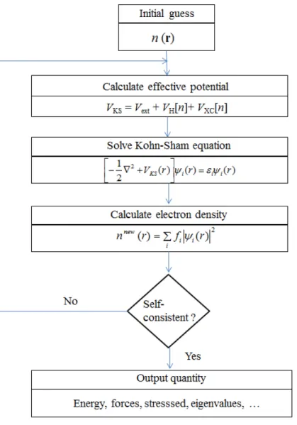
Figure 2.4: Schematic representation of the self-consistent loop for solution Kohn-Sham equations.
where
VKS(r) =Vext(r) +VH(r) +VXC(r) (2.49)
Since bothVext(r) andVH(r) depend onn(r), it is indicate that they also depend on Ψi(r). As a result, the problem solving of the Kohn-Sham equation can be obtained by using the self-consistent methods. The self-consistent Kohn-Sham equation is schematically given in Fig. 2.4. It is usually started from an initial guess of n(r), then calculates the corresponding VH and VXC to obtain VKS. Subsequently, the solution of Ψi can be obtained by solving the Kohn-Sham equation. From this calculation, a new density, which is obtained by the results of Ψi, is used as an

![Figure 1.2: (a) Prototype of spin field effect transistor proposed by Datta and Das [29]](https://thumb-ap.123doks.com/thumbv2/123deta/5640703.2003356/16.893.176.810.122.582/figure-prototype-spin-field-effect-transistor-proposed-datta.webp)