九州大学学術情報リポジトリ
Kyushu University Institutional Repository
Development of RF Energy Harvesters for Low Power Wireless Sensor Networks
モハメド, マガワリー, シェハタ, マンスール
https://doi.org/10.15017/2534463
出版情報:九州大学, 2019, 博士(工学), 課程博士 バージョン:
権利関係:
Development of RF Energy Harvesters for Low Power Wireless Sensor Networks
A THESIS
Submitted to the Graduate School of Information Science and Electrical Engineering
Kyushu University
In Partial Fulfillment of the Requirements for the Degree of
Doctor of Philosophy
in
Electronics and Communication Engineering
By
Mohamed M. Mansour
2019
Development of RF Energy Harvesters for Low Power Wireless Sensor Networks
Submitted by
Mohamed M. Mansour
For The Degree of
Doctor of Philosophy
in
Electronics and Communication Engineering
Examiners,
• Supervisor : Professor Haruichi Kanaya, Dr. Eng
• Co-supervisor 1: Professor Koji Inoue, Dr. Eng
• Co-supervisor 2: Professor Yoshitomi Kuniaki, Dr. Eng
Development of RF Energy Harvesters for Low Power Wireless Sensor Networks
Submitted by Mohamed M. Mansour
For The Degree of
Doctor of Philosophy
in
Electronics and Communication Engineering
To Whom It May Concern, We hereby certify that this print is a typical copy of the original Dr.
Eng. (Doctor of Engineering) thesis ofMr. Mohamed Mansour
Dissertation Title:
DEVELOPMENT OF RF ENERGYHARVESTERS FOR LOWPOWER WIRELESSSENSOR
NETWORKS
Supervisor,
Prof. Haruichi Kanaya, Dr. Eng.
Department of Electronics,
Graduate School of Information Science and Electrical Engineering, KYUSHUUNIVERSITY
2019
Summary
The environment represents a relatively good source of available energy compared with the energy stored in batteries or supercapacitors. In this prospective, energy harvesting, also known as power harvesting and energy scavenging, is an alternative process for primary batteries, where energy is obtained from the ambient environ- ment. An energy harvester typically captures, accumulates, stores, and manages ambient energy in order to convert it into useful electrical energy for autonomous wireless sensor networks. The use of energy scavenging minimizes maintenance and cost operation; therefore, batteries can be eventually removed in the wireless sensor networks (WSN) as well as in portable electronic devices.
RF energy is currently broadcasted from billions of radio transmitters around the world, including mobile telephones, hand-held radios, mobile base stations, and television radio broadcast stations. The ability to harvest RF energy, from ambient or dedicated sources, enables wireless charging of low power devices and has re- sulted benefits to product design, usability, and reliability. Battery-based systems can eliminate the battery replacement. Battery-free devices can be designed to op- erate upon demand or when sufficient charge is accumulated. In both cases, these devices can be free of connectors, cables, and battery access panels, and have free- dom of placement and mobility during charging and usage. The obvious attraction of harvesting ambient RF energy is that it is essentially ”free” energy. The number of radio transmitters, especially for mobile base stations and handsets, continues to increase. It is estimated that the number of mobile phone subscriptions has recently surpassed 5 billion users around the globe.
Mobile phones represent a great source of transmitters from which to harvest RF energy, and will potentially enable users to provide power on-demand for a variety of close range sensing applications. Also, consider the number of WiFi routers and wireless end devices such as laptops. In some urban environments, it is possible to detect hundreds of WiFi access points from a single location. At short range, such as within the same room, it is possible to harvest a tiny amount of energy from
a typical WiFi router transmitting at a power level of 50 to 100 mW. For longer range operation, larger antennas with higher gain are needed for practical harvesting of RF energy from mobile base stations and broadcast radio towers. Alternatively, energy can be generated and broadcasted in unlicensed bands such as 868MHz, 915MHz, 2.4GHz, and 5.8GHz when more power or more predictable energy is needed than what is available from ambient sources. At 915MHz, government reg- ulations limit the output power of radios using unlicensed frequency bands to 4W effective isotropic radiated power (EIRP), as in the case of radio frequency identifi- cation (RFID) interrogators.
The main theme of this thesis is to introduce the recent advancement in the energy harvesting research field and develop a new improved performance rectifier circuits.
Different topologies were suggested and implemented and the conversion efficiency of each technique was derived and plotted to show the incremental improvement compared with other published works. Three major rectifier circuits were studied based on the operating bandwidth and the impedance matching bandwidth.They are, single-band rectifier, broad-band, and differential rectifier topology. Each chapter in the thesis is discussing certain type of the previous configurations. The final chapter provides a practical application for the energy harvesting in the real life. The developed rectifier circuit along with the antenna find an application in the WSN and WBSN.
To my parents, my brother, my sisters, my beautiful wife, and my lovely daughter Rofyda and Lujain who have always been my support in life
I dedicate this work.
Acknowledgements
First and foremost, I would like to thank ALLAH Almighty for giving me the strength, knowledge, ability and opportunity to undertake this research study and to persevere and complete it satisfactorily. Without his blessings, this achievement would not have been possible.
In my journey towards this degree, I have found a teacher, a friend, an inspiration, a role model and a pillar of support in my Guide, Prof. Haruichi Kanaya, Dr. Eng, Senior Member, IEEE. He has provide me with his heartfelt support and guidance at all times and has given me invaluable guidance, inspiration and suggestions in my quest for knowledge. I would like to express my sincere gratitude to him for his patience, motivation, and immense knowledge. His guidance helped me in all the time of research and writing of this thesis. I could not have imagined having a better advisor and mentor for my Ph.D study.
Besides my advisor, I would like to thank the rest of my thesis committee: Prof.
Yoshitomi, Prof.Xavier, and Dr. Elsayed, for their insightful comments and encour- agement, but also for the hard question which incented me to widen my research from various perspectives.
It would be inappropriate if I omit to mention the names of my dear friends Yasura Oiwa, Hayashi, Murakami, Kenji Kajiwara, Guan Chai Eu, who have, in their own ways, kept me going on my path to success, assisting me as per their abilities, in whatever manner possible and for ensuring that good times keep flowing.
Last but not the least, I would like to dedicate this work to my parents whose dreams for me have resulted in this achievement and without their loving upbringing and nurturing; I would not have been where I am today and what I am today. Also I would like to thank my lovely wife for her spiritual support and my child Rofyda and Lujain for their beautiful smile. They are my soul in this life without them I can not breath, survive, and sustain.
Table of Contents
List of Figures iv
List of Tables ix
1 Introduction 1
1.1 Background . . . 1
1.1.1 Ambient Energy Sources . . . 3
1.2 Motivation . . . 3
1.3 Research Objective . . . 4
1.4 Contribution . . . 5
1.5 Thesis Organization . . . 6
1.6 Conclusion . . . 7
2 Different Rectifier Architectures 8 2.1 Rectifier configurations . . . 9
2.2 Impedance Matching Network . . . 12
2.3 Chapter Summary . . . 15
3 2.45 GHz Single Band RF Rectifier 16 3.1 Introduction . . . 16
3.2 Literature Review . . . 17
3.3 Antenna-Rectifier Direct Connection . . . 19
3.3.1 CPW Slot Antenna . . . 19
3.3.2 Rectifier Circuit Design . . . 22
3.4 Rectenna Integration . . . 24
3.5 Experimental Work and Measurements . . . 28
3.5.1 Case 1 Experimental Results . . . 28
TABLE OF CONTENTS
3.5.2 Case 2 Experimental Results . . . 29
3.6 Second Design . . . 31
3.6.1 RF Rectifier Design . . . 31
3.6.2 Antenna Design Architecture . . . 33
3.6.3 Rectenna, the integration of rectifier and antenna . . . 36
3.7 Conclusion . . . 38
4 Design of a Broadband RF Rectifier 39 4.1 Introduction . . . 39
4.2 Rectifier Circuit Analysis . . . 41
4.2.1 Rectifier Input Impedance . . . 42
4.2.2 Broadband Impedance Matching . . . 42
4.3 Fabrication and Measurement Results . . . 43
4.4 Second design . . . 46
4.4.1 Rectifier Circuit Architecture . . . 47
4.4.2 Experimental Rectifier Characterization . . . 48
4.5 Conclusion . . . 50
5 Wide-band Efficiency Improved RF Differential Rectifier 52 5.1 Introduction . . . 53
5.2 Differential Circuit Configuration . . . 55
5.2.1 BALUN . . . 55
5.2.2 Matching Circuit . . . 56
5.2.3 Differential Rectifier . . . 56
5.3 Fabrication and Measurement Results . . . 57
5.4 Differential Rectenna Design . . . 59
5.4.1 BALUN Design . . . 59
5.4.2 Archimedean Spiral Antenna Design . . . 61
5.4.3 Antenna Experimental Results . . . 64
5.5 DR Design . . . 65
5.6 Experimental Measurement Results . . . 68
5.7 Conclusions . . . 70
6 CMOS RF Rectifier Design 72 6.1 Introduction . . . 73
6.2 CMOS Circuit Configuration . . . 73
TABLE OF CONTENTS
6.2.1 CMOS Circuit Design . . . 74
6.2.2 BALUN . . . 76
6.3 Fabrication and Measurement Results . . . 77
6.3.1 Measurement Setup . . . 78
6.4 Conclusion . . . 79
7 Experimental Investigation of Wireless Energy Harvesting with a Bluetooth Low Energy Sensing Unit 80 7.1 Introduction . . . 81
7.2 Antenna . . . 82
7.3 Technical Approach AND Experimental Procedures . . . 84
7.4 Wireless Bio-medical Sensor Application . . . 86
7.5 Rectifier Circuit Topology . . . 87
7.6 Textile Antenna . . . 89
7.7 Rectenna Integration . . . 90
7.8 Conclusion . . . 92
8 Conclusions and Future Work 93 8.1 Introduction . . . 93
8.2 Proposed Future Work . . . 95
References 96
List of Publications 108
List of Figures
1.1 Overview of the power densities from various energy sources and average power consumption of electronic devices and systems [2]. . . 2 2.1 Some common topologies of a rectifier [8]. . . 10 2.2 Common voltage multiplier configurations: (a) Three stages CockcroftWalton
voltage multiplier, (b) Four stages Dickson voltage multiplier, (c) Four stage Dickson voltage multiplier using CMOS technology, (d) Two stages voltage multiplier comprised of differential drive unit [8]. . . 11 2.3 Example of an impedance matching problem. . . 13 2.4 Curves illustrating relation between bandwidth and degree of the impedance
match possible for a given load having a reactive component. [17] . . . 14 3.1 Photograph of the fabricated antenna with the structure parameters are given on
the layout. . . 19 3.2 Parametric study of antenna dimensions, Return lossS11 . . . 21 3.3 Comparison between the antenna experimental and simulation results (a) Return
lossS11 over a wideband (1-8 GHz) to account for the 2nd and 3rd harmonics, (b) Return lossS11 over the band of interest, (c) Realized gain, (d) Normalized radiation pattern (XZ plane). . . 21 3.4 The layout of the MS rectifier circuit. . . 23 3.5 The analysis of the rectifier circuit performance (a) Return loss S11, (b) Ef-
ficiency versus input signal frequency at Pin=-20 dBm, (b) Efficiency versus input signal power . . . 23 3.6 Case 2 antenna layout and the corresponding rectifier circuit (a) Case 2 antenna
layout, (b) Case 2 rectifier layout mounted on the backside of (a) in the area specified by the dashed line. . . 25
LIST OF FIGURES
3.7 Comparison between the simulated results of Case 1 and Case 2 antenna re- sponse (a) Return lossS11, (b) Realized gain, (c) Normalized radiation pattern (XZ Plane). . . 26 3.8 The connection and measurements of case 1 rectenna (a) antenna-rectifier inter-
facing, (b) Photograph of the measurement setup. . . 27 3.9 Case 2 antenna-rectifier integration . . . 27 3.10 Comparison of various connected topology of rectenna (Case 1 and Case 2). (a)
Efficiency versus input powerPin at fixed frequency2.45GHz and terminated loadRL=2 kΩ, (b) DC output voltage versus input powerPinat fixed frequency 2.45GHz and terminated loadRL=2 kΩ, (c) Efficiency versus input powerRL
at fixed frequency2.45GHz and terminated loadPin=-5 dBm. . . 29 3.11 The RF rectifier circuit (a) Rectifier layout and the dimensions are as follow
wi1 = 1.7mm,li1 = 3.14mm,li2 = 0.74mm, wi = 3.25mm,gs = 0.53mm, g = 0.3mm (b) Equivalent circuit model. . . 32 3.12 The simulation characteristics of the RF rectifier circuit , (a) Return loss S11,
(b) Effect of cascading L-slot along the transmission line (EM: stands for EM model simulation, CM: Circuit model simulation, and n represents the number of slots). . . 33 3.13 The antenna configuration and parametric study. (a) The CPW antenna layout,
the dimensions are as follow ws1 = 12 mm, ls1 = 2 mm, ls2 = 9.9 mm, wstub= 11.84mm,lstub = 1.2mm,wf = 32.7mm,g = 0.3mm, (b) The effect of changing the L-slot widthls1 (c) Surface current distribution on the antenna structure for different phase excitation at frequency2.45GHz. . . 34 3.14 The measurement and simulation characteristics of the slot antenna (a) Return
lossS11, (b) Axial ratioAR, (c) Antenna gain. . . 35 3.15 Rectenna measurement setup and the prototype of both the rectenna and antenna
is embedded in the figure. . . 36 3.16 Rectenna simulation and measurement performance characteristics (a) Efficiency
versus frequency at a fixed measured input power −6 dBm, simulated input power −4.5 dBm andRL = 1.3kΩ,(b) Efficiency versus terminal load at de- fined measured input power −6 dBm, simulated input power −4.5 dBm and frequency2.4GHz. . . 37 4.1 Rectifier circuit topology (a) and voltage doubler rectifier circuit (b) Voltage
doubler rectifier circuit with the cascaded two L-section stages. . . 41
LIST OF FIGURES
4.3 The fabricated prototype of the proposed wideband rectifier circuit. . . 43 4.4 Sweeping of Pin and the corresponding measurement data (a) Initial design
measurement characteristicsS11,Zin, (b) Optimized design measurement char- acteristicsS11,Zin. . . 44 4.5 Simulation and measurement results. (a) Efficiency vs. Frequency withPin = 0
dBm (a) and efficiency vs. input power with different frequencies. . . 45 4.6 The rectifier circuit layout . . . 47 4.7 Demonstration of the matching circuit, (a) Equivalent circuit for the rectifier
topology with and w/o the matching circuit,Zarepresents the equivalent impedance of the inductive matching circuit, (b) Voltage standing wave ratio (VSWR). M:
stands for matched condition, UN: stands for unmatched condition. . . 48 4.8 Photograph of the (a) fabricated rectifier circuit and (b) the measurement setup. 48 4.9 The measured and simulated rectifier performance comparison (a) Efficiency
variation with the input frequency taken at different input powerPin=15, 10, 5, and 0 dBm, andRL=1 kΩ(c) Efficiency changes with the input power at some selected in-band frequencies 0.4, 0.8, 1.1, and 1.4 GHz, and at RL=1 kΩ(d) Efficiency changes with the input power at some selected in-band frequencies 1.8, 2.1, and 2.5 GHz, and at RL=1 kΩ (e) Efficiency changes with the load terminal at different RF input powerPin=10 dBm, and at frequency 1.1 GHz, (e) Input reflection coefficient,S11. M: stands for measurements and is given in dotted green line, and S: stands for simulations and is given in solid red line. . . 49 5.1 Block diagram of the DR architecture . . . 54 5.2 Block diagram of (a) BALUN, (b) Matching network, (c) DR circuit . . . 55 5.3 The circuit prototype and layout of the DR (a) Measurement setup (b) Fabri-
cated prototype (c) Circuit layout . . . 57 5.4 Measurement and simulated results.(a) Return Loss S11 (b) Efficiency versus
frequency atPin = 0dBm, 5dBm , 10dBm respectively (c) Variation of the efficiency withRL(kΩ)(d) Output voltages (Vx, Vy, Vout) versus frequency for Pin = 5dBmandRL = 2kΩ. . . 58 5.5 Fabricated balun layout and the measurement set-up for the performance char-
acterization. (a) Photograph of the top and bottom view of the Balun layout, (b) Measurement set-up forS11andS21, (c) Comparison between the measured and simulated data. . . 60 5.6 Layout of the antenna structure. . . 61
LIST OF FIGURES
5.7 Antenna simulation and measurement performance characteristics, (a) Mea- surement set-up, (b) Input reflection coefficient S11, (c)Impedance matching, Zin, (d) Axial ratio AR, (e) Realized gain, and (f) E-plane radiation pattern. . . 63 5.8 (Left) Block diagram of the two DRs adopted for the maximization of the rec-
tifier operating frequency bandwidth. (right) Tiding ofVAandVB for the con- nection of the terminal load. . . 64 5.9 Balanced differential rectifier. The configuration and the simulation perfor-
mance of the dual rectifier (a) Block diagram of right and left rectifier, (b) Efficiency versus frequency simulation response. . . 64 5.10 Topology of both the DR-A and DR-B rectifier circuits. (a) Layout of rectifier
DR-A, (b) Layout of rectifier DR-B. . . 66 5.11 Harmonic balance simulation performance of the DR-A and DR-B rectifiers (a)
DR-A response, (b) DR-B response. Both simulations were conducted atPin= 9 dBm andRL= 1 kΩ. . . 67 5.12 Photograph of the fabricated rectenna prototype and measurement setup, (a)
Rectenna prototype showing both the upper layer (antenna) and bottom layer (rectifier); the rectifier is combined with two circuits DR-A and DR-B. (b) Mea- surement set-up with an antenna to determine the expected received power. . . 69 5.13 Rectenna measurement and simulated results. (a) Efficiency versus frequency
at simulatedPin=9dBm, RL = 1 kΩ. (b) Efficiency versus input power for RL
=1 kΩand at different input frequencies. . . 69 6.1 CMOS rectifier architecture based on cross-coupled dual transistor (a) Unit cell
composed of two NMOS (M1, M3) and two PMOS (M2, M4) transistors, (b) Multistage CMOS rectifier configuration, (c) T matching circuit comprising a balanced connection. . . 74 6.2 Photograph of the broadband BALUN and the measurement setup characteri-
zation (a) BAHL0006 component, (b) characterization of the BLAUN perfor- mance using 2-port VNA analyzer. . . 75 6.3 Measurement results of the BALUN (a) Retuen loss at both the unblanced port,
S11, and the balanced port, SD2, (b) Insertion loss of the signal transmission between the unblanced port (P1) and the balnced port (P2, P3), (c) The ampli- tude balance (AB) between the balanced ports (P2, P3), (d) The phase balance (PB) between the balanced ports (P2, P3). . . 76 6.4 The circuit prototype and layout of the fabricated circuit (a) Circuit layout (b)
LIST OF FIGURES
6.5 Measurement and simulated results.(a) Return Loss S11, (b) Efficiency versus frequency atPin = 5dBm, RL = 3.5kΩ, (c) Variation of the efficiency with Pin at frequency 2.6 GHz, (d) Efficiency versus RL at Pin = 5dBm and fre-
quency 2.6 GHz. . . 78
7.1 Antenna configuration layout . . . 82
7.2 Simulated realized gain at frequency=2.45GHz . . . 82
7.3 Simulated realized gain at frequency=2.45GHz . . . 83
7.4 The simulated and measured antenna performance over the operating frequency band 1-4GHz, (a) S11, (b) AR, and (c) Gain . . . 84
7.5 Measurement setup and experimental verification of the proposed EH-BLE ap- plication. (a) The system block diagram, (b) Rectenna transmitting and receiv- ing unit, (c) BLE wireless module and the sensors. . . 85
7.6 Super-capacitor charging discharging mechanisms. (a) Rectenna efficiency ver- sus the intercepted RF power, (b) capacitor charging voltage over time, and (c) capacitor discharging voltage over time. . . 86
7.7 Block diagram of the rectifier circuit . . . 88
7.8 The measured and simulated rectifier performance comparison (a) Return loss S11(b) Efficiency changes with the input power at a constant frequency (1.05GHz) andRL = 5kΩ(c) Efficiency changes with the frequency at different RF input power (Pin = 5dBm,0dBm, −5dBm, −10dBm), and at RL = 5kΩ (d) Ef- ficiency changes with the load terminal at different RF input power (Pin = 5dBm,0dBm,−5dBm,−10dBm), and at frequency1.05GHz. . . 89
7.9 Textile antenna characterization (a) Antenna photograph (b) Antenna return loss S11. . . 90
7.10 The rectifier prototype and rectenna measurement setup (a)Fabricated rectifier prototype (b) Measurement setup. . . 91
7.11 Measurement of the rectenna performance. . . 91
List of Tables
3.1 Parameters’ values of the antenna design. . . 20
3.2 Comparison between case 1 and case 2. . . 29
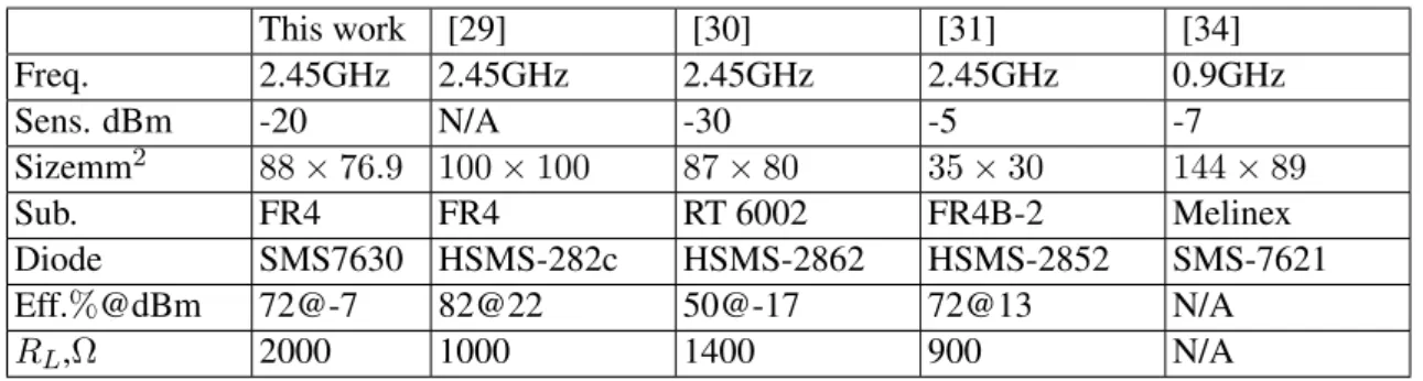
3.3 Comparison of our work with other rectenna in relevant literature. . . 30
3.4 Comparison of this study with the relevant research work in literatures. . . 37
4.1 Reactive Elements Values. . . 43
4.2 Comparison of this study with the relevant research work in literature. . . 46
5.1 Matching Component Values and its Part Number . . . 56
5.2 Spiral antenna parameters. . . 62
5.3 List of the DR-A and DR-B parameters. . . 67
5.4 Comparison of this study with the relevant research reported in the literature. . 70
6.1 Component values of the circuit architecture . . . 77
Chapter 1
Introduction
1.1 Background
Nowadays, the explosion growth in the electronic industry and the technology trend to de- sign and implement a much reduced footprint device has led engineers to devise a reliable and effective technique for energy power supply. Consequently, the energy harvesting was evolved as alternative method for the bulky batteries currently used in several electronic product in the market. The batteries not only is a bulk and hazard unit but it provides a hard and difficulties during maintenance and replacement. Therefore, the ability to wirelessly charge or entirely avoid the battery use is a future trend for engineer and research teams around the world.
Energy harvesting devices provide many benefits over conventional grid-powered and non- rechargeable battery-powered devices [1]. These advantages encompass energy self-sufficient, energy self-sustaining operation with lifetimes limited only by the lifetimes of their hardware.
These devices utilize the energy harvested from alternative natural resources such as solar, vib- erational, electromagnetic, thermoelectric, etc. As such, their widespread adoption will reduce the use of conventional energy and the accompanying carbon footprint, and benefit the environ- ment. In addition, these devices do not require conventional recharging, enabling untethered mobility, and deployment of these devices in hard-to-reach places such as remote rural areas, within structures, and within the human body. Wireless power transfer (WPT) has emerged
1.1 Background
Figure 1.1: Overview of the power densities from various energy sources and average power consumption of electronic devices and systems [2].
as one of the most promising solutions to achieve self-sustainable electronic device operation for Internet of Things (IoTs) applications. With the increasing number of pervasive and con- nected WSN together enhanced capacity for data management, it enables intelligent monitoring on many practical fronts such as environmental, and weather forecast. Rapid development of low-power wireless electronic systems has resulted in many research activities focused on the feasibility of a remote powering of these systems. Therefore, RF and microwave power transmission has become a focal point of interest for many years as a promising technique for powering electronic devices over distance. Harvesting tiny levels of ambient RF energy from various energy sources has been proven to be suitable for powering low energy devices and can extend the battery lifetime in such devices. Depending on the energy prerequisite of the device it is possible, in some cases, to constantly power the device so that the battery or energy storage unit never needs to be replace or charged via a cable. Although the RF energy is very low - RF power densities up to 300µW/cm2 have been measured - power density does vary by location. Overall, the energy that can be harvested with the ambient RF energy harvester has been validated as sufficient to eliminate the charge of an energy storage device.
1.2 Motivation
1.1.1 Ambient Energy Sources
Energy harvesting (EH) may be defined as the process of transforming ambient energy into electrical energy. Radiant (solar, infrared, radiofrequency), thermal, mechanical and biochem- ical are examples of the different forms of ambient energy. The energy harvesting efficiency can be defined as the ratio between the converted DC power and the available source of en- ergy. Among the different energy sources available around us, outdoor photovoltaic energy is the most powerful source of ambient energy, as shown in Fig. 1.1, but the conversion efficiency presents very low values of energy harvesting, (around 10%[3]). Moreover, the photovoltaic panels will only be able to provide this efficiency during a few hours per day depending on solar incidence. Thermoelectric energy harvesting needs a constant temperature gradient to achieve the peak of efficiency. For a temperature gradient of 10◦C, the efficiency would typically be 3%
and even for a 100◦C temperature gradient, an efficiency of 20%is expected [4]. Piezoelectric energy harvesting requires a specific and constant vibration frequency to have medium-high conversion efficiency [5]. Radio frequency (RF) energy harvesting requires sufficient levels of ambient RF energy density to be effective. In contrast to many other energy sources, RF signals are purposely generated and regulated. Due to the development of new radio technologies, the radio spectrum is becoming heavily populated: television, radio, cellular, GPS, WiFi, satellite and radar, among many others. Each of these frequency bands has an associated standard, which stipulates how it is used and the amount of RF authorised power to be transmitted. Depending on the location the RF power, energy densities can vary from 0.01µW/cm2to 100µW/cm2, and in some cases, where a dedicated RF transmitter is available, the RF power density can reach 300µW/cm2.
1.2 Motivation
Thanks to the progress in sensor technology, many low-power-consumption devices have been made available, enabling the possibility of powering the sensors using environmental ambient energy. An alternative energy harvesting approach is needed if ambient RF energy
1.3 Research Objective
harvesting is to be considered a widely applicable power source for the 26 billion Internet of Things (IoT) devices and the anticipated $300 billion industry being predicted by 20202. Pho- tovoltaic, thermoelectric, and piezoelectric energy harvesting systems have been developed as technologies that can power Low Energy Internet of Things devices (LE-IoT). These technolo- gies have their own inherent limitations, such as moving parts, fragility, and most importantly the constant presence of the energy source: solar energy harvesting only being available during daylight hours for example. Harvesting ambient RF energy, from WiFi, cellular networks and broadcast masts, offers an alternative solution to powering LE-IoT devices and could provide enough energy to extend the lifetime of these devices.
1.3 Research Objective
RF energy harvesting has been under development for many years but it has so far been limited in its application and commercial deployment. One of the main limiting factors has been the ability to design an RF energy-harvesting system that can operate at a high enough efficiency to harvest ambient RF energy from the very low power densities that are present in most city, home and office locations. As a result, current commercial systems require the use of a dedicated transmitter to boost RF power density levels to provide sufficient harvested power to undertake useful work.
RF energy is one example of the environmental free-energy. Multitude of radio devices are emitting electromagnetic energy into space and this energy is propagating every where and could be harvested using simple circuit called the rectenna, rectifying antenna. The rectennas are the most important elements in long-range wireless power transmission. The efficiency of rectenna mainly depends on their rectifiers. Therefore, to design a high-efficiency rectenna that guarantees the quality of a wireless power transmission system, more focus needs to be concen- trated on the investigation and design of rectifiers with reference to high RF-to-dc conversion efficiency. In rectifier circuits, the rectifying component is also the core element that determines the overall efficiency of the circuits and is normally realized with a diode or a transistor.
1.4 Contribution
In this dissertation, we focus on the energy harvesting technology using electromagnetic energy captured from multiple available ambient RF energy sources, such as TV and radio transmitters, mobile base stations, and microwave radios. This technique is very useful for sensors located in harsh environments or remote places, where other energy sources, such as wind or solar sources, are impracticable. In this context, this work presents an overview of advances achieved in RF harvesting field.
1.4 Contribution
Energy harvesting refers to the autonomously and simultaneously power feeding to multi- tude of sensors arranged in wide environment. Wireless power transfer tends to significantly attenuate once it transmitted from the power source. Consequently, the amount of power re- ceived at the far-field region is considered at the range of few micro watts. This puts constraint in the design of the receiver side, it should be more efficient, wide-bandwidth, compact, and simple design.
In this regard, the objective of this work is to design and implement a high-efficient energy harvesting system that meets the prescribed criteria. Several approaches have been proposed for the design of a high-efficient single band rectifiers. Indeed these rectifiers were combined with an antenna to realize the energy harvesting power feeding unit. Indeed a wide-band, simple, and optimum operated rectifier was developed to harvest power from across broadband spectrum ranging from the current broadcasting service bands, cellular bands, and the ISM 2.4 GHz and 900 MHz frequency allocated spectrum. Moreover, a balanced-output differential rectifier configuration was suggested to obtain a direct feeding connection to the electronic devices. The differential rectifier provides an output voltage that could be directly used for the transistor biasing as it needs +/- DC voltage. To achieve the system verification, the proposed prototypes were integrated with a real-applications, and it was tested for continuous operation over long time period.
To summarize, the developed rectifier architectures offer an important progress in the current
1.5 Thesis Organization
research belonging to the RF energy harvesting technology. The outcomes of this research can be considered among the latest advancement of the wireless power transfer research area.
This research has came up with more than five international journal articles as well as many national/international conference papers.
1.5 Thesis Organization
In this study, we introduce an investigation of the recent advancement in the RF energy har- vesting techniques. Besides, we developed a new rectifier circuit topologies for improving the overall conversion efficiency, minimize the circuit footprint, maximize the circuit performance, deploy with a real application like WSN, and simple circuit design technique so facilitate pro- cedures of the circuit implementation. These features offer a great advantages to the proposed design. The rest of the thesis is arranged according to the following order:-
• The different rectifier circuit configurations either based on the CMOS or the Schottky diode are discussed in chapter 2. Both the analysis and characterization of each circuit are conducted and a full comparison is made between them to get out the most efficient circuit. Moreover, it summarizes various concepts and equations that are particularly use- ful in the analysis of the energy harvesting circuit structures. In addition, the impedance matching network design procedures are described and the different mathematical analy- sis is conducted in this chapter.
• After analyzing the performance of the different rectifier architecture, an energy harvest- ing circuit based on the Schottky diode elements operating at 2.45 GHz is designed, eval- uated, and characterized. In chapter 3, a single band rectifier is illustrated.
• Broadband rectifiers are essential to extend the efficient operating response over a wide frequency band. A compact and 1.5 Octave bandwidth rectifier is demonstrated in chapter 4.
1.6 Conclusion
the majority of power supply circuit should be followed by a conditioning circuit that convert from an unbalanced DC voltage to a balanced form. This will add a circuit com- plexity and increased large size. To eliminate such issue, we developed a a differential energy harvesting circuit that could provide the power directly to the electronic devices without the need for any conditioning circuit. The design of differential rectifier is intro- duced in chapter 5.
• A rectifier circuit based on 180nm CMOS technology is explained in chapter 6. The proposed circuit is designed and tested at operating frequency 2.45 GHz.
• A real application for the different proposed energy harvesting circuits is demonstrated in chapter 7. The deployment of an energy harvesting circuit is achieved with a Blue- tooth low energy unit (BLE) which is attached with multitude of environmental sensors to measure vaiouse physical phenomenon.
• A future plan is considered in chapter 8. The theme of the forthcoming research work will further improve the harvesting circuits to maximize the efficiency for the micro-power input levels.
1.6 Conclusion
This chapter presented an introduction about the energy harvesting technology. Moreover, it indicated the purpose, and motivation of the current dissertation by demonstrating the objectives of each chapter.
Chapter 2
Different Rectifier Architectures
Recently, there has been an interest of research interests in radio frequency (RF) energy harvesting/scavenging technique, or RF harvesting in short, which is the capability of convert- ing the received RF signals into electricity. This technique becomes a promising solution to power energy-constrained wireless networks. Conventionally, the energy-constrained wireless networks, such as wireless sensor networks, have a limited lifetime which largely confines the network performance. In contrast, an RF energy harvesting network (RF-EHN) has a sustain- able power supply from a radio environment. Therefore, the RF energy harvesting capability al- lows the wireless devices to harvest energy from RF signals for their information processing and transmission. Consequently, RF-EHNs have found their applications quickly in various forms, such as wireless sensor networks, wireless body networks, and wireless charging systems. In RF energy harvesting, radio signals with frequency range from 300GHz to as low as 3kHz are used as a medium to carry energy in a form of electromagnetic radiation. RF energy transfer and harvesting is one of the wireless energy transfer techniques. The other techniques are inductive coupling and magnetic resonance coupling. Inductive coupling is based on magnetic coupling that delivers electrical energy between two coils tuned to resonate at the same frequency. The electric power is carried through the magnetic field between two coils. Magnetic resonance cou- pling utilizes evanescent-wave coupling to generate and transfer electrical energy between two resonators. The resonator is formed by adding a capacitance on an induction coil. Both of the
2.1 Rectifier configurations
above two techniques are near-field wireless transmission featured with high power density and conversion efficiency. The power transmission efficiency depends on the coupling coefficient, which depends on the distance between two coils/resonators. The power strength is attenuated according to the cube of the reciprocal of the distance, specifically, 60 dB per decade of the distance, which results in limited power transfer distance. Besides, both inductive coupling and resonance coupling require calibration and alignment of coils/resonators at transmitters and receivers. Therefore, they are not suitable for mobile and remote replenishment/charging. In contrast, RF energy transfer has no such limitation. As the radiative electromagnetic wave can- not retroact upon the antenna that generated it (by capacitive or inductive coupling) at a distance of aboveλ/(2π) , RF energy transfer can be regarded as a far-field energy transfer technique.
Thus, RF energy transfer is suitable for powering a larger number of devices distributed in a wide area. The signal strength of far-field RF transmission is attenuated according to the re- ciprocal of the distance between transmitter and receiver, specifically, 20 dB per decade of the distance.
2.1 Rectifier configurations
RF energy extracted from free space usually possesses low power density since the electric field power density decreases at the rate of1/d2, where d is the distance from the RF source [6].
Therefore, a power amplifier circuit is required that yields enough DC energy from the electro- magnetic waves to drive the loads. This gives rise to two possibilities, if the power consumption of the load is lower than the average power harvesting, the electronic devices at the load may work continuously; otherwise, if the load consumes more energy than the power harvesting circuit can generate, the devices cannot work continuously [7]. Rectifying is the most popular application of diodes, which refers to the conversion of AC current to DC current. In terms of power harvesting application, the RF signal retrieved in the antenna has a sinusoidal waveform.
The signal after transformation through impedance matching network(IMN) would be rectified and boosted to meet the power requirements of the application. The most fundamental topology
2.1 Rectifier configurations
Figure 2.1:Some common topologies of a rectifier [8].
of the rectifier is the half-wave rectifier that comprises of a single diode D1 (Fig. 2.1(a)). When AC voltage transfers through D1, only the positive cycle remains and the negative cycle is cut- off; thus, it diminishes half of the AC power. Moreover, the outputVout is discontinuous since the negative cycle is cutoff. Despite its simplicity, a half-wave rectifier is usually inadequate for common applications. Hence, a full-wave rectifier is more preferable. The circuit design of the full-wave rectifier is shown in Fig. 2.1(b). During the first negative cycle of AC input, diode D1 is conductive and capacitor C1 is charged to the corresponding energy level ofVpeakof the input.
Then, at the next positive cycle, diode D1 is blocked, diode D2 is conductive so that capacitor C2 is also charged. In consequence, the output Vout would see two capacitors in series (each one is storing a voltage of Vpeak). Thus, Vout is twice Vpeak. Therefore, this topology is more stable and efficient than the half-wave rectifier. There is also a bridge rectifier that rectifies both positive and negative cycles of the AC input but retainsVout = Vpeak by alternatively blocking pairs of diodes D1, D4 and D2, D3 (Fig. 2.1(c)).
Voltage multiplier is a special type of rectifier circuit that converts and boosts AC input to DC output. In some case where the rectified power is inadequate for the application, there is
2.1 Rectifier configurations
Figure 2.2:Common voltage multiplier configurations: (a) Three stages CockcroftWalton voltage multiplier, (b) Four stages Dickson voltage multiplier, (c) Four stage Dickson voltage multiplier using CMOS technology, (d) Two stages voltage multiplier comprised of differential drive unit [8].
a need for boosting the output DC by stacking single rectifiers into series, forming the voltage multiplier [9]. Several configurations of the voltage multiplier are shown in Fig. 2.2. The most fundamental configuration is the CockcroftWalton voltage multiplier (Fig. 2.2(a)). This circuits operational principle is similar to the full-wave rectifier (Fig. 2.1(b)) but has more stages for higher voltage gain. The Dickson multiplier in Fig. 2.2(b) is a modification of CockcroftWal- tons configuration with stage capacitors being shunted to reduce parasitic effects. Thus, the Dickson multiplier is preferable for small voltage applications. However, it is challenging to obtain high power conversion efficiency (PCE) due to the high threshold voltage among diodes creating leakage current, thus reducing the overall efficiency. Additionally, for high resistance loads, output voltage drops drastically leading to low current supply to the load. The MOSFET (metal oxide semiconductor field effect transistor) technology is overcoming the limitations of diodes and becoming an alternate solution for rectifying and boosting. Owing to MOSFET
2.2 Impedance Matching Network
technology, Dickson multiplier can be integrated together in integrate circuits (IC) by replac- ing diodes with NMOS as shown in Fig. 2.2(c). Relatively low threshold voltages and high PCEs are features of this design. Moreover, differential drive voltage multiplier (Fig. 2.2(d)) is widely used because of its low leakage current and potential for further modification for spe- cific applications. A detail explanation and analysis is presented in [10, 11]. As the number of stages getting increase, there is more loss across each added stage. However, the tradeoff is higher voltage multiplication and small threshold voltage at the first stage. On the other hand, a voltage multiplier with a few stages has less voltage drop between its stages but requires higher threshold voltage for all stages to work simultaneously. For this reason, a voltage multiplier becomes more sensitive when a large number of stages are present and becomes more efficient at fewer stages. This tradeoff feature was analyzed in several researches [12,14]. Therefore, the optimal number of stages should be considered depending upon the application targets.
2.2 Impedance Matching Network
IMN is a critical circuit design for an efficient rectifer. To ensure maximum power transfer between the signal source and the terminal load, an IMN should be introduced between it. Bode [15] first showed what the physical limitations were on the broadband impedance matching of loads consisting of a reactive element and a resistor in either series or parallel configuration.
Later, Fano [16] presented the general limitations on the impedance matching of any load.
Fano’s work show the efficiency of transmission and bandwidth are exchangeable quantities in the impedance matching of any load having a reactive component.
To illustrate the theoretical limitations which exist on broadband impedance matching, con- sider the example shown in Fig. 2.3 where the load to be matched consists of a parallel RC connection capacitor C1 and resistor Ro. A lossless impedance-matching network is inserted between the generator and the load, and the input reflection coefficient between the generator
2.2 Impedance Matching Network
Figure 2.3:Example of an impedance matching problem.
and the impedance matching network is given by 2.1.
Γ = Zin−Rg
Zin+Rg (2.1)
The work of Bode-Fano shows that there is a physical limitation on whatΓcan be as a function of frequency. The best possible results are limited as indicated by the following relation:-
Z ∞
0
ln| 1
Γ |dw= π
RoC1 (2.2)
Recall that for a passive circuit0 ≤| Γ |≤ 0, for total reflection| Γ |= 1, and that for perfect transmission | Γ |= 0. Thus, the larger ln | 1/Γ | is the better the tranmssion will be. But Equation 2.2 indicates that the area under the curve ofln | 1/Γ | vswcan be no greater than π/RoC1.
If a good impedance match is desired fromwatowb, best results can be obtained if|Γ|= 1 at all frequencies except in the band fromwatowb. Thenln|1/Γ|= 0at all frequencies except in thewa towb band, and the available area under theln| 1/Γ |curve can all be concentrated in the region where it does the most good. With this specification, Equation 2.2 becomes:-
Z wb
wa
ln| 1
Γ |dw= π
RoC1 (2.3)
| | | |
2.2 Impedance Matching Network
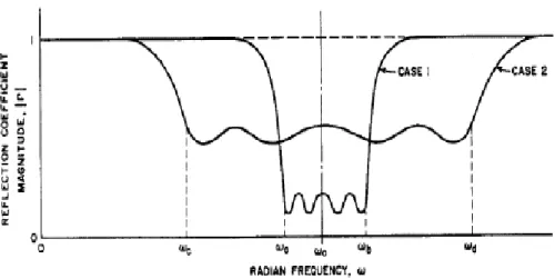
Figure 2.4: Curves illustrating relation between bandwidth and degree of the impedance match possible for a given load having a reactive component. [17]
frequency becomes
Γ = exp[−π/(wb−wa)RoC1] for wa≤w≤wb (2.4) Γ = 1 for 0≤w≤wa and wb ≤w≤ ∞ (2.5) Equation 2.5 says that an ideal impedance-matching network for the load in Fig. 2.4 would be a band-pass filter structure which would cut off sharply at the edges of the band of impedance match. The curves in Fig. 2.4 show how|Γ | vs wcurve for practical band-pass impedance matching filters might look.The curve marked Case 1 is for the impedance matching of a given load over the relatively narrow band fromwa towb, while the curve marked Case 2 is for the impedance matching of the same load over a wider band fromwctowcusing the same number of elements in the impedance matching network. The rectangular|Γ |characteristic indicated by Equation 2.5 is that which would be achieved by an optimum band-pass matching filter with an infinite number of elements.
2.3 Chapter Summary
2.3 Chapter Summary
In this chapter, different rectifier architectures were extensively discussed. Each architecture was introduced and compared for the desired performance. The maximum power transfer be- tween the source and a load terminal is achieved using an impedance matching network so the impedance matching network investigation was considered in the chapter. Moreover, a compar- ative study was made between the CMOS and Schottky diode as rectifier.
Chapter 3
2.45 GHz Single Band RF Rectifier
3.1 Introduction
This chapter looks into the underlying RF energy harvesting issues at low input ambient power levels below 0 dBm where efficiency degradation is severe. The chapter illustrate two different design for improving the conversion efficiency.
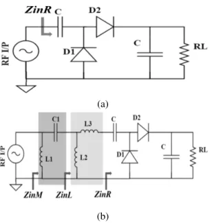
The first design aims to improve the rectenna sensitivity, efficiency, and output DC power.
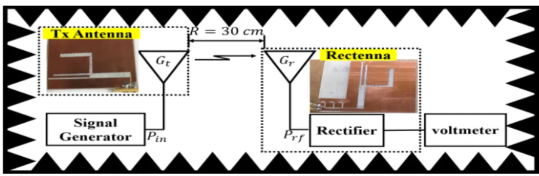
In the same manner, we are using a straightforward and compact size rectenna design. The receiving antenna is a coplanar waveguide (CPW) slot monopole antenna with harmonic sup- pression property and a peak measured gain of 3 dBi. Also, an improved antenna radiation characteristics, e.g radiation pattern and gain covering the desired operating band (ISM 2.45 GHz), is observed. The rectifier is a voltage doubler circuit based on microstrip (MS) structure.
Two architectures of rectenna were carefully designed, fabricated and tested. The first layout;
antenna, and rectifier were fabricated separately and then connected using a connector. The peak efficiency (40%at−5dBm) achieved is lower than expected. To improve the efficiency, a high compactness and simple integration between antenna and rectifier are achieved by using a smooth CPW-MS transition. This design shows improved conversion efficiency measure- ment results which typically agree with the simulation results. The measured peak conversion efficiency is 72% at RF power level of -7 dBm and a load resistance of 2 kΩ.
3.2 Literature Review
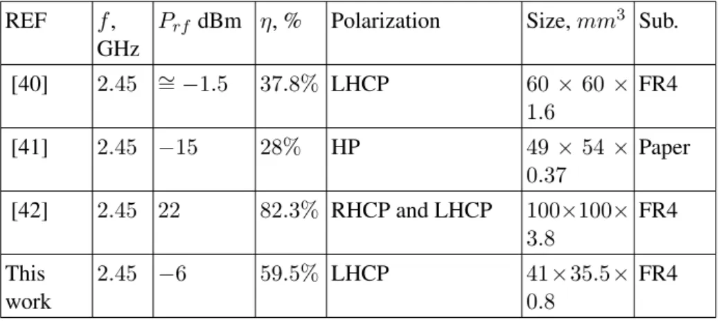
The second design presents the implementation of a compact, reliable, effective, and flexible energy harvesting (EH) rectenna design. It integrates a simple rectifier circuit with a circularly polarized one-sided slot dipole antenna around 2.45 GHz ISM frequency band for wireless charging operation at low incident power densities, from 1 to 95µW/cm2. The rectenna struc- ture is printed on a single layer, low cost, commercial FR4 substrate. The integration of the rec- tifier and antenna produces a low-profile and high performance circularly polarized rectenna. In order to maximize the system efficiency, the matching circuit introduced between the rectifier and antenna is optimized for a minimum number of discrete components and it is constructed using multiple of L-slot defects in the ground plane. For a given input power of −6 dBm intercepted by the circularly polarized antenna with 3 dBi gain, the peak RF-DC conversion efficiency is 59.5%. The rectenna dimensions are41×35.5mm2. It is demonstrated that the output power from the proposed rectenna is higher than the other published designs with a sim- ilar antenna size under the same ambient condition. Thanks to its compact size, the proposed rectenna could found a range of potential applications for wireless energy charging.
3.2 Literature Review
Recently, many rectennas have been reported, including a rectenna using a reconfigurable patch resonator [25, 26], a multiband frequency rectenna [27, 28], and rectenna with various patch antenna configurations [29]Normally, the DC conversion efficiency, minimum detectable RF input power, and loading effect become one of the important considerations for rectenna designs. Most of the implemented rectennas are based on deploying either MS line or CPW design. For our best of knowledge, no rectenna combine both formats has been reported. The most recent advancement in RF EH is discussed in next sections.
In [32], authors propose an energy-harvesting IC fabricated in 0.25µm CMOS that can charge a 3.3 V lithium battery with a delivered power ranging 0.5−5 mW utilizing up to four different energy sources have simultaneously efficiency up to 73.3%. A 900 MHz RF energy harvesting system is proposed for a far-field wireless power transfer application in [33]. Two
3.2 Literature Review
tuning techniques are employed and the power conversion efficiency is higher than 30%over an input power range -10 to 12 dBm with a peak value of 47%at 0 dBm for a 1.5 V output voltage.
The maximum output voltage of the system is 2.45V with a sensitivity of -15 dBm. The design of a flexible hybrid printed low-cost RF energy harvester has been demonstrated in [34]. The performance of the designed far-field RF energy harvester has been verified through wireless experiments demonstrating output voltages above 2.9 V for input power levels above 0 dBm from 0.8 GHz∼l.l5 GHz. Authors in [35] introduces a wireless receiver system operating at 900 MHz band and fabricated in CMOS 180 nm, the proposed RF receiver system architecture can operate at the presence of unavoidable high out-of-band blockers (0 dBm) yet consumes 534 µW. Moreover, 46% of this dc power is extracted from existing blockers via RF energy harvesting techniques. Although the previous studies offered numerous benefits to the energy harvesting technology, it still suffers from several practical issues like high fabrication cost, large size, power consumption,..etc.
The interfacing techniques between CPW and MS structures is realized using either electri- cal contact or electromagnetic (EM) coupling [36]Although the surface-to-surface EM coupling techniques offer advantages like via-free structure and low-loss, it suffers from design complex- ity, narrow bandwidth, and large size.
In this study, the electrical connection is selected for the interconnection between CPW and MS structure. Electrical connection provides broadband operation and compact size. It could be realized using via holes, bonding wires, or abrupt steps in the conductor. For the proper connection between CPW and MS structures, a via interconnection is selected. The placement of these vias is critical to achieving the desired impedance and low loss characteristics through parasitic wave modes suppression.
Diode nonlinearities may result in some high-order harmonics that may be radiated by the antenna. Serious nonlinearities noticed at the second (2nd), and third (3rd) harmonics almost have an adverse effect on the rectifier efficiency. Therefore, the proposed slot antenna has notched bands for the 2nd, and 3rd harmonics suppression of the fundamental frequency of 2.45 GHz.
3.3 Antenna-Rectifier Direct Connection
Figure 3.1:Photograph of the fabricated antenna with the structure parameters are given on the layout.
3.3 Antenna-Rectifier Direct Connection
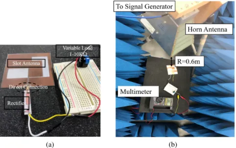
We started our discussions by describing the designs of CPW slot antenna and the rectifying circuit. They are fabricated separately and assembled using micro-miniature coaxial (MMCX) connectors. This configuration represents the direct connection of Case 1 which will be dis- cussed in Sec. 3.5.1.
3.3.1 CPW Slot Antenna
Slot antenna is a good candidate for energy harvesting applications owing to its wide impedance bandwidth, simple structure, low profile, and easy fabrication. Slot antennas can have a rela- tively large impedance bandwidth, especially antenna with a wide slot. The proposed antenna geometry along with the fabricated antenna photograph is illustrate in Fig. 3.1; the antenna is printed on single metal FR4 substrate of thickness 0.8 mm (h) and relative permittivity 4.4 (r). The antenna structure consists of L-section (constituted byLp ×Wp andLm×Wm) and rectangular slot (constituted by Ls×Ws). It is fed by 50Ω CPW transmission line having a metal strip of width Wf, and coupling gap distance of g. The total dimensions of the antenna
3.3 Antenna-Rectifier Direct Connection
Table 3.1:Parameters’ values of the antenna design.
lp wp lm wm ws ls wf lf g
10 23 39 13 32 21 1.15 18 0.3
All units are given in mm.
are 78×76.9×0.8 mm3. The fabricated prototype of the CPW slot antenna mounted with an MMCX female connector is shown in Fig. 3.1(b). The approximate resonant frequency can be estimated by the slightly modified equations 3.1 [37]:
fr = 300 (ls+ws)×√
ef f, ef f = 2×r
1 +r (3.1)
In the empirical formula, fr is the resonant frequency of the fundamental mode in GHz,ls andwsare the inner width and length of the rectangular slot, respectively in millimeters andef f
is the effective dielectric constant. To achieve the desired broadband impedance bandwidth and harmonics suppression, a rectangular slot and L-slot are used respectively. The bandwidth of the asymmetrical slot antenna can be obtained with a proper impedance matching andV SW R <2 by changing the antenna design parameters. A commercially available simulation software HFSS was used for the electromagnetic and numerical analysis simulations of the antenna.
A parametric study of the rectangular slot and L-section dimensions is carried out in order to obtain an efficient excitation and good impedance matching over the desired frequency band.
To accurately determine the influence of these parameters, only one parameter is varied at a time while others are kept constant. The antenna return loss dependent on the rectangular slot and L-section slot dimensions is shown in Fig. 3.2.
As the rectangular slot width (Ws) increases, the response (return loss) moves toward low- frequency region. Changes in L-slot dimensions (Wm) affect the 2nd and 3rd harmonic compo- nents. The L-slot notched on the antenna structure provides a suppression feature of 2nd and 3rd harmonics (4.9 GHz and 7.35 GHz respectively). Therefore, the effect of spurious resonance is minimized.
It is noted that the input impedance of the antenna at the fundamental frequency 2.45 GHz,
3.3 Antenna-Rectifier Direct Connection
Figure 3.2:Parametric study of antenna dimensions, Return lossS11
(a) (b)
(c) (d)
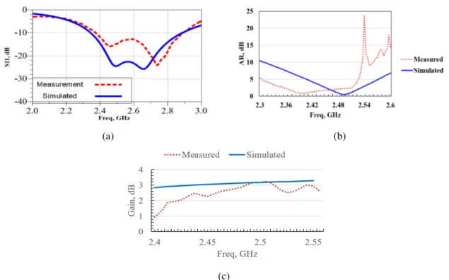
Figure 3.3: Comparison between the antenna experimental and simulation results (a) Return loss S11 over a wideband (1-8 GHz) to account for the 2nd and 3rd harmonics, (b) Return lossS11over the band of interest, (c) Realized gain, (d) Normalized radiation pattern (XZ plane).
3.3 Antenna-Rectifier Direct Connection
second harmonic frequency 4.9 GHz, and the third harmonic frequency 7.35 GHz are 39-j2.98 Ω, 131-j49 Ω, and 30+j47 Ω, receptively. Thus, the desired antenna performance has been achieved. After completing a thorough parametric study on the antenna geometry, the optimum design parameters of the antenna are set and summarized in Table 3.4.
Antenna measurements were carried out in an anechoic chamber. From the measured result in Fig. 3.3, it is observed that both measured and simulated return losses (Fig. 3.3(a)) are coinciding well around the fundamental resonant frequency 2.45 GHz, but it is slightly shifted at the higher frequencies above 5.2 GHz. Furthermore, the antenna is found to be matched to the input port of rectifier at 2.45 GHz and mismatched at high-order harmonics. The measured actual antenna gain is reasonable agreeing with the simulated gain as shown in Fig. 3.3(c). The measured gain is varying between a peak value of 3.2 dB and minimum 2.2 dB in the frequency range from 2 to 3 GHz . The normalized radiation pattern of the proposed antenna was measured at frequency 2.45 GHz, the measured far-field and simulated results are plotted in Fig. 3.3(d).
As illustrated in the figure, the asymmetrical slot antenna produces the main lobe radiations in both the forward (+z) and backward direction (-z). Therefore it is considered as a bidirectional antenna with the side lobes entirely attenuated. The measured results are found to agree well with the simulated ones.
3.3.2 Rectifier Circuit Design
Radio frequency signal captured by the antenna is an alternating current (AC) signal. In order to convert AC signal to DC signal, a rectifier circuit is used. The most popular rectifier used is Greinacher circuit or voltage doubler [38]. The topology of this circuit (described in Fig. 3.4) is typically used for most of the reported rectenna, but the selection of transmission line model is different from one design to another. MS transmission lines are selected for the rectifier design due to its simple design, low cost, and low loss at moderately high frequencies.
The 50Ωimpedance matching is depending on the values of the L-matching circuit parameters L, C and the width of impedance transformer. Values of L and C are chosen as 5.6 nH and 1 pF, respectively. The width of theλ/4impedance transformer is selected to be 7 mm. The rectifier
3.3 Antenna-Rectifier Direct Connection
Figure 3.4:The layout of the MS rectifier circuit.
(a) (b)
Figure 3.5:The analysis of the rectifier circuit performance (a) Return lossS11, (b) Efficiency versus input signal frequency atPin=-20 dBm, (b) Efficiency versus input signal power
circuit is printed on a two side FR4 substrate of thickness 0.8 mm (h) and relative permittivity 4.4 (r). The simulations were carried out using schematic, momentum and co-simulation tools of ADS Keysight Tech.
The most important figure of merit of a rectifier is the efficiency. RF-DC conversion effi- ciency is given by: -
η(%) = PDC
PRF = Vout2
RL×PRF (3.2)
wherePDC is the output DC power,RL is the resistive load,Vout is the output DC voltage, andPRF is the RF received power. As shown in Fig. 3.5(a, b), the rectifier return loss is properly matched at the desired frequency so that a significant increasing of the efficiency has achieved as well. Both the simulated and measured results of rectifier efficiency are shown with the variation of Pin as depicted in Fig. 3.5(b). However the simulated maximum efficiency of72%
3.4 Rectenna Integration
was obtained at RF input power of−11dBm and load resistance 2 kΩ, the measured efficiency is25%only at the same constraints. The maximum measured efficiency 33%was achieved at
−5 dBm. To account for the fabrication losses, series resistive element of 2 Ω is connected in replace of the soldering pads, afterwards the simulation conducted again. This shows that measurement and the parasitic simulated results are slightly matched.
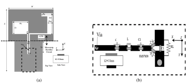
3.4 Rectenna Integration
The simplest way to connect the CPW slot antenna with the MS rectifier circuit is using an MMCX connector which will be introduced in Sec. 3.5.1. The main disadvantages of this ap- proach are that it couldn’t be integrated with the applications based on wireless power transfer, and it contributes to the ohmic losses of the system caused by MMCX connector. Consequently, a novel CPW-MS smooth transition is presented for improving the conversion efficiency, and reducing the size of the proposed rectenna. This configuration represents the second rectenna design architecture (Case 2 in Sec. 3.5.2). For any transmission line with discontinuities caused by impedance transitions [39], these will result in: -
• Some amount of energy reflected back to the source at the point of impedance transition.
For example, the transition of the RF energy from the connector to the PCB often causes reflections.
• When the energy of the RF signal has two different modes of transitions, reactance is created. Parasitic reactance will contribute to the detuning of the desired design frequency.
Based on the aforementioned reasons, particular design procedures must be followed to con- struct a smooth transition between a CPW and MS structures. Such transition is implemented using a single via electrically connected between the CPW antenna feedline and MS feed point.
Moreover, the ground of CPW slot antenna could be used as the ground for MS. In order to keep similar antenna performance as discussed in Section (2.1). The same asymmetrical slot antenna is used with minor changes, but the rectifier circuit configuration is developed. The antenna
3.4 Rectenna Integration
(a) (b)
Figure 3.6: Case 2 antenna layout and the corresponding rectifier circuit (a) Case 2 antenna layout, (b) Case 2 rectifier layout mounted on the backside of (a) in the area specified by the dashed line.
ground plane is extended to cover the rectifier circuit dimensions. The antenna feed-line is in- creased to lengthLt, and at the end of the feed-line, a via is inserted for linking the input of the rectifier circuit to the antenna as illustrated in Fig. 3.6(a). After precise optimization (using the HFSS electromagnetic software) of the transition structure dimensions (Lt,Gt, and the position of the via along the feed line), the correct values were obtained. The length is selected asLt= 5mm and the gap to the planar groundGt=0.5 mm.
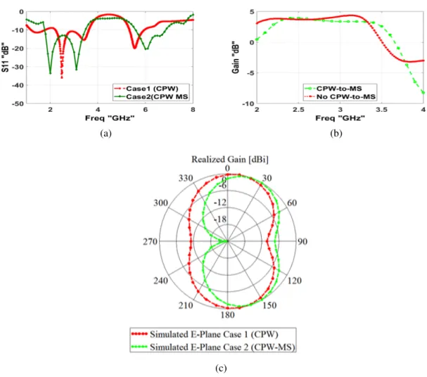
To validate the design of CPW-MS transition, the antenna response of Case 2 was compared to that of Case 1. In Fig. 3.7(a), the return loss for both cases (Case 1, i.e. CPW slot antenna with no transition, and Case 2, i.e. CPW slot antenna with CPW-MS transition) are given.
It is observed that the S11 curve of the proposed designs is in good agreement. In this way, broadband impedance matching over the desired frequency range and the harmonic suppression property without any changes at 2nd and 3rd harmonics characteristics are maintained. Also, gain comparison of Case 1 and Case 2 is presented in Fig. 3.7(b). As expected, the gain of both cases approximately is in agreement over the desired bandwidth. The radiation pattern characteristics are quite different from the previous case as shown in Fig. 3.7(c). This is due to the presence of a ground plane behind the antenna feed. This metal sheet acts as a reflector, so
3.4 Rectenna Integration
(a) (b)
(c)
Figure 3.7: Comparison between the simulated results of Case 1 and Case 2 antenna response (a) Return loss S11, (b) Realized gain, (c) Normalized radiation pattern (XZ Plane).
most of the radiations are reflected back in the opposite direction.
On the other hand, the rectifier circuit is developed, instead of using 0.8 mm double side substrate, the rectifier circuit is fabricated separately on the bottom side of a 0.8 mm double layer FR4 substrate as depicted in Fig. 3.6 (b). Then, a via hole is drilled for connecting the antenna feed to the input of the rectifier circuit. This will be discussed clearly in the next section.
Since the the rectifier circuit substrate configuration has slightly changed, the input impedance has to be optimized for maximum power transfer. The co-simulation between antenna and rectifier was done by exporting Z-parameter file of the antenna with CPW-MS transition from
3.4 Rectenna Integration
(a) (b)
Figure 3.8:The connection and measurements of case 1 rectenna (a) antenna-rectifier interfacing, (b) Photograph of the measurement setup.
Figure 3.9:Case 2 antenna-rectifier integration .
HFSS and importing it into ADS software as input impedance of the rectifier circuit power source. This was done to ensure the optimum matching between the CPW-MS antenna and the rectifier. In this case, the impedance transformer is removed because the resistive part of input impedance of rectifier (40-j8Ω) is almost identical to that of the antenna (38+j11Ω). Thus the circuit dimensions are shrinking down. The imaginary part of the slot antenna (capacitive) is compensated by changing the LC series components. Therefore, only the value of inductance L has changed to 8.2 nH and C is kept constant.
![Figure 1.1: Overview of the power densities from various energy sources and average power consumption of electronic devices and systems [2].](https://thumb-ap.123doks.com/thumbv2/123deta/9840063.1895446/19.892.216.755.246.496/figure-overview-densities-various-sources-average-consumption-electronic.webp)