A Study on Energy-and-Area-Efficient Charge Redistribution Successive Approximation
Analog-to-Digital Converters
August 2010
CHEN, Yanfei
Abstract
In battery-powered mixed-signal applications including data communication and image processing systems, high performance analog-to-digital converters (ADC) are in great demand. This work aims to design medium resolution and moderate sampling rate ADCs with very low power consumption and small footprint.
Energy and area savings are realized in several aspects. In architecture selection, charge redistribution based successive-approximation-register (SAR) architecture shows the highest power efficiency, benefiting from the structure containing only one active analog component. In circuit design, each of ADC building blocks is simplified and optimized to reduce power consumption and area. Split capacitor digital-to-analog converter (CDAC) is used to reduce input load capacitance and area. This work proposes a split CDAC calibration scheme to improve linearity performance. A bridge capacitor larger than conventional design is implemented so that a tunable capacitor can be added in parallel with the lower-weight capacitor array to compensate for mismatches. A tri-level charge redistribution scheme is proposed to reduce the CDAC switching energy and improve the settling speed. Differential capacitor bottom-plate charge-sharing technique is used to realize the third reference level without consuming extra power. The tri-level scheme also helps simplifying the SAR control logic circuits by eliminating the need for set-and-reset function. To avoid on-chip reference generation and therefore save power and cost, any reference voltage different from the supply voltage is removed.
Asynchronous processing technique is used to eliminate power-hungry GHz clock generation and speed up the SAR algorithm as well.
The thesis is organized as follows:
Chapter 1 is an introduction of the overall study, starting from the data converter history and a variety of architectures. The trend in ADC design and the motivation of this research is summarized.
Chapter 2 presents the split CDAC calibration scheme. The issues of conventional split CDACs are analyzed, followed by the principle and implementation of the proposed calibration method. The feasibility is proved by the test chip measurement results.
Chapter 3 presents the tri-level charge redistribution scheme. The switching energy inefficiency and settling problem of the conventional method are first analyzed. Then the tri-level method and differential capacitor bottom-plate charge-sharing technique are introduced in details. The improvement of energy efficiency and settling speed are shown in simulation results.
Chapter 4 gives a high performance SAR ADC design, which combined the split CDAC calibration and the tri-level charge redistribution techniques. Circuit design details of each building block are provided. The ADC test chip implemented in a stand CMOS process is measured and compared with other state-of-the-art converters.
Chapter 5 summarizes the thesis and provides a prospect of future work.
Contents
Abstract... i
Contents ... iii
List of Tables... v
List of Figures... vi
Chapter 1 Introduction ... 1
1.1 Background... 2
1.2 Research Motivation... 16
1.3 Dissertation Organization... 20
References... 22
Chapter 2 Split Capacitor DAC Calibration ... 25
2.1 Charge Redistribution SAR ADC ... 26
2.2 Split Capacitor DAC... 28
2.3 Split CDAC Calibration ... 33
References... 50
Chapter 3 Tri-Level Charge Redistribution ... 52
3.1 Background... 53
3.2 Tri-Level Charge Redistribution... 58
References... 68
Chapter 4 9-Bit 100-MS/s ADC Design... 70
4.1 ADC Architecture ... 71
4.2 DAC Design... 73
4.3 Comparator Design... 78
4.4 SAR Control Logic Design... 80
4.5 Measurement Results... 82
References... 96
Chapter 5 Summary ... 98
5.1 Dissertation Summary... 99
5.2 Future Work...101
References...104
Acknowledgements...105
List of Tables
Table 1.1 ADC Architecture Timeline Table 2.1 Comparison with Published Work Table 4.1 Performance Summary
Table 4.2 Comparison with Published Work
List of Figures
Figure 1.1 3-bit Flash ADC
Figure 1.2 N-bit Two-Stage Subranging ADC
Figure 1.3 Basic Pipelined ADC with Identical Stages Figure 1.4 Basic Successive Approximation ADC Figure 1.5 Successive Approximation ADC Algorithm Figure 1.6 Single and Multi-bit Sigma-Delta ADC Figure 1.7 ADC Applications
Figure 1.8 ADC Architectures Domain Area
Figure 1.9 Trend of ADC Performance in the Past Decade
Figure 1.10 Target ADC Performance (a) Energy Efficiency vs. Sampling Rate (b) Die Area vs. ENOB Figure 1.11 Dissertation Organization
Figure 2.1 Charge Redistribution SAR ADC
Figure 2.2 8-Bit CDACs (a) Binary-Weighted Array (b) Split Array with Fractional Bridge Capacitor (c) Split Array with Unit Bridge Capacitor (d) Split Array with Two Unit Bridge Capacitor Figure 2.3 ADC Code Transitions with Nonlinearity
Figure 2.4 ADC Code Transition with Gain Error
Figure 2.5 Split Capacitor Array with Mismatch Calibration Figure 2.6 Equivalent Circuits of the L-side Capacitor Array
Figure 2.7 Split CDAC Calibration Implementation with Timing Diagram Figure 2.8 Implementation of CC
Figure 2.9 Comparator with Two-Step Digital Timing Control Charge Compensation Offset Calibration Figure 2.10 Simulated Relationship between Offset and Delay Time td
Figure 2.11 Chip Micrograph
Figure 2.12 ADC Histogram Test Setup.
Figure 2.13 Sine-wave Probability Density Function Figure 2.14 Measured DNL and INL Before Calibration Figure 2.15 Measured DNL and INL After Calibration Figure 3.1 2-Bit Conventional Charge Redistribution ADC
Figure 3.2 MSB Settling of DAC Output with Switch Driving Mismatches
Figure 3.3 Down Transition Settling of DAC Output with Switch Driving Mismatches Figure 3.4 Proposed Tri-Level Charge Redistribution DAC
Figure 3.5 Extra Bit Resolution in The Tri-Level DAC Figure 3.6 Differential Tri-Level Charge Redistribution DAC Figure 3.7 Switching Energy versus Output Code
Figure 3.8 Simulated Output Settling of the Conventional and Proposed DAC with Switch Driving Mismatches (a) MSB Settling (b) Down-Transition Settling.
Figure 4.1 ADC Architecture with Timing Diagram
Figure 4.2 Implementation of the Tri-Level Split Capacitor DAC with Mismatch Calibration Figure 4.3 Largest Voltage Swing in Floating Nodes (a) Node P (b) Node Q
Figure 4.4 Output Settling of the MSB vs. Input Signal
Figure 4.5 Comparator Schematic with Asynchronous Clock Generation Figure 4.6 SAR Control Logic Implementation
Figure 4.7 Dynamic C2MOS Shifter Register Figure 4.8 Chip Micrograph
Figure 4.9 Test Setup for Measuring ADC Figure 4.10 Measured DNL and INL
Figure 4.11 FFT Output Shows Effects of Processing Gain Figure 4.12 Measured Output FFT Spectrum
Figure 4.13 Measured SNDR and SFDR vs. Sampling Frequency
Figure 4.14 Measured SNDR and SFDR vs. Input Amplitude Figure 4.15 Measured SNDR and SFDR vs. Input Frequency Figure 4.16 Measured Power Consumption vs. Sampling Frequency
Figure 4.17 Measured SNDR and SFDR at 1.1 V-Supply vs. Input Frequency Figure 5.1 Time-Interleaved ADC System
Chapter 1 Introduction
1.1 Background
1.1.1 ADC History
It is difficult to define the exact time when the first data converter was invented. According to [1], the earliest recorded data converter may be traced back to 18th century. Instead of being electronic, it was hydraulic. At that time, Turkey had problems with its public water supply and designed sophisticated water-metering systems. Binary-weighted nozzles were used to control the water output from reservoirs, which was functionally a DAC with manual (rather than digital) input and a wet output. There may be other examples of early data converters, but this thesis will focus attention on electronic data converters.
The most significant driving force behind the development of electronic data converters has been the field of communication. The proliferation of telegraph and telephone in late 19th century, and the rapid demand for more capacity, led to the need for multiplexing more than one signal onto a single pair of conductors. Pulse code modulation (PCM) was first proposed in a patent by P. M. Rainey of Western Electric in 1921 [2]. An electro-optical-mechanical fax telegraph system was proposed in this patent, which illustrated the fundamentals of PCM including quantization using a flash ADC, serial data transmission and reconstruction of the quantized data using a DAC. However, the invention generated little interest until several years later many other PCM patents had been issued. In 1939, PCM was re-invented by A. H. Reeves of the International Telephone and Telegraph Corporation taking full advantage of vacuum tube technology, which covered a design of the first all-electronic ADC and DAC on record [3]. Both the ADC and DAC were based on 5-bit counters. Starting from 1940 and during World War II, researches were conducted on speech encryption systems that made PCM techniques crucial and many significant developments came out of several groups at Bell Laboratories. The first mention of the successive approximation ADC architecture in the context of PCM was by J. C. Schelleng in a patent filed in 1946 [4]. Despite of the rather cumbersome and impractical vacuum tube design, the operation of the ADC followed the fundamental successive approximation algorithm. A more elegant implementation of successive approximation ADC was described
by Goodall in a 1947 article [5]. The ADC digitized the entire voice band to 5-bits, sampling at a rate of 8-kS/s. The invention of electron beam coding tube by R. W. Sears in 1948 significantly improved ADC technology [6]. The tube was the first electronic flash converter delivering a parallel output, capable of sampling at 96-kS/s with 7-bit resolution. The electron tube coding technology reached its peak in the mid-1960s with an experimental 9-bit and 12-MS/s coder [7].
Data converters were very expensive, bulky and hungry for power because of the vacuum tube technology, and they had no commercial use until the advent of the digital computer. Although the early driving force behind digital computers were military applications such as ballistic trajectory computation, as time went on, other applications in the area of data analysis, measurement and industrial process control created more general interest in data processing, and therefore the need for data converters. As electronic circuit designs migrated from vacuum tubes to transistors, there was more and more interest in solid-state designs of data conversion products.
It is interesting to find that all the fundamental ADC architectures used today had been discovered and published in one form or another by the mid-1960s. Because of the complexity of constructing an all-parallel flash converter using either vacuum tube or transistors, subranging architecture was proposed to simplify conversion process by R. Staffin and R. D. Lohman in a 1956 patent [8]. In order to reliably achieve higher than 8-bit resolution using the subranging approach, a digital error correction technique was disclosed in literature as early as 1964 by T. C. Verster [9] and quickly became widely known and utilized. A 7-bit 9-MS/s pipelined converter using three individual 3-bit stages with error correction was proposed in 1966 [10]. Even the sigma-delta (∑-∆) ADC architecture had been explored in the early development phases of PCM systems, specially those related to transmission techniques called delta modulation and differential PCM. In 1954 C. C.
Cutler of Bell Laboratories filed a significant patent which introduced the principle of oversampling and noise shaping with the specific intent of achieving higher resolution [11]. In 1962, Inose, Yasuda, and Murakami elaborated on the single-bit oversampling noise-shaping architecture proposed by Cutler, using solid-state devices to implement first and second-order sigma-delta modulators [12]. The paper was the first to use the name delta-sigma to describe the architecture. The name delta-sigma stuck until the 1970s when AT&T
engineers began using name sigma-delta. Since then, both names have been used. Table 1.1 shows a timeline for the development of ADC architectures. A more detailed discussion of the ADC architectures will be given in Chapter 1.1.2.
From 1970, data converter market began to be driven by a number of applications, such as high resolution digital voltmeter, industrial process control, digital video, medical imaging and vector scan display.
Most of these systems had previously utilized analog signal processing technology. The increased availability of low cost computation aroused a desire to take advantage of the increased performance and flexibility offered by digital signal processing technology, and hence the interest for compatible data conversion products. The data converters of the 1970s made maximum utilization of all the technologies available:
monolithic, module and hybrid. The early commercially available monolithic data converters were mainly processed by conventional bipolar linear processing techniques. In the early 1970s, 10-bit conversion had been difficult to obtain with good yields and low cost because of the finite β of switching devices, the VBE-matching requirement, the matching and tracking requirements on the diffused resistor ladders, and the tracking limitations caused by the thermal gradients generated by high internal power dissipation. Most of these problems were solved or avoided with CMOS devices. The CMOS transistors have nearly infinite current gain, eliminating β problems. There is no equivalent in CMOS circuitry to a bipolar transistor’s VBE drop. Instead, a CMOS switch in the “on” condition is almost purely resistive, with resistance value controlled by device geometry. The temperature problems of diffused resistors were eliminated by using thin film resistors instead. Nevertheless, since the monolithic technology of the period was not yet capable of supporting the high-end converter functions in single-chip form, hybrid and module techniques were developed to manufacture lower cost more compact high performance data converters. There were a variety of components from which hybrid and module data converter designers could choose, including IC op amps, IC DACs, comparators, discrete transistors, various logic chips, and etc.
Table 1.1 ADC Architecture Timeline.
Year ADC architecture
1939 Counting [3]
1946 Successive approximation [4]
1948 Flash (electron tube coders) [6]
1956 Subranging [8]
1962 Sigma-delta [12]
1966 Pipeline [10]
The 1980s represented high growth years for data converters. The driving market forces were instrumentation, data acquisition, medical imaging, professional and consumer audio and video, computer graphics, and a lot of others. Relatively low-cost microprocessors, high-speed memory, digital signal processors (DSP), and the emergence of IBM-compatible PCs increased the interest of all areas of signal processing. The emphasis in ADCs began to rapidly shift to include ac performance and wide dynamic range, and hence the demand for sampling ADCs at all frequencies. Specification such as signal-to-noise ratio (SNR), signal-to-noise-and-distortion ratio (SNDR), effective number of bits (ENOB), spurious-free dynamic range (SFDR), aperture time jitter, etc., began to appear on most ADC data sheets. Time interleaving of multiple ADCs was first introduced by Black and Hodges in 1980, which offers a conceptually simple method for multiplying the sampling rate of existing high performance ADCs [13]. The monolithic sampling ADC emerged in the mid-1980s. The addition of sample-and-holds, references, and buffer amplifiers was made considerably easier with the addition of bipolar capability to the CMOS process (BiCMOS). The first commercial monolithic delta-sigma ADC was actually offered in 1988, despite the fact that the basic delta-sigma architecture had been well known since the 1960s. The demand for hybrid and module data
converters peaked in the 1980s, mainly because they held lead time of 3~5 years compared to single-chip monolithic converters with equivalent performance. A large number of flash converters and other components served as building blocks for higher resolution subranging ADCs.
The markets influencing data converters in the 1990s were even more diverse and demanding.
Communications became an even larger driving force for low-cost, low-power, high-performance data converters in modem, cell phone handsets, and wireless infrastructures. Other trends were the emphasis on lower power and single supply voltages for portable battery-powered applications. While the reduced power supply voltages were compatible with the higher speed, lower voltage processes, the reduced signal range and headroom made the converter designs more sensitive to noise. In the 1990s, CMOS became the process-of-choice for general purpose data converters, with BiCMOS reserved for the high-end devices. A major process technology shift occurred in the 1990s, when parasitics ultimately became the performance-limiting factor for high-speed chip-and-wire hybrid data converters. The newer ICs, with their smaller feature size and reduced parasitics, allowed them to achieve higher level performance than attainable in a chip-and-wire hybrid or a module, which was opposite to the situation that existed throughout the 1970s and most of the 1980s. Monolithic pipelined subranging ADCs virtually replaced the high power flash ADCs of the 1980s in frequency-domain signal processing applications. Because of the ease with which digital functionality can be added to BiCMOS or CMOS data converters, there have been an increasing number of highly integrated application-specific ICs during the 1990s and continuing to this day.
The trends of data converters started in the 1990s have continued to the 2000s. Power dissipation has dropped, and along with it, power supply voltages. Supplies of 5-V, 3.3-V, 2.5-V, 1.8-V and 1.2-V parts have followed as CMOS line spacing shrank to 0.6µm, 0.35µm, 0.25µm, 0.18µm, 90nm and 65nm, which has made data converter designs more and more challenging.
1.1.2 ADC Architectures
As introduced in the previous section, large numbers of signal types to be digitized have led to a diverse selection of data converters in terms of architectures. A 1-bit ADC is simply a comparator. If the input is above a threshold, the output has one logic output, below it has another. There is no ADC architecture which does not use at least one comparator of some sort.
Flash ADC
Flash ADCs, sometimes also called parallel ADCs, are the fastest type of ADC and use a large number of comparators [14-16]. An N-bit flash ADC consists of 2N-1 comparators arranged in parallel. Each comparator has a reference voltage generated from a resistor string which is 1LSB higher than that of the one below it in the chain. For a given input voltage, all the comparators below a certain point will have their input voltage larger than their reference voltage and a “1” logic output, and all the comparators above that point will have the input voltage smaller than their reference voltage and a “0” logic output. The 2N-1 comparator outputs therefore behave in a way similar to a mercury thermometer, and the output code at this point is sometimes called a thermometer code. Since 2N-1 data outputs are not really practical, they are processed by a decoder to generate an N-bit binary output.
The input signal is applied to all the comparators at once, so the thermometer output is delayed by only one comparator delay from the input, and the encoder N-bit output by only a few gate delays on top of that, so the process is very fast. However, the architecture uses large numbers of resistors and comparators, and is limited to low resolutions. If it is to be fast, each comparator must run at relatively high power levels.
Therefore, the problems of flash ADCs include limited resolution, high power dissipation because of the large number of high speed comparators, and relatively large chip size and thus high cost. In addition, the resistance of the reference resistor chain must be kept low to supply adequate bias current to the fast comparators, so the voltage reference has to source quite large currents. Figure 1.1 shows a 3-bit flash ADC example.
ENCODER AND LATCH R
+-
R
+-
R
+-
R
+-
R
+-
R
+- VREF
ANALOG INPUT
CLK
DIGITAL OUTPUT
0.5R 1.5R
N
Figure 1.1 3-bit Flash ADC.
Subranging ADC
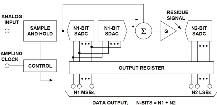
Subranging architecture has been used to reduce the component count and power of flash ADCs [17-19].
A basic two-stage N-bit subranging ADC is shown in Figure 1.2. The ADC is based on two separate conversions, a coarse conversion (N1-bit) in the MSB sub-ADC (SADC) and a fine conversion (N2-bit) in the LSB sub-ADC. The conversion process begins with the sample-and-hold circuit in the hold mode followed by a coarse N1-bit SADC conversion of the MSBs. The digital outputs of the MSB converter drive an N1-bit sub-DAC (SDAC) which generates a coarsely quantized version of the analog input signal. The output of the N1-bit SDAC is subtracted from the held analog input, amplified and applied to the N2-bit LSB SADC. The
amplifier provides gain, G, sufficient to make the residue signal exactly filled the input range of the N2-bit SADC. The output data from the N1-bit SADC and N2-bit SADC are latched into the output registers yielding the N-bit digital output code, where N = N1 + N2.
Figure 1.2 N-bit Two-Stage Subranging ADC.
Pipelined ADC
The term “pipelined” architecture refers to the ability of one stage to process data from the previous stage during any given clock cycle. At the end of each phase of a particular clock cycle, the output of a given stage is passed on to the next stage using the sample-and-hold (S/H) functions and new data is shifted into the stage.
Figure 1.3 (a) shows a pipelined ADC designed with identical stages of k-bit each. This architecture uses the same core hardware in each stage. Figure 1.3 (b) shows the simplest form of this architecture where k = 1.
Design complexity of the pipelined ADC increases linearly, rather than exponentially, with the number of bits [20].
It is often erroneously assumed that all subranging ADCs are pipelined. While it is true that most modern subranging ADCs are pipelined in order to achieve the maximum possible sampling rate, they don’t necessarily have to be pipelined if designed for use at much lower speed.
VIN S/H
A/D D/A
2k + +
- D/A
2 -
k-bit
2k
S/HA/D S/H
A/D D/A + +
- D/A
- k-bit
k-bit
VIN S/H
A/D D/A
2k + +
- D/A
2 -
k-bit
2k
S/HS/HA/D S/H
A/D D/A + +
- D/A
- k-bit
k-bit
VIN S/H
A/D D/A + 2 +
- D/A
- 1-bit
2
S/HA/D S/H
A/D D/A + +
- D/A
- 1-bit
1-bit
VIN S/H
A/D D/A + 2 +
- D/A
- 1-bit
2
S/HS/HA/D S/H
A/D D/A + +
- D/A
- 1-bit
1-bit
(a) k-bit per stage
(b) 1-bit per stage
Figure 1.3 Basic Pipelined ADC with Identical Stages.
Successive Approximation ADC
Figure 1.4 shows the basic successive approximation architecture [21-23]. It performs conversion on command. The “CONVERT START” command places the sample-and-hold (SHA) in the hold mode, and all the bits of the successive approximation register (SAR) are reset to “0” except the MSB which is set to “1”.
The SAR output drives the internal DAC. If the DAC output is greater than the analog input, this bit in the SAR is reset, otherwise it is left set. The next most significant bit is then set to “1”. If the DAC output is greater than the analog input, this bit in the SAR is reset, otherwise it is left set. The process repeats with each bit in turn. When all the bits have been set, tested, and reset or not as appropriate, the contents of the SAR correspond to the value of the analog input and the conversion is complete. The end of conversion is generally indicated by an end-of-convert (EOC) signal.
SAR LOGIC
ANALOG INPUT
DIGITAL OUTPUT COMPARATOR
SHA
DAC
TIMING
EOC CONVERT
START
Figure 1.4 Basic Successive Approximation ADC.
The basic algorithm used in the successive approximation ADC conversion process dates back to the 1500s relating to the solution of a certain mathematic puzzle relating to the determination of an unknown weight by a minimal sequence of weighing operations [24]. In this problem, the object is to determine the least number of weights which would serve to weigh an integral number of pounds from 1 lb to 40 lb using a balance scale. One solution put forth by the mathematician Tartaglia in 1556, was to use the series of weights 1 lb, 2 lb, 4 lb, 8 lb, 16 lb, and 32 lb. The proposed algorithm is the same as used in modern successive approximation ADCs. This solution will actually measure unknown weights up to 63 lb rather than 40 lb as stated in the problem. The algorithm is shown in Figure 1.5 where the unknown weight is 45 lb. The balance scale analogy is used to demonstrate the algorithm.
Figure 1.5 Successive Approximation ADC Algorithm.
Sigma-Delta ADC
The basic single and multi-bit first order sigma-delta ADC architecture is shown in Figure 1.6 (a) and (b), respectively. The comparator output is converted back to an analog signal with a 1-bit DAC (a comparator), and subtracted from the input signal. The error signal passes through an integrator. The basic oversampling sigma-delta modulator increases the overall signal-to-noise ratio at low frequencies by shaping the quantization noise such that most of it occurs outside the bandwidth of interest. The digital filter then removes the noise outside the bandwidth of interest, and the decimator reduces the output data rate back to the Nyquist rate [25, 26].
(a) Single-bit
(b) Multi-bit (a) Single-bit
(b) Multi-bit
Figure 1.6 Single and Multi-bit Sigma-Delta ADC.
Each of the ADC architectures has its merit and demerit since there always exist tradeoffs between conversion speed, resolution, power consumption, size, static performance, dynamic performance and cost.
Depending on applications, some performance features may be more significant than others. For example, precision sensor conditioning requires high-resolution high-accuracy and low-cost ADCs, but speed and power requirements can be quite loose. Serial link communication system requires very high sampling rate but resolution and power consumption are not first concerns. Figure 1.7 shows a number of applications which have different requirements of ADC sampling rate and resolution.
0 2 4 6 8 10 12 14 16 18 20 22 24
0 10 20 30 40 50 60 70
10k 100k 1M 10M 100M 1G 10G 100G
UWB Video
WLAN Precision
Sensor Audio
Optical Comm.
Bluetooth
Serial Link GSM
VDSL2
Sampling Rate (S/s)
Resolution (bit)
Figure 1.7 ADC Applications.
Figure 1.8 shows each ADC architecture’s dominating area in terms of sampling rate and resolution.
Sigma-delta ADCs are used predominantly in low speed applications, trading speed for resolution by oversampling. Successive-approximation-register (SAR) ADCs are frequently the architecture of choice for medium-to-high-resolution applications, typically with low-to-medium sampling rates. Pipelined ADC has become the most popular ADC architecture for sampling rates from a few MS/s up to a hundred MS/s, with medium-to-high resolutions. Subranging architecture is a cross between the pipelined and flash architectures.
Flash ADCs are suitable for applications requiring very large bandwidths yet low resolutions. Time interleaving (TI) architecture is used to combine with other architectures to multiply the sampling rate.
0 2 4 6 8 10 12 14 16 18 20 22 24
0 10 20 30 40 50 60 70
10k 100k 1M 10M 100M 1G 10G 100G Sampling Rate (S/s)
Resolution (bit)
Flash
Folding Pipeline SAR
Sigma-delta
TI+αααα
Figure 1.8 ADC Architectures Domain Area.
1.2 Research Motivation
Despite the variety of ADC architectures utilized in diverse applications, their performances are usually summarized by a relatively small number of parameters: stated resolution, signal-to-noise ratio (SNR), signal-to-noise-and-distortion ratio (SNDR), effective number of bits (ENOB), sampling rate, and power consumption. In 1999, Walden’s survey of more than 150 converters concluded ADC performance limitations [27]. For low speed ADCs, resolution appears to be limited by thermal noise. For medium-to-high speed ADCs, approximately one bit of resolution is lost for every doubling of the sampling rate. For very high speed ADCs, the speed of device technology is a limiting factor due to comparator ambiguity. In the survey paper, an ADC figure of merit (FOM) was firstly defined as2ENOB× fsampling/Power. A modified version of the Walden FOM has been more widely accepted, which is shown as follows.
sampling ENOB f
Power
FOM = ×
2 (1.1) Figure 1.9 plots the experimental ADCs which have been presented in the world’s top two solid-state-circuit conferences in the past decade [28]. Many ADC architectures and integrated circuit technologies have been proposed and implemented to push back performance limits. Although different metrics and interpretations of ADC performances may be used in different research work, an overall trend is not affected in a significant way. The trend that cuts across nearly all resolutions and sampling rates is “low power”. The average FOM becomes smaller and smaller, indicating lower energy consumed in each effective conversion step. In this work a 9-bit 100-MS/s ADC has been designed and implemented with power consumption of only 1.46 mW, resulting in an FOM of 39 fJ/conv-step, which is one of the best-performing converters in the world.
This work targets battery-powered data communication and imaging processing systems. ADCs with medium resolution (8-bit to 10-bit) and moderate sampling rate (several tens to hundred of MHz) are required for applications such as one-segment digital TV receiver in cell phones, high definition camcorders, and etc.
Today’s portable consumer electronics devices require designs of professional-quality sound, display and high definition video with lower power consumption, smaller area, more functions and lower cost. Therefore,
energy efficient and area efficient ADCs with high performance are in great demand.
Pipelined and SAR architectures are most commonly selected for in the range of moderate resolution and speed. As introduced in the previous section, pipelined ADCs rely on inter-stage amplifiers, which are usually operational amplifiers (op-amp), to accurately amplify the residue signal in each stage. However, with technology scaling, low power design of pipelined ADC with op-amps has become more challenging, because the achievable gain per stage is limited by transistor short-channel effects and reduction of power supply voltage. On the other hand, in SAR architecture, only one single comparator decides the digital outputs bit by bit. Since the only active analog component is the comparator, which does not need to be linear, the major power consumption is in the digital circuits. Digital power and speed benefit from the technology scaling, making SAR architecture a power-efficient selection. However, a problem with SAR architecture is that they usually cannot deliver the best possible performance when considering about absolute speed, resolution and input capacitance simultaneously. The hundreds of ADCs in Figure 1.9 are filtered by selecting the pipelined and SAR architectures with moderate speed and resolution and re-plotted in Figure 1.10. As shown in Figure 1.10(a), the SAR ADCs have achieved much higher energy efficiency than the pipelined ones, but they all operate at sampling rates lower than 50MS/s. On the other hand, the pipelined architecture is able to achieve sampling rates higher than 100MS/s. This work has focused attention on SAR architecture and proposed several techniques to improve the speed while keeping high energy efficiency. This work has also made efforts to minimize the ADC area to meet the requirements of portable electronic devices, as shown in Figure 1.10(b).
1.E-01 1.E+00 1.E+01 1.E+02 1.E+03 1.E+04 1.E+05 1.E+06 1.E+07
10 20 30 40 50 60 70 80 90 100 110 120
ISSCC 1997-2009 VLSI 1997-2009 FOM=1pJ/conv-step FOM=100fJ/conv-step FOM=10fJ/conv-step
SNDR (dB)
Power/Sampling rate (pJ)
This work
1.E-01 1.E+00 1.E+01 1.E+02 1.E+03 1.E+04 1.E+05 1.E+06 1.E+07
10 20 30 40 50 60 70 80 90 100 110 120
ISSCC 1997-2009 VLSI 1997-2009 FOM=1pJ/conv-step FOM=100fJ/conv-step FOM=10fJ/conv-step
SNDR (dB)
Power/Sampling rate (pJ)
This work
Figure 1.9 Trend of ADC Performance in the Past Decade.
1 10 100 1000
0.E+00 5.E+07 1.E+08 2.E+08 2.E+08
SAR Pipelined
0 50 100 150 200 Sampling Rate (MS/s)
1000
100
10
1
Energy Efficiency (fJ/conv)
U. Twente
ChengKung U.
IMEC This work
STMicro MIT
Stanford
Fujitsu
POSTECH IMEC U. Pavia MIT
UCSD
MediaTek UTAustin Fujitsu
U. Toronto Sharp Infineon MIT U. Michigan
Samsung
(a)
0.01 0.1 1 10
6 7 8 9 10 11 12
SAR Pipelined
6 7 8 9 10 11 12 Effective Number of Bits
10
1
0.1
0.01 Die Area (mm2 )
This work
U. Twente MIT IMEC ChengKung U.
IMEC POSTECH
U. Pavia
U. MichiganMIT
STMicro Stanford
MIT Sogang U.
UCSD OSU
MediaTek
Infineon Fujitsu Samsung
MIT
0.01 0.1 1 10
6 7 8 9 10 11 12
SAR Pipelined
6 7 8 9 10 11 12 Effective Number of Bits
10
1
0.1
0.01 Die Area (mm2 )
This work
U. Twente MIT IMEC ChengKung U.
IMEC POSTECH
U. Pavia
U. MichiganMIT
STMicro Stanford
MIT Sogang U.
UCSD OSU
MediaTek
Infineon Fujitsu Samsung
MIT
(b)
Figure 1.10 Target ADC Performance (a) Energy Efficiency vs. Sampling Rate (b) Die Area vs. ENOB.
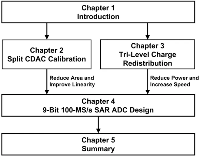
1.3 Dissertation Organization
This thesis is organized as shown in Figure 1.11.
Chapter 1 is an introduction of the study, which includes the data converter background, research motivation and dissertation organization.
Chapter 2 presents a split capacitive DAC calibration scheme, which can be used to reduce area and input load capacitance while keeping good linearity performance. The issues of conventional split CDACs are analyzed, followed by the principle and implementation of the proposed calibration method. The feasibility is proved by the test chip measurement results.
Chapter 3 presents the tri-level charge redistribution scheme. The switching energy inefficiency and settling problem of the conventional method are first analyzed. Then the tri-level method and differential capacitor bottom-plate charge-sharing technique are introduced in details. The improvement of energy efficiency and settling speed are shown in simulation results.
Chapter 4 presents a high performance SAR ADC design, which combined the split CDAC calibration and the tri-level charge redistribution techniques. Circuit design details of each building block are provided.
The ADC test chip implemented in a stand CMOS process is measured and compared with other state-of-the-art converters.
Chapter 5 summarizes the thesis and provides a prospect of future work.
Chapter 1 Introduction
Chapter 4
9-Bit 100-MS/s SAR ADC Design Chapter 2
Split CDAC Calibration
Reduce Area and Improve Linearity
Chapter 5 Summary
Chapter 3 Tri-Level Charge
Redistribution
Reduce Power and Increase Speed
Figure 1.11 Dissertation Organization.
References
[1] W. Kester, "The data conversion handbook," Analog Devices, 2005.
[2] P. M. Rainey, "Facsimile Telegraph System," U.S. Patent 1,608,527, filed July 20, 1921, issued November 30, 1926.
[3] A. H. Reeves, "Electric Signaling System," U.S. Patent 2,272,070, filed Nov. 22, 1939, issued Feb. 3, 1942.
Also French Patent 852,183 issued 1938, and British Patent 538,860 issued 1939.
[4] J. C. Schelleng, "Code Modulation Communication System," U.S. Patent 2,453,461, filed Jun. 19, 1946, issued Nov. 9, 1948.
[5] W. M. Goodall, "Telephony by Pulse Code Modulation," Bell System Technical Journal, Vol. 26, pp.
395-409, Jul. 1947.
[6] R. W. Sears, "Electron Beam Deflection Tube for Pulse Code Modulation," Bell System Technical Journal, Vol. 27, pp. 44-57, Jan. 1948.
[7] J. O. Edson and H. H. Henning, "Broadband Codecs for an Experimental 224Mb/s PCM Terminal," Bell System Technical Journal, Vol. 44, pp. 1887-1940, Nov. 1965.
[8] R. Staffin and R. D. Lohman, "Signal Amplitude Quantizer," U.S. Patent 2,869,079, filed Dec. 19, 1956, issued Jan. 13, 1959.
[9] T. C. Verster, "A Method to Increase the Accuracy of Fast Serial-Parallel Analog-to-Digital Converters,"
IEEE Transactions on Electronic Computers, EC-13, pp. 471-473, 1964.
[10] D. J. Kinniment, D. Aspinall, and D.B.G. Edwards, "High-Speed Analogue-Digital Converter," IEE Proceedings, Vol. 113, pp. 2061-2069, Dec. 1966.
[11] C. C. Cutler, "Transmission Systems Employing Quantization," U.S. Patent 2,927,962, filed Apr. 26, 1954, issued Mar. 8, 1960.
[12] H. Inose, Y. Yasuda, and J. Murakami, "A Telemetering System by Code Modulation: ∆-Σ Modulation,"
IRE Transactions on Space Electronics Telemetry, Vol. SET-8, pp. 204-209, Sep. 1962. Reprinted in N. S.
Jayant, Waveform Quantization and Coding, IEEE Press and John Wiley, ISBN 0-471-01970-4, 1976.
[13] W. C. Black Jr. and D. A. Hodges, “Time Interleaved Converter Arrays,” IEEE International Conference on Solid State Circuits, pp. 14-15, Feb. 1980.
[14] J. Peterson, "A Monolithic video A/D Converter," IEEE Journal of Solid-State Circuits, Vol. SC-14, No. 6, pp. 932-937, Dec. 1979.
[15] Yukio Akazawa et al., “A 400MSPS 8 Bit Flash A/D Converter,” IEEE ISSCC Digest of Technical Papers, 1987, pp. 98-99.
[16] Chuck Lane, “A 10-bit 60MSPS Flash ADC,” IEEE Proceedings of the Bipolar Circuits and Technology Meeting, Sep. 1989, pp. 44-47.
[17] J. L. Fraschilla, R. D. Caveney, and R. M. Harrison, "High Speed Analog-to-Digital Converter," U.S.
Patent 3,597,761, filed Nov. 14, 1969, issued Aug. 13, 1971.
[18] O. A. Horna, "A 150Mbps A/D and D/A Conversion System," Comsat Technical Review, Vol. 2, No. 1, pp. 52-57, 1972.
[19] R. Gosser and F. Murden, "A 12-bit 50MSPS Two-Stage A/D Converter," ISSCC Digest of Technical Papers, 1995, pp. 278-279.
[20] S. H. Lewis, S. Fetterman, G. F. Gross, Jr., R. Ramachandran, and T. R. Viswanathan, “A 10-b 20-Msample/s Analog-Digital Converter,” IEEE Journal of Solid-State Circuits, Vol. 27, No. 3, pp. 351-358, Mar. 1992.
[21] H. R. Kaiser, et al, "High-Speed Electronic Analogue-to-Digital Converter System," U.S. Patent 2,784,396, filed Apr. 2, 1953, issued Mar. 5, 1957.
[22] Bernard M. Gordon and Evan T. Colton, "Signal Conversion Apparatus," U.S. Patent 2,997,704, filed Feb.
24, 1958, issued Aug. 22, 1961.
[23] J. McCreary and P. Gray, “All-MOS charge redistribution analog-to-digital conversion techniques,”
IEEE Journal of Solid-State Circuits, vol. SC-10, no. 12, pp. 371–379, Dec. 1975.
[24] W. W. Rouse Ball and H. S. M. Coxeter, "Mathematical Recreations and Essays," Thirteenth Edition, Dover Publications, pp. 50-51, 1987.
[25] C. B. Brahm, "Feedback Integrating System," U.S. Patent 3,192,371, filed Sep. 14, 1961, issued Jun. 29,
1965.
[26] R. J. van de Plassche, "A Sigma-Delta Modulator as an A/D Converter," IEEE Transactions on Circuits and Systems, Vol. CAS-25, pp. 510-514, Jul. 1978.
[27] R. H. Walden, “Analog-to-Digital Converter Survey and Analysis”, IEEE Journal on Selected Areas in Communications, vol. 17, no. 4, pp. 539-550, Apr. 1999.
[28] B. Murmann, "ADC Performance Survey 1997-2010," [Online] Available:
http://www.stanford.edu/~murmann/adcsurvey.html.
Chapter 2 Split Capacitor DAC Calibration
2.1 Charge Redistribution SAR ADC
Successive approximation ADC has a simple structure, low power consumption and reasonably fast conversion rate. The overall accuracy and linearity of the successive approximation ADC is determined primarily by the internal DAC. Until recently, most precision SAR ADCs used laser-trimmed thin-film resistor DAC to achieve the desired accuracy and linearity [1]. The thin-film resistor trimming process makes the chip larger and more expensive, and the thin-film resistor values may be affected when subjected to the mechanical stresses of packaging. The development of sub-micron CMOS process has made possible very small, cheap and accurate switched-capacitor (or charge redistribution) DACs, which have become popular in successive approximation ADCs [2-5]. The advantage of the charge redistribution DAC is that the accuracy and linearity is mainly determined by high-accuracy photolithography, which in turn controls the capacitor plate area and the capacitance as well as matching. In addition, small capacitors can be placed in parallel with the main capacitors which can be switched in and out under control of auto-calibration routines to achieve high accuracy and linearity without the need for thin-film laser trimming. The use of capacitive charge redistribution DAC offers another advantage as well. The DAC itself serves as a sample-and-hold (SHA) circuit, and therefore neither an external SHA nor allocation of chip area for a separate internal SHA is required.
An N-bit charge redistribution SAR ADC is shown in Figure 2.1. The switches are shown in the sampling mode where the analog input voltage VIN is constantly charging and discharging the parallel combination of all the capacitors. The conversion mode is initiated by opening switch SC, storing the voltage VBIAS–VIN on the capacitor array. The voltage at node P is allowed to move as the bit switches are manipulated.
Then the MSB capacitor is connected to VREF while the rest capacitors are connected to ground, causing the node P to settle to
2
REF IN
BIAS P
V V V
V = − + (2.1) The comparator then makes the decision of the MSB, and the SAR logic leaves the MSB capacitor connected
to VREF or connects it to ground depending on the comparator output, which is low or high depending on whether the voltage at node P is negative or positive.
1
2
REF IN
V >V
MSB = (2.2) 0
2
REF IN
V <V
A similar process is followed for the remaining two bits. At the end of the conversion interval, all the capacitors are connected to VIN, SC is connected to ground, and the converter is ready for another cycle.
The extra LSB capacitor (dummy capacitor) as shown in Figure 2.1 is required to make to total value of the capacitor array equal to 2N ⋅C in the case of the N-bit DAC so that the binary division is accomplished when the individual bit capacitors are manipulated.
VIN VREF
SAR LOGIC CLK
DOUT 2N-1C
2C C
C
+ -
LSB MSB SC
P
2ndLSB
VBIAS VBIAS
Figure 2.1 Charge Redistribution SAR ADC.
2.2 Split Capacitor DAC
Charge redistribution SAR ADC has an inherent sample-and-hold function. However, the input load capacitance and area of a binary-weighted capacitor DAC (CDAC) increase exponentially with the number of bits. Split capacitor arrays have been proposed as solutions to reduce both input capacitance and area [6-9].
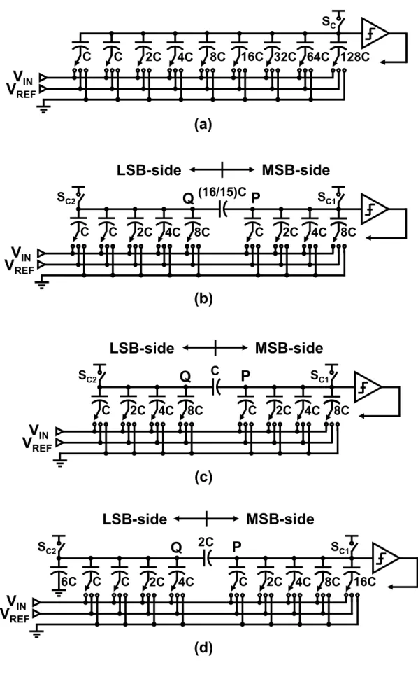
Figure 2.2 shows an 8-bit example. Figure 2.2(a) is a binary-weighted CDAC, where C represents the unit capacitance. The total input capacitance is equal to 256C and the total area is 256 times the unit capacitor area.
The asymmetric symbol of capacitors indicates that top and bottom capacitor plates have different parasitic capacitance. Generally speaking, it is preferable to connect the capacitor plate with smaller parasitic capacitance to the comparator input.
In Figure 2.2(b), a bridge capacitor is implemented to connect two split capacitor arrays which have the same scaling. The left array is the lower weight side (LSB-side) and the right array is the higher weight side (MSB-side). The bridge capacitor has a fractional value equal to (16/15)C which is determined by the resolution of the LSB-side capacitor array [6]. In the charge-redistribution process, the total weight of the LSB-side capacitor array is ideally equal to the weight of the lowest bit in the MSB-side capacitor array. Note that the dummy capacitor C is only implemented in the L-side array. During the sampling mode, all the capacitors in the LSB-side and MSB-side arrays are connected to the analog input signal VIN, and both switches SC1 and SC2 are connected to an ac ground (a dc bias voltage determined by the comparator input common mode voltage). The total input load capacitance is equal to 31C, which is about 8 times smaller than the binary-weighted capacitor array. The area reduction is also 8 times. However, the bridge capacitor being fractional causes poor matching with the other capacitors. Parasitic capacitance at node Q affects the charge coupling ratio of the LSB-side array and the bridge capacitor. Both above problems degrade the DAC linearity and thus the overall ADC linearity performance.
![Figure 1.4 shows the basic successive approximation architecture [21-23]. It performs conversion on command](https://thumb-ap.123doks.com/thumbv2/123deta/6083823.2081422/20.892.99.798.584.1089/figure-shows-successive-approximation-architecture-performs-conversion-command.webp)