of traps in hybrid organic‑inorganic perovskites
Author Andrew Winchester Degree Conferral
Date
2020‑10‑31
Degree Doctor of Philosophy Degree Referral
Number
38005甲第62号 Copyright
Information
(C) 2020 The Author.
URL http://doi.org/10.15102/1394.00001604
Creative Commons Attribution‑NonCommercial 4.0 International(https://creativecommons.org/licenses/by‑nc/4.0/)
Okinawa Institute of Science and Technology Graduate University
Thesis submitted for the degree
Doctor of Philosophy
Spatially and temporally resolved microscopy of traps in hybrid
organic-inorganic perovskites
by
Andrew J. Winchester
Supervisor: Keshav M. Dani
October, 2020
Declaration of Original and Sole Authorship
I, Andrew J. Winchester, declare that this thesis entitled Spatially and temporally resolved microscopy of traps in hybrid organic-inorganic perovskites and the data pre- sented in it are original and my own work.
I conrm that:
No part of this work has previously been submitted for a degree at this or any other university.
References to the work of others have been clearly acknowledged. Quotations from the work of others have been clearly indicated, and attributed to them.
In cases where others have contributed to part of this work, such contribution has been clearly acknowledged and distinguished from my own work.
None of this work has been previously published elsewhere, with the exception of the following:
"Performance-limiting nanoscale trap clusters at grain junctions in halide perovskites", T. A. S. Doherty, A. J. Winchester, et al., Nature 580, 360-366 (2020)
Date: October, 2020 Signature:
iii
Abstract
Spatially and temporally resolved microscopy of traps in hybrid organic-inorganic perovskites
In recent years the class of materials known as hybrid organic-inorganic perovskite (HOIP) have received notable attention for use in photovoltaic applications, with record solar conversion eciencies reaching other established thin lm systems. Despite their rapid development, there are still ongoing issues related to heterogeneous lm prop- erties which limit device performance. It has been suggested that sites which capture charge carriers (traps) could be localized on a micrometer or smaller size scale, leading to regions of poor eciency. Understanding the electronic properties of such regions, in particular on how they inuence carrier recombination, will therefore provide cru- cial information about the carrier loss pathways in HOIP lms, which will be essential for developing new strategies to minimize losses and create more ecient devices. In order to gain information about the ultrafast charge carrier recombination dynamics on nanoscale length scales, specialized techniques which can provide information with both high spatial and temporal resolution will be necessary. Here, we utilize time re- solved photoemission electron microscopy (TR-PEEM) as a novel technique to study the nanoscale ultrafast properties of photo excited carriers and their relation to hetero- geneous lm properties in HOIP thin lm materials. Following this overall theme, the work in this thesis will address several nanoscale properties and phenomenon. First, we will uncover the nanoscale distribution of carrier traps in a HOIP lm which result in non-radiative losses. We then will describe in depth the ultrafast carrier trapping processes happening at nanoscale trap clusters. Following this, we will then discuss other novel information and studies on the traps in HOIP which can be realized using TR-PEEM, namely on eects of light treatments and morphological information. By gaining a deeper understanding in these directions, we hope to contribute to the broader goal of improving HOIP photovoltaic device eciency and showcase TR-PEEM as a novel technique for studying photocarrier dynamics in semiconductor materials.
v
Acknowledgment
This thesis work would not have been possible without the contributions of so many people, whom I would like to acknowledge below.
I would rst like to thank Stuart Macpherson (Cambridge) for helping to analyze and interpret the trapping kinetics and for his ideas, help, and work in the project studying light-soaking eects using PEEM, which we worked together on during his visit to OIST under a JSPS fellowship. I also thank him for providing perovskite samples and taking photoluminescence data. In addition, I want to also thank him for his help in preparing the rst manuscript submitted from this thesis work, as well as for all the fruitful and interesting scientic discussions related to perovskites and TR-PEEM.
I would next like to thank Tiarnan Doherty (Cambridge) for his discussions about perovskite materials, in particular about their nanoscale properties such as strain, composition, and crystal structure. I thank him immensely for his part of our collab- orative work to understand these properties as related to my PEEM and TR-PEEM results, which has resulted in our shared rst-authorship Nature paper, which he also contributed writing to.
I thank Dr. E Laine Wong (OIST) for working together with me during the begin- ning of my thesis work as we learned and developed the instrumentation, analysis, and interpretation behind using the TR-PEEM technique at OIST. I also want to thank her for teaching me about ultrafast optics and for mentoring me as the senior (and rst) graduate student from our group.
I next thank Vivek Pareek (OIST), who was largely responsible for building the third and fourth harmonic generation setup used throughout this thesis work in PEEM and TR-PEEM measurements, without which most, if not all of the measurements shown here would have been impossible or impractical. I also thank him for taking photoluminescence data, for many discussions about ultrafast carrier recombination processes and interactions in semiconductors, and lastly for moral support during my thesis work.
I also thank Dr. Mojtaba Abdi-Jalebi (Cambridge) and Zahra Andaji-Gamaroudi (Cambridge) for preparing and sending perovskite samples, especially at the beginning of this thesis work.
I would also like to thank Sonya Kosar (OIST) for learning and continuing to explore with TR-PEEM several of the ideas and directions started from this thesis work, as well as for moral support. In particular, I want to thank her for her work in taking and analyzing the high-resolution PEEM images which contributed greatly towards our publication in Nature.
vii
I next need to thank Dr. Michael Man (OIST) for teaching me so much of the detail and intricacies behind using, maintaining, and interpreting LEEM and PEEM experiments and instrumentation. I also thank him for his hard work in establishing TR-PEEM within our group. I thank him for his help with interpretation and analysis of data, including help with computer programming. I lastly thank him for being a scientic role model and mentor for me during my thesis.
I next thank Dr. Julien Madéo (OIST) for teaching me so much about ultrafast optics, lasers, and carrier recombination processes in condensed matter. I also thank him for helping Vivek Pareek to build and design the third and fourth harmonic gen- eration setup. Lastly, I thank him for his help in keeping the laser system central to my experiments running in good condition and teaching me how to maintain it.
I thank Dr. Chris Petoukho (OIST) for his help with interpreting data and for his discussions about perovskite and organic photovoltaic materials.
I thank Prof. Bala Murali Krishna Mariserla (OIST) for teaching me about ultrafast optics and laser systems.
I thank Prof. Samuel Stranks (Cambridge) for providing us the opportunity to study his group's perovskite material, helping interpret our results and to identify and direct the interesting and relevant points of our results to the perovskite community.
I also thank him for his help with preparing the rst manuscript submitted from this thesis work and for many useful and interesting discussions about perovskite materials and photovoltaic applications.
In, addition, I would like to thank Prof. Samuel Stranks and the rest of his group at Cambridge for their hospitality and interesting scientic discussions during my visit there.
I would lastly like to thank Prof. Keshav Dani (OIST) for providing me the oppor- tunity to undertake a very unique and challenging thesis project in his group and for his help in directing this research for the very young eld of TR-PEEM in semiconduc- tors, which has been a very challenging and rewarding task for everyone involved. I thank him for his guidance in directing, analyzing, and interpreting the research. I also thank him for teaching me about ultrafast optics and lasers, his help with preparing the manuscript submitted from this thesis work, as well as his help and guidance in writing scientic documents, preparing for conference presentations, and in choosing career paths.
I especially want to thank Prof. Keshav Dani for creating the environment of the Femtosecond Spectroscopy Unit (FSU) at OIST, who has become like a second family.
Together, the FSU has shared in the joys, excitement, and hardships of research at a newly established university. I am deeply grateful for the support of the FSU during my thesis work.
And last, but not least, I also thank my parents and family for their love and support throughout my thesis work. I deeply appreciate that they have continued supporting me throughout my academic life so far, even despite being a (literal) world apart after moving to Japan for my thesis.
皆さん、本当にありがとうございました!
Abbreviations
AFM atomic force microscopy
ARPES angle resolved photoemission spectroscopy BBO beta barium borate
BP band pass Br bromine
CB conduction band CCD charge coupled device
Cs cesium
EQE external quantum eciency eV electron volt
FA formamidinium FOV eld of view
fs femtosecond FTO uorine tin oxide
FWHM full width at half maximum GaAs gallium arsenide
HeNe Helium Neon
HOIP hybrid organic-inorganic perovskite I-Br iodine and bromine mixed cation HOIP I-only iodine only mixed cation HOIP
IR infrared
ITO indium tin oxide
K-pass potassium passivated mixed cation mixed halide HOIP LED Light Emitting Diode
LEEM low energy electron microscopy MA methylammonium
MAPbI3 methylammonium lead iodide nm nanometer
ns nanosecond O2 oxygen (gas) Pb lead
PEEM photoemission electron microscopy PL photoluminescence
ps picosecond PV photovoltaic QE quantum eciency
ix
SED scanning electron diraction SEM scanning electron microscopy
SRH Shockley-Read-Hall
TEM transmission electron microscopy
TR-PEEM time-resolved photoemission electron microscopy UHV ultra high vacuum
UPS ultraviolet photoelectron spectroscopy UV ultraviolet
VB valence band XRD x-ray diraction
XRF x-ray uorescence
XPS x-ray photoelectron spectroscopy
Contents
Declaration of Original and Sole Authorship iii
Abstract v
Acknowledgment vii
Abbreviations ix
Contents xi
List of Figures xiii
List of Tables xv
Introduction 1
1 Hybrid organic-inorganic perovskites 3
1.1 Photovoltaic properties and development of HOIP . . . 3
1.2 Fundamental limits and issues . . . 4
1.3 Triple cation perovskite . . . 6
2 Time resolved photoemission electron microscopy 11 2.1 Photoemission electron microscopy . . . 11
2.1.1 General photoemission process . . . 11
2.1.2 Photoemission microscopy . . . 13
2.2 Time-resolved photoemission electron microscopy . . . 17
2.3 Considerations for TR-PEEM . . . 22
2.3.1 Space Charge . . . 22
2.3.2 Laser Noise . . . 24
2.3.3 Signal Interpretation . . . 26
2.4 PEEM Discussion . . . 28
3 Photoemission microscopy and spectroscopy of HOIP 29 3.1 PEEM imaging of heterogeneity . . . 29
3.2 Photoemission spectroscopy of trap states . . . 32
3.3 Discussion of trap origins and implications . . . 36 xi
4 Steady-state recombination losses 39
4.1 PL microscopy . . . 39
4.2 Correlations between PL and trap sites . . . 42
4.3 Non-radiative loss discussion . . . 44
5 Time-resolved microscopy of trapping dynamics 47 5.1 Time Resolved Imaging . . . 47
5.2 Trapping Kinetics . . . 52
5.2.1 Fluence Dependence . . . 52
5.2.2 Trap Assisted Auger . . . 56
5.2.3 Diusion Limited Trapping . . . 60
5.3 Time-resolved discussion . . . 69
6 Light and Environmental Control of Traps 71 6.1 In-situ light exposure . . . 71
6.2 Ex-situ environmental exposure . . . 74
6.3 Light-treatment Discussion . . . 77
7 Film morphology from PEEM 81
Conclusion 85
Bibliography 87
List of Figures
1.1 Perovskite Structure . . . 4
1.2 QE SRH rates . . . 5
1.3 Triple Cation Sample . . . 7
1.4 Triple Cation Perovskite Morphology . . . 8
2.1 Photoemission Schematic . . . 12
2.2 PEEM diagram . . . 14
2.3 Time Resolved Photoemission . . . 18
2.4 Laser Spectrum . . . 19
2.5 TR-PEEM Diagram . . . 20
2.6 Space Charge Images . . . 23
2.7 Space Charge Spectrum . . . 23
2.8 Laser Stability and Noise . . . 25
2.9 GaAs signal example . . . 27
3.1 PEEM images of HOIP . . . 30
3.2 Spot statistics . . . 31
3.3 PES of HOIP Traps . . . 33
3.4 PES comparison . . . 34
3.5 Equilibrium energy diagrams . . . 35
4.1 Iodine-only PL map . . . 40
4.2 Iodine-only PL-PEEM overlay . . . 41
4.3 Mixed-halide PL-PEEM overlays . . . 42
4.4 PL-PEEM correlations . . . 43
4.5 PL-PEEM statistics correlations . . . 45
5.1 TR-PEEM Images . . . 48
5.2 TR-PEEM dynamics . . . 49
5.3 Time constant dependence on intensity . . . 51
5.4 Fluence dependent TR-PEEM . . . 53
5.5 Fluence dependence of TR-PEEM tting . . . 55
5.6 Trap Assisted Auger Dynamics . . . 58
5.7 Trap Assisted Auger Coecients . . . 59
5.8 Diusion limited trapping . . . 62
5.9 Kinetic diusion-trapping solutions . . . 64
5.10 Diusion simulation with de-trapping included . . . 65 xiii
5.11 2D Diusion Schematic . . . 67
5.12 2D Diusion Simulation . . . 68
6.1 In-situ Light Soaking Images . . . 72
6.2 In-situ Light Soaking Photoemission Spectroscopy . . . 73
6.3 Ex-situ Light Soaking in Oxygen Images . . . 75
6.4 Ex-situ Light Soaking in Oxygen Photoemission Spectroscopy . . . 76
6.5 Trapping Kinetics after ex-situ Light Soaking in Oxygen . . . 78
7.1 AFM and PEEM comparison . . . 82
7.2 High resolution PEEM imaging . . . 83
List of Tables
5.1 Double exponential t results at xed 1.55 eV pump uences . . . 50
xv
Introduction
Over the course of the latter half of the twentieth and ongoing into the twenty rst cen- tury, there has been a growing push to pursue and develop "green", or more specically, alternate, renewable, and ecient energy sources. In particular, solar cell technologies have been one of the most prominent solutions towards achieving "green" energy. The development of solar cells since the demonstration of practical silicon-based devices by Bell labs in the 1950s [1] is one full of new materials, advanced processing methods, and device design and architecture. However, one of the important challenges, central to the operation of all solar cells and photovoltaic (PV) devices, is overcoming the eects of unwanted charge carrier losses within the absorbing material. In particular, understanding the properties of defects which act as charge carrier trapping and recom- bination centers within the solar material is central to achieving higher device eciency.
Park, et al. [2] recently gave a nice overview of the development of defect understand- ing in silicon, thin-lm, and the currently expanding eld of hybrid organic-inorganic perovskite (HOIP) materials, which underlines the importance of understanding how defects inuence the properties of solar cell devices. One of the surprising discoveries about HOIP materials has been that despite the relatively high density of carrier traps measured (as compared to inorganic photovoltaic materials), quite good performance can be achieved in thin lm devices [3]. However, most HOIP devices still operate in a regime where the eciency is limited by unwanted recombination losses. Hence, under- standing the details behind the properties of defects and their role on carrier trapping has become a greater research focus over the last few years, as solving issues related to carrier traps still represents an important direction for improving future devices.
Stepping back for a moment, it is also important to consider how advances in material understanding have been linked to improvements in experimental tools and techniques. In particular, advances in electron microscopy techniques have seen tremen- dous success for material study. In the last two decades, a new sub-eld of electron microscopy has started to emerge, following the availability of commercial ultrafast pulsed laser sources, which is known generally or loosely as time-resolved or ultrfast electron microscopy. This provides ways to perform high spatial resolution imaging of dynamic events on time scales down to picoseconds, femtoseconds, or potentially even attoseconds, which are the relevant time scales for studying many electronic pro- cesses in materials. The most well known example is that of 4-dimensional electron microscopy using transmission electron microscopy (TEM) [4], where electron pulses are generated and used to image samples. However, there are several related techniques emerging in this eld which oer dierent strengths and possibilities. In particular, the technique of time-resolved photoemission electron microscopy (TR-PEEM) is well
1
suited for studying the nanoscale dynamics of photoexcited carriers in semiconductors [5], where pulses of light are used to emit electrons from the sample itself that are then imaged in the microscope. This technique has only recently started being applied to semiconductor materials, and oers new avenues for understanding the relaxation of excited states in matter and in particular in heterogeneous systems, where nanoscale material dierences, charge transfer, and interactions will be of interest.
With these two general ideas in mind, the overall goal of my thesis work was then to gain insight into the properties and recombination processes of defects in HOIP materials by application of an ultrafast electron microscopy technique, namely TR- PEEM. In the following chapters of this thesis, I will rst discuss in more detail the properties of the HOIP materials studied in relation to their use in solar cell devices and ongoing issues in chapter 1. I will then introduce in depth the methodology behind TR-PEEM and discuss its merits and limits in chapter 2. In chapters 3 and 4, I will show the rst major results of my work on using steady-state PEEM to identify nanoscale traps in HOIP thin lms and their eects on non-radiative carrier losses, respectively. I will then discuss the results of my TR-PEEM measurements in studying the recombination processes at these trap sites in chapter 5. Following the development of our understanding of the traps in these HOIP lms, the last two chapters will focus on other directions and applications of PEEM and TR-PEEM for understanding the defect nature in these lms. In chapter 6, I will show how PEEM can be used to study the light-soaking phenomenon often seen in HOIP lms, while in chapter 7 I will show the possibility for using PEEM to observe the heterogeneous grain morphology in-situ.
Finally, I will end the thesis by summarizing the main results of my work, as well as the ideas and implications arising from them in the conclusion.
Chapter 1
Hybrid organic-inorganic perovskites
The aim of this chapter will be to review and highlight the important properties and discoveries related to hybrid organic-inorganic perovskite (HOIP) materials in order to motivate the research direction of the rest of the thesis. In section 1.1 I will introduce the general properties and use of HOIP materials in relation to their photovoltaic applications. In section 1.2, I will then discuss some of the relevant and ongoing fundamental issues towards their use in solar cells. I will lastly discuss more specically in section 1.3 the general properties of the triple cation samples studied in this thesis.
1.1 Photovoltaic properties and development of HOIP
HOIP are a class of material which has recently seen tremendous interest for use in photovoltaic applications. They follow the general chemical formula for the perovskite crystal structure of ABX3, where the A and B species are cations and the X species is an anion. This forms a crystal structure comprised of BX6 octahedra which surround the A cation, as depicted in gure 1.1. In order to satisfy the perovskite structure, the radii of the dierent ions (RA, RB, RX) generally follow the Goldschmidt tolerance factor t [6], ranging between 0.8 and 1, where t = √RA+RB
2(RB+RX). Perovskites containing organic cations were rst extensively studied starting from the late 1970s [7]. These HOIPs typically have halide anions (X) such as chlorine (Cl−), bromine (Br−), or iodine (I−) and metal cations (B) such as lead (Pb2+) or tin (Sn2+) forming the inorganic part.
The remaining cation (A) is then a small organic molecule such as methylammonium (CH3NH+3, MA+) or formamidinium (HC(NH2)+2, FA+). However, it wasn't until the work by Kojima, et al. in 2009 where the application of HOIPs towards photovoltaic applications was rst demonstrated, resulting in a HOIP-sensitized solar cell with about 3.8% conversion eciency [8].
Following the rst demonstration by Kojima, there was a tremendous increase in using HOIP materials when it was realized they could be fabricated in a thin-lm solid state device [911]. The ability to construct such a solar cell with good eciency is due to the combination of several desirable properties that HOIP materials were found to possess. First and foremost, they have direct band gap transitions with energies between 1.5-3.1 eV [12]. Accordingly, the absorption coecient in the visible part of the spectrum is quite high for these materials, and may also be enhanced due to excitonic
3
Figure 1.1: Crystal structure of perovskite. Green and gray spheres are the A and B cations, while the smaller red spheres are the X anions.
eects [12]. This makes HOIP materials excellent absorbers for much of the solar spectrum and allows even for thin lms (< 1µm) to absorb a large fraction of incident light. Second, it was found that HOIP lms can have moderate charge carrier mobility with carrier lifetimes ranging from tens of nanoseconds to microseconds [13]. These result in large eective carrier diusion lengths, reaching a micrometer or potentially longer [14, 15]. This implies that thin lm HOIP devices should be very ecient at extracting photo-generated carriers from the solar material before they can recombine.
As another boon to their application, the composition of HOIPs can be continuously tuned in many cases by mixing the halide anions. This allows for direct control over the band gap, and leads to interesting applications such as tandem HOIP solar cells and light emitting diode (LED) devices [16]. Lastly, HOIP thin lms can be readily produced through low temperature solution-based fabrication methods [11], making them very attractive for low cost and exible solar cell applications. Together, this combination of properties has lead to the unprecedented development of HOIP solar cells over the last decade, with record device eciencies improving from 3.8% in 2009 [8]
to over 23% in single junction cells in 2019 [17], surpassing other established thin-lm technologies and now competing with single crystal silicon cells.
1.2 Fundamental limits and issues
Despite the rapid development of HOIP based solar cells, there are however several ongoing fundamental and materials-related issues. One, in particular, is the complete understanding of the nature of defects or carrier traps in HOIP [2, 3, 19]. While traps in HOIP are often considered benign compared to traditional inorganic materials [2, 3], especially considering the low-temperature processing methods used, they are still very important to consider for device applications. For example, given the band gap of methylammonium lead iodide (MAPbI3), the prototypical HOIP material, of
1.2 Fundamental limits and issues 5
Figure 1.2: Calculated variation of QE at dierent rates of SRH recombination using equation 1.1. The B and C constants are taken from literature for MAPbI3 [18]. The dashed gray line represents the approximate carrier density generated under a 1-sun illumination. The reduced QE at high carrier density is due to the increased rate of Auger recombination.
about 1.5 eV, a single junction solar cell under ideal conditions is predicted to achieve about 30% conversion eciency [20]. The main limiting factor preventing current cells from reaching this eciency is the presence of non-radiative carrier recombination [20], which acts as a loss channel that results in fewer carriers being harvested by the solar cell. In particular, Shockley-Reed-Hall (SRH) [21] recombination at deep energy levels is expected to contribute signicantly to the losses when the illumination intensity is approximately 1-sun (about 1 W/m2) [20]. Therefore, strategies to reduce or modify the carrier traps in HOIP are essential towards reaching performance limits. For example, as shown in gure 1.2 for dierent rates of SHR recombination, the calculated quantum eciency (QE), or ratio of emitted photons (i.e. useful carrier recombination [20, 22]) to the total carrier recombination can change dramatically at the 1-sun intensity condition (dashed line). Here, the QE is given by:
QE = Bn2
An+Bn2+Cn3 (1.1)
Where n is the carrier density, and A, B, and C are the rate coecients for SRH (monomolecular), radiative (bimolecular), and Auger (many-body) recombination pro- cesses [22]. B and C are generally xed material properties, thus controlling A is the most signicant way to aect the QE at lower carrier densities, as illustrated in g- ure 1.2. Hence, gaining a detailed understanding of carrier traps and how they aect recombination in these materials is necessary for engineering future devices.
One of the more common ways to asses carrier trapping in photovoltaic materials is through photoluminescence (PL) spectroscopy and microscopy. It provides a way to
asses the ratio of emitted photons to the total generated carriers, or external quantum eciency (EQE, related to QE), which can be used to experimentally determine the steady-state recombination rates of the dierent processes [22]. This has been used, for example, to estimate the amount of SRH recombination in HOIP lms [23, 24].
One of the interesting ndings of PL microscopy measurements has been that the apparent carrier losses can have a signicant spatial heterogeneity. Several works have identied that relative EQE can vary between adjacent or nearby material grains, which are often a few 100 nanometers to about a micrometer in size [2529]. However, at this length scale the interpretation of PL measurements becomes more complicated for several reasons. First, PL measurements are limited in spatial resolution by the optical diraction limit to typically around 300 nm, which is often comparable to or a signicant fraction of a single grain. Second, as introduced in section 1.1, measurements have shown that the carrier diusion length can reach micrometers. Thus, there are additional considerations on how individual grains are connected, which will greatly aect how carriers recombine spatially [2729]. For example, two grains, one with a high density of traps, which are connected will eectively reduce the EQE of both grains and make interpretation complicated. Lastly, while PL is a useful tool, it ultimately only gives direct information about the radiative carrier recombination; non-radiative recombination processes have to be inferred. Due to these limitation, there is some disagreement and conicting reports in the literature regarding the role of carrier traps, particularly at the grain boundaries [25, 27, 28], where traps might be expected to play a larger role [30].
To overcome these limitations, there is a need to utilize other methods which can ac- cess the spatial distribution of traps within the lm. In addition, it would be benecial to use methods which can also measure the recombination kinetics on fast time scales.
This requires a method which has high spatial resolution (below visible optical dirac- tion limit), ability to distinguish trap sites, and high temporal sensitivity (femtosecond to picosecond). In light of these requirements, the technique which we are developing to achieve this is time resolved photoemission electron microscopy (TR-PEEM), which I will describe in detail in chapter 2.
1.3 Triple cation perovskite
After discussing the more general properties of HOIP materials in the previous two sections and before moving to the methods and results, I will discuss the properties of the specic samples used for the study in the rest of this thesis work. As mentioned in section 1.1, the ability to use mixtures of the halide ion (X) has been demonstrated for tuning the material properties. Beyond this, more recently it was found that the organic cation (A) can also use mixed compositions. In particular, certain mixtures of MA and FA with a small fraction of cesium (Cs) can satisfy the Goldschmidt toler- ance factor and provide several benets. These include much more stable lms against degradation, more reproducible devices, additional band gap tuning, and reduced seg- regation of mixed halide compositions [3133]. These improvements have resulted in higher performing solar cell devices overall.
Following this, we have chosen to focus our study on these triple cation HOIP
1.3 Triple cation perovskite 7
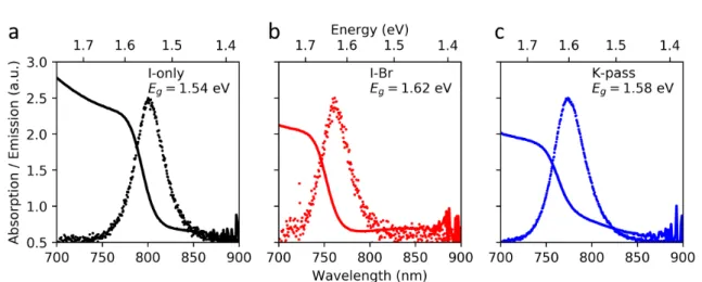
Figure 1.3: Optical characterization of the triple cation samples studied. Absorption (solid lines) and normalized PL emission (dots) from a) iodine only, b) I-Br, and c) K-passivated samples. The band gaps obtained from an extrapolation of the band edge absorption in a Tauc plot are shown in each panel. The absorption was measured with a Thermo Scientic Evolution 600 UV-VIS in transmission geometry. For PL, the excitation wavelength was 532 nm at an intensity of about 4 W/cm2 in a confocal microscope setup (Nanonder30, Tokyo Instruments) and averaged over an area of several micrometers.
lms, which represent the cutting edge in materials development for PV applications.
In this thesis work, I have looked at three slightly dierent compositions, consisting of Cs0.05FA0.78MA0.17PbI3 (iodine-only), mixed halide Cs0.05FA0.78MA0.17Pb(Br0.17I0.83)3
(I-Br), and I-Br with 10% potassium (K) incorporation (K-passivated). These samples were all produced through a low temperature solution-process by our collaborator Prof.
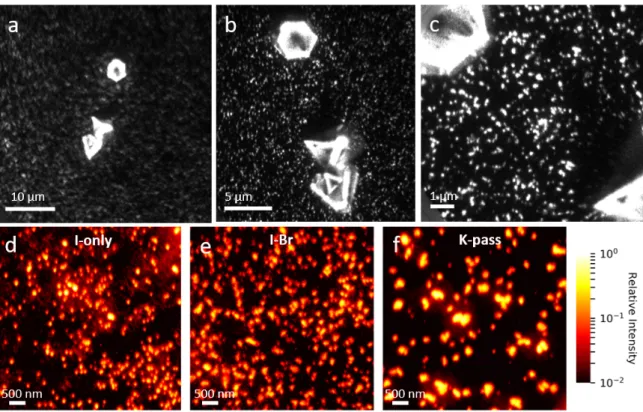
Stranks and his group at Cambridge [34] on indium tin oxide (ITO) or uorine tin oxide (FTO) coated glass substrates. Film thickness were nominally 500 nm. All samples were produced, shipped, and stored under an inert nitrogen atmosphere to prevent exposure to oxygen and water contamination.
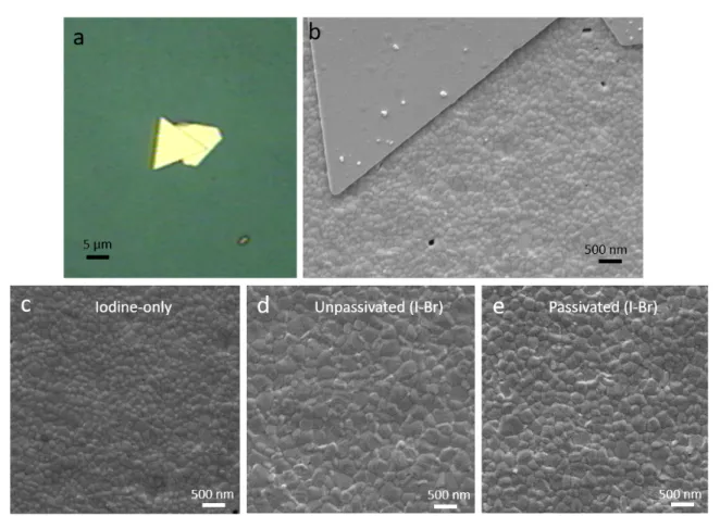
There are two main dierences between these three samples. First, changing the halide ratio and potassium content slightly changes the band gap, as seen from the absorption and PL emission in gures 1.3 a-c. Second, incorporation of potassium greatly improves the radiative eciency by reducing non-radiative losses in the lm [34]. For these samples, we also have solution deposited gold platelets to use as position markers (gure 1.4 a), which allows us to measure the exact same sample area with dierent techniques, for example the scanning electron microscopy (SEM) image in gure 1.4 b. Lastly, I show SEM images of the I-only, I-Br, and K-pass lms in gures 1.4 c, d, and e, respectively. From this, I nd that the typical grain size is around 100-200 nm in the I-only sample, while it is slightly larger for the mixed halide compositions.
Now, following the basic characterization of these lms and after introducing the general issue of understanding traps in these materials, I will spend some time in chapter 2 discussing the technique of TR-PEEM and how it will allow me to provide
Figure 1.4: Morphology of the triple cation perovskite samples for this study. a) optical image of an I-only sample, showing a gold position marker. b) SEM image at 2 kV of the lower part of the same marker, where the grain structure is visible. c, d, e) SEM images at 2 kV, cropped to a 5 µm square for the I-only, I-Br, and K-pass samples.
1.3 Triple cation perovskite 9 insight into some of these issues.
Chapter 2
Time resolved photoemission electron microscopy
In this chapter, the focus will be to build the basis of operating principles and ideas behind time-resolved photoemission microscopy (TR-PEEM). Towards this goal, I will rst introduce the standard photoemission process and principles behind photoemission electron microscopy (PEEM) in section 2.1. Then, I will make the extension to time- resolved measurements in section 2.2. I will then discuss in section 2.3 some of the challenges, limitations, and considerations for performing TR-PEEM measurements.
2.1 Photoemission electron microscopy
The basic operating principle behind PEEM is to image low energy electrons emitted by a material. There are several ways of producing such low energy electrons. Specically for PEEM, as inferred from the name, the photoemission process is the main source of electrons for imaging. Thus, I will rst give some introduction to photoemission before talking specically about how it is used in PEEM imaging.
2.1.1 General photoemission process
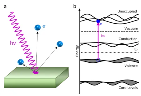
The general process of photoemission is a very well known one, which is an application of the photoelectric eect originally observed, accurately described, and proved in the late 19th century and early 20th century by Hertz, Einstein, and Millikan. The eect states that photons with a large enough energy hν, where h is the Planck constant, impinging upon a material cause emission of electrons, termed photoelectrons, as shown in gure 2.1 a. The resulting photoelectrons escape the material with a kinetic energy KE which depends on the photon energyhν, material work functionφ, and the bound state EB of the electron before it left the material as:
KE =hν−EB−φ (2.1)
For many materials φ is of the order 3-6 electronvolts (eV), and this represents the energy required to remove an electron from the system. This means that for photoemission to occur, the photon energyhν should be at least as large as the work
11
Figure 2.1: General schematic of the photoemission process in a solid. a) UV light (violet wave) with sucient photon energy (hν) can remove electrons (blue spheres) from a material through the photoelectric eect. b) Energy diagram corresponding to the photoemission process in a semiconductor material. UV light (violet line) is absorbed by a material, creating an electron and hole pair (lled and hollow blue circles) in discrete states in the conduction, valence, or core levels. Electrons excited into states above the vacuum level (into the "unoccupied" states) can have sucient kinetic energy to escape the material, as depicted in (a).
2.1 Photoemission electron microscopy 13 function. The photoemission process in solids is commonly described by a three step model, though quantum mechanical treatments (one step model) exist for dealing with strong correlation eects [35]. For this discussion, the three step model is sucient, and is summarized as follows. First, an electron-hole pair is created through absorption of a photon within the energy levels of a material, as shown schematically in gure 2.1 b. Second, the excited electron travels through the material until it reaches a surface.
Third, the excited electron is emitted from the surface, provided it can overcome the material work function.
These three steps include several important practical considerations. In the rst step, absorption of a (discrete!) photon must occur. Therefore, the absorption process must both conserve energy and momentum within the material in order to be allowed.
This means that the likelihood of absorption of a given photon energy hν depends very strongly on the material energy bands, crystal direction, and polarization of light, often referred to by the Fermi Golden Rule. In the second step, events such as electron scattering can change the kinetic energy and momentum of electrons as they travel in the material, leading to the creation of what are known as secondary electrons.
This also limits the eective distance which can be traversed before loosing too much energy to overcome the work function, known as the electron inelastic mean free path [36, 37]. This varies with kinetic energy, and can range from less than a nanometer to several tens of nanometers, implying that photoemission is (in many cases) a surface sensitive probe. In the last step, as mentioned before, the electron can only be emitted if it possesses more kinetic energy than the material work function. As schematically shown in gure 2.1 b, this means that it should occupy a state above the vacuum level (which represents the work function) before exiting the material. Thus, and as outlined in equation 2.1, there are constraints based on the photon energy and work function that determine which bound electron states can emit photoelectrons.
After photoemission, the emitted electron's kinetic energy (and angle) can be mea- sured using various schemes. The resulting energy distributions form the basis for many spectroscopic techniques such as ultraviolet photoelectron spectroscopy (UPS), X- ray photoelectron spectroscopy (XPS) and angle-resolved photoemission spectroscopy (ARPES), which are commonly used to characterize the energy states and elemental composition of materials. As a microscopy technique, the goal of PEEM is to then form a real space image of a surface using such photoelectrons.
2.1.2 Photoemission microscopy
In order to image photoelectrons with high spatial resolution, it is necessary to use a system which can eectively collect and magnify them. Modern PEEM instru- ments achieve this through high numerical aperture immersion objective lenses and electromagnetic lens systems [3840], similar to those used in other electron-based imaging techniques like scanning electron microscopy (SEM) and transmission electron microscopy (TEM). From here, I will describe PEEM in regards to the SPELEEM system developed and commercially available from Elmitec GmbH, which is the instru- ment used for this thesis work.
As photoemission is a surface sensitive technique, the sample chamber and imaging column are kept under ultra high vacuum (UHV) for cleanliness of the sample surface
Figure 2.2: General diagram of the major components of the PEEM instrument used (SPELEEM, Elmitec GmbH). Gray ovals represent electromagnetic or electrostatic lens for the electrons emitted by the sample (green hashed rectangle) in the main chamber.
The electrons travel along the directions indicated by black arrows. The gray triangle is a magnetic prism, which is needed for separating incoming and outgoing electron beams when using the electron gun for illumination in LEEM mode. IA, FA, CA, EA represent the illumination, eld, contrast, and energy apertures which are used for restricting the electron beam in dierent ways (see discussion in text).
2.1 Photoemission electron microscopy 15 from adsorbed gasses. In addition, high vacuum prevents scattering of the photoelec- trons before detection. Typical pressures for the UHV chamber are of the other 10−10 Torr or better. Samples are introduced into the measurement chamber through a UHV preparation chamber, as shown in gure 2.2, which can be used for sample heating and sputtering to prepare surfaces, if necessary.
As shown in the left part of gure 2.2, the sample of interest (green hashed rectangle) sits on a xyzθ stage for movement and adjustment of the sample position inside the measurement chamber. Light can be introduced from external sources through view ports on the chamber, impinging the sample at a grazing angle of about 17 degrees.
Generated photoelectrons are then collected and accelerated by the immersion objective (tapered cone) which is kept at a potential dierence of 20 kV (specically, the sample is at -20 kV and objective is at ground) several millimeters away. The objective forms the rst image of the sample, which is then transferred through the magnetic separator into the imaging column. The magnetic separator is used to separate incoming and outgoing electron beams, which is needed for imaging samples directly with a LaB6
electron gun when using the instrument as a low energy electron microscope (LEEM).
LEEM was not utilized for the results in this thesis, so I will not discuss this operation mode in detail here and instead direct interested readers to Bauer's book on the subject [40].
The image is further magnied in the imaging column by a series of lenses, before being passed to the imaging energy analyzer. The energy analyzer is similar in design to other hemispherical energy analyzers, which disperses the kinetic energy along one axis in order to allow spatial ltering of the signal. The passed electrons are then resolved with an energy resolution related to the geometrical design of the analyzer and the width of the energy slit [41], and are selected by adding a small controlled oset voltage (Start Voltage) to the initial 20 kV accelerating potential. After passing through the analyzer, the image is then projected onto a channel plate stack for signal amplication. The amplied electrons then strike a uorescent screen which is imaged by a charge coupled device (CCD) camera.
Along the trajectory of the electrons (black lines and arrows in gure 2.2), various apertures are placed at dierent parts of the beam path, which serve several purposes.
The illumination aperture (IA) is used for restricting the beam from the electron gun in LEEM mode, for example to perform micro diraction measurements. After the objective, the eld aperture (FA) is placed in an image plane of the electron beam, which allows for spatial selection of the transmitted image with projected sizes on the nal image of about 9, 4, and 1.5µm in diameter. This aperture is used mainly for doing selected area spectroscopy where the projection lenses image the exit of the energy analyzer, allowing it to act as a multichannel energy detector for rapid acquisition.
The next aperture in the imaging column is placed in the back focal plane (diraction plane) of the eld lens (inside the imaging column) and is known as the contrast aperture (CA). This aperture plays an important role in high resolution imaging, as its primary use is to reduce the angular distribution of the transmitted electron beam which in turn reduces the eects of lens aberrations [38, 40]. The projected aperture sizes (in the diraction plane) are approximately 0.18, 0.57, and 1.84 Å−1 in diameter.
Lastly, at the exit of the hemispherical energy analyzer is the energy analyzer slit (EA),
as mentioned in the previous paragraph, which acts as a narrow band pass lter for transmitting electrons with a particular kinetic energy. There are ve positions on the aperture with dierent energy windows, from 12 eV (open position, pass energy of the analyzer) to 1.0, 0.5, 0.25, and 0.125 eV in width.
Together, the electron optics and available apertures give the following instrumental resolutions. For ideal imaging conditions (in LEEM with a narrow back scattered beam divergence) and an optimized contrast aperture, the resolution limit is approximately 8 nanometers [39, 41]. For PEEM, the ultimate resolution is usually worse (due to the larger divergence of the photoelectron beam) and is typically found experimentally to be in the range of 10-50 nm. In both cases, the ultimate resolution will depend strongly on the surface morphology (i.e. the roughness) and the energy of the emitted electrons (higher kinetic energies can achieve better resolution). For spectroscopic measurements, in an ideal case where the smallest energy slit can be used and with a low rate of photoelectrons (to minimize space charge eects, discussed more in section 2.3), an energy resolution close to 100 meV could be achieved, though in most practical experiments the resolution will be closer to 150-200 meV [41]. In most cases the overal energy resolution of the instrument will then not be limited by the bandwidth of the photon source, though it should be considered when using broadband sources such as ultrashort light pulses.
With the stated instrument resolutions above, the last point to consider are some of the mechanisms which give contrast to images in PEEM [39, 41, 42]. Following the simple relation introduced in equation 2.1, there are dierent scenarios which can occur. First, and most commonly used with low photon energy sources, is contrast due to work function dierences. For a given photon energy, two materials with a dierent work function will have an eective dierence in the number of generated photoelectrons. Assuming no other changes in the density of bound states, a material with a smaller work function would appear brighter in PEEM, due to the larger range of bound states which could be photoemitted from. This can also be observed through spectroscopic measurements, where the secondary electron cuto (at low kinetic ener- gies), referenced correctly to the Fermi level (zero binding energy), will be shifted to deeper (shallower) binding energy for smaller (larger) work function materials. Another main contrast mechanism is due to dierences in the bound states of the electrons. In this case, it is more useful to consider energy-resolved measurements, where the density of states within a particular energy range can be measured, for example at the valence band (VB) edge or an elemental core level. Either shifts in binding energy or dier- ences in the density of states would then lead to contrast dierences while imaging.
Other contrast mechanisms include magnetic dichroism to polarized light, dierences in momentum distributions, and local eld enhancement eects, however the two sim- ple process described above are sucient for interpreting the data presented later in chapter 3.
Together, these capabilities have made PEEM instruments a powerful tool to study microscale or smaller variations in chemical composition and phase changes [4143]. In particular, many PEEM instruments are located at synchrotron light sources, where they can make ready use of the bright, tunable, and monochromatic UV and X-ray photons generated. On the other hand, the development of high power laboratory based light sources, for example using pulsed lasers, has also seen signicant development in
2.2 Time-resolved photoemission electron microscopy 17 the last few decades. These sources oer new opportunities for novel measurements, in particular for time resolved measurements, which I will introduce in the next section.
2.2 Time-resolved photoemission electron microscopy
Following the description of PEEM imaging, there are several interesting characteristics which lead towards the extension into time-resolved PEEM (TR-PEEM). First, PEEM images directly the density of occupied electron states in a surface. Second, there is a very exible choice in external light sources which can be used, with the only real condition being that in the end, a sucient number of useful photoelectrons must be emitted. Third, is that the imaging is "full-eld", or rather, not scanning based. This means that relatively rapid image acquisition can occur, provided the photoelectron yield is high. With these ideas in mind, the concept behind a TR-PEEM approach is to rst transiently populate a higher energy state, then measure the occupation of that state and its relaxation in time. PEEM provides a way to image the occupied states, while excitation can be achieved through, for example, a pulsed optical laser.
A common way to achieve time resolution in this case is to use a two pulse method, often called pump-probe in traditional optics, where one pulse is used to excite the material (pump) and a second, weaker time delayed pulse (probe) is used to observe a transient change. The same idea can be applied to PEEM (and photoemission in general), as illustrated in gure 2.3, where a higher energy state, such as the conduction band (CB), is transiently populated by a pump pulse. Subsequent probe pulses with a controlled time delay (dt) are then used to photoemit electrons from this transient state, before they relax. The relaxation of carriers from the transient population can then be visualized by changing the time delay between the pulses and recording the changes in photoemission intensity for each time delay.
For studying electronic relaxation processes, the relevant time scales are from fem- toseconds (fs) to picoseconds (ps) or nanoseconds (ns) [44]. Modern commercial ultra- fast lasers can readily deliver pulses with durations down to a few tens of fs. The more pressing issue for photoemission, as described before, is the need for photon energies of the order 3-6 eV or larger to overcome the material work function. Common ultrafast lasers such as titanium sapphire based lasers emit at about 800 nm (1.55 eV), which is too low of photon energy in most cases (though for very high pulse energies or due to local eld enhancement, nonlinear multiphoton processes can occur [4547]). There are, however, solutions to this through utilizing nonlinear optics. One straightforward way is to generate harmonics of the laser fundamental through nonlinear processes in crystals such as beta barium borate (BBO). Due to the phase matching conditions and UV absorption in such crystals [48], wavelengths much shorter than about 200 nm (6.2 eV) become dicult to generate this way, however this energy is already sucient for performing photoemission from states near the Fermi level, such as the conduction band and valence band edge near the Brillouin zone center. In addition, there are schemes to eciently generate the third (266 nm, 4.65 eV) and fourth (200 nm, 6.2 eV) harmonics from titanium sapphire based (800 nm, 1.55 eV) lasers, even for oscillator lasers with lower pulse energy and high repetition rate [49], the importance of which in PEEM imaging will be discussed more in section 2.3.
Figure 2.3: Schematic of time-resolved photoemission from a solid. a) Pump (red) and probe (violet) pulses strike a sample with a controlled time delay (dt). The pump excites the sample, while the probe photoemits transiently excited electrons (blue spheres). b) energy diagram of the process in (a), where a pump pulse (red arrow) excites electrons and holes (lled and hollow blue circles) into the conduction and valence bands. The subsequent probe pulse then photoemits electrons which are transiently in the conduction band.
2.2 Time-resolved photoemission electron microscopy 19
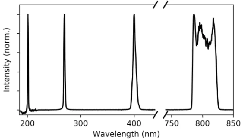
Figure 2.4: Spectrum of the laser fundamental centered at 800 nm, as well as the generated second (400 nm), third (266 nm), and fourth (200 nm) harmonics.
While I will not go into the full details of the setup used here for generating the third and fourth harmonics of our laser (see [49] for the general design reference), I will outline some of the main characteristics it provides. The starting laser is a long cavity oscillator system (Femtolasers XL650) delivering 45 fs pulses with a 4 MHz repetition rate, centered at 800 nm and with a pulse energy of 650 nJ. The generation setup, using an input intensity of about 500 mW (135 nJ) can produce simultaneously the third (266 nm, 4.65 eV) and fourth (200 nm, 6.2 eV) harmonics with typical intensities of about 5 mW and 500 µW, respectively. The spectrum of the harmonics, including the second harmonic and the laser fundamental, are shown in gure 2.4. In terms of photons, these intensities correspond to the order of around 108 photons/pulse (or 1014 photons/s at 4 MHz) for the UV probe pulses. There are some limitations with utilizing this high photon ux in photoemission, however, which I will discuss further in section 2.3. Nevertheless, this provides us with a bright laboratory source of UV photons for use in PEEM and TR-PEEM measurements.
To actually perform a time resolved measurement with fs resolution, as introduced above, a two-pulse scheme is usually needed. Here, I will describe the experimental setup used to achieve this with our system, as shown schematically in gure 2.5. From the laser output, the pulses are rst sent to a pulse compressor, where the dispersion of the ultrafast pulses is compensated for in order to maintain a short pulse duration inside the harmonic generation setup. After the compressor, the beam is split into two paths. One path (probe) is sent to the harmonic generation setup to produce the third and fourth harmonics, which are then directed into the PEEM measurement chamber.
The window on the chamber is made of fused silica in order to prevent absorption of the UV pulses. The other path (pump) is sent to a mechanical delay stage, before entering the measurement chamber, which is used to control the relative arrival time of the pump and probe pulses at the sample with micrometer precision. While gure 2.5 is not to scale, the two path lengths in the experiment must be precisely set in order to achieve overlap of the pulses in time. For reference, in 1 ns light travels a distance of 300 mm (in air), meaning that the two paths must be set to a precision better than 30µm
Figure 2.5: Schematic of the TR-PEEM optical setup used (not to scale). The output of a long cavity titanium sapphire oscillator (Femtolasers XL650) is sent to an external pulse compressor (Swamp Optics BOA-8), before being split into pump and probe paths at a polarized beam splitter, where half wave plates (λ/2) are used to change the ratio of power sent to each path through the beam splitter. The pump is sent (*through an optional BBO and band pass (BP) lter for second harmonic generation, dashed box) to a mechanical delay stage before being sent into the PEEM measurement chamber.
The probe path goes to a home-built third and fourth harmonic generation stage. The desired harmonic is selected with dichroic mirrors for specic wavelengths and movable ipping mirrors before being sent into the PEEM chamber. The measurement chamber has a thin fused silica window in order to prevent absorption of the UV probes. The pump and probe beams hit the sample at a grazing angle of about 17 degrees, and a second window on the opposite side of the chamber allows for viewing any reected laser light on appropriate IR or UV viewing cards.
2.2 Time-resolved photoemission electron microscopy 21 with the delay stage in order to overlap two 100 fs pulses. For specic measurements, the pump photon energy can also be doubled to 3.1 eV (400 nm) through addition of a BBO crystal and band pass lter into the pump path, allowing for excitation of wider band gap materials. Based on the incident angle and distance between the chamber window and sample, the smallest beam size typically achieved (using 1 inch diameter optics with a 250 mm focal length lens) is about 70 µm by 235 µm full width half max (FWHM) of the short and long axis of the elliptical spot, respectively. For these experiments, we use this size for the pump beam, which with the available laser power, allows for excitation uences ranging from a few 10s of nJ/cm2 to around 1 mJ/cm2 per pulse. For the probe, the beam size is sometimes increased to provide more uniform imaging over large areas, however there are also benets to using a more focused beam for high magnication imaging, which can help to reduce space charge, as discussed in section 2.3.1. The overall temporal resolution of our setup, limited by the temporal width of the pump and probe pulses, is around 300 fs at the sample, likely due to dispersion which broadens the probe pulse in the generation setup.
Historically, following the necessary development of modern ultrafast laser sources and PEEM technology, TR-PEEM as a eld has only emerged within roughly the last two decades. Some of the earliest successes with the technique were in studying metallic nanostructures and coupling with surface plasmon polaritons, work which still continues today [46, 47, 5059]. A key feature of the success in this area is to use the local eld enhancement due to the metallic structures to greatly enhance the probability of multiphoton absorption processes. This in turn allows TR-PEEM to map out the local electric eld and how light couples to the surface plasmon modes in such structures, making TR-PEEM a powerful tool to study the nanoscale response of plasmonic nanostructures.
Only more recently, however, has TR-PEEM been applied to study semiconducting materials. Fukumoto, et al. have used TR-PEEM to study the free carrier response in gallium arsenide (GaAs) and demonstrated the ability to observe drift of carriers in an applied eld [60, 61]. They have also shown that recombination kinetics at nanoscale defect sites in GaAs can be studied and quantied with this technique [62]. More recently, they have studied the photocarrier lifetimes in twisted multilayer graphene heterostructures [63]. Another group, at Nanyang Technological University Singapore, has also recently applied TR-PEEM to study the heterogeneous carrier dynamics in monolayer WSe2 akes [64]. Previous work done in our group, led by M. K. L. Man, used TR-PEEM to study the transfer of charges in an indium selenide (InSe) het- erostructure with GaAs, where we observed dierent rates of transfer into dierent thicknesses (with dierent band gaps) of InSe [65]. Recently, work in our group led by E. L. Wong studied the eects of bulk to surface carrier transport in doped GaAs due to the surface band bending, and further demonstrated how the resulting vertical and lateral currents can be optically controlled [66]. These few works studying semicon- ductors with TR-PEEM represent the pioneering work and current state of the art for the technique.
2.3 Considerations for TR-PEEM
In this section, as alluded to previously in section 2.2, there are some limitations and considerations which need to be discussed for performing time resolved photoemission experiments. Here, I will focus on three main challenges. First, I will discuss the issue of space charge in PEEM. Second, I will discuss about the noise in our laser setup. Lastly, I will talk about some of the ideas and challenges with TR-PEEM signal interpretation.
2.3.1 Space Charge
One of the most signicant challenges to overcome is the eect of space charge in the PEEM system. Space charge results when multiple photoemitted electrons are closely grouped, such that they interact, eectively randomizing their trajectories and kinetic energies [67]. For photoemission measurements and microscopy, this can result in a severe loss of both spatial information and kinetic energy information, thus it is of utmost importance to minimize its eect. For time resolved measurements specically, this represents a major issue in terms of selecting a suitable photon source. The issue comes from the fact that for a time resolved measurement, using short pulses of light, the photoelectrons emitted by a sample by a single pulse will be grouped very closely in time. This can lead to very severe space charge eects, especially for measurements using high pulse energy [68]. The way to overcome this problem is to reduce the energy per pulse down to a level where on average, less than one photoelectron per pulse is generated. At this limit, assuming a (relatively low) cross section of photoemission of about10−6 e−/photon, this gives a rough limit of106photons/pulse [69, 70]. Compared to the available108 photons/pulse our laser system can deliver for the fourth harmonic, it is immediately evident that we cannot expect to use anything more than a small fraction of the generated power for staying below the space charge limit. Indeed, in both imaging (gure 2.6) and spectroscopic (gure 2.7) measurements with the third and fourth harmonic probes, respectively, we can easily reach the regime where space charge deteriorates the information quality.
This limit on the pulse energy then places a limit on the number of photoelectrons which can be generated over a given time frame. Therefore, to increase the total number of measured events, a laser with a higher repetition rate must be used. This of course brings in further considerations. First and foremost, is that the lifetime of the excited carriers should be shorter compared to the pulse separation time. If the lifetime is longer, there is a possibility of artifacts in the measured signal, such as an oset or altered dynamics, due to the background of excited carriers in the system. Therefore, ideally, the pulse separation should be longer than the carrier lifetime, meaning that the laser will have a lower repetition rate. For example, a 1 MHz pulsed laser has a pulse separation of 1µs, while a 1 kHz laser has a 1 ms pulse separation. This works to contradict the need for a higher rate of counting statistics; therefore, the signal intensity achievable without space charge must be balanced against the carrier lifetime in order to optimize measurements. Unfortunately, titanium sapphire based lasers often do not have much (if any) tunability in repetition rate, though new ber amplier lasers which have emerged on the market in the last few years may soon make this less of an
2.3 Considerations for TR-PEEM 23
Figure 2.6: PEEM images of a perovskite sample using the third harmonic probe (4.65 eV, 266 nm). At higher probe intensity, space charge eects cause image features to blur and broaden.
Figure 2.7: Photoemission spectra of a perovskite sample at dierent fourth harmonic (6.2 eV, 200 nm) probe intensities. a) normalized photoemission spectrum, where broadening in energy due to space charge can be observed at higher powers. b) The corresponding full width at half max (FWHM) of the spectra in (a).
issue. For our experiments, we have chosen to use a laser with a 4 MHz repetition rate, as described in section 2.2, which results in a pulse separation of 250 ns. For many semiconductors, this is reasonable to not cause problems with the carrier lifetime, and still allows for imaging at a fairly quick rate. As a rough estimate, we nd that given the condition of about one electron produced per pulse, at high magnication (close to instrument resolution limit) we can often image with exposure times on the order of a few seconds (without any imaging apertures). This also matches with the order of the pixel size of the camera (roughly 1 megapixel), meaning that we have at least about one event per pixel in order to ll the image intensity.
A second limitation resulting from space charge, as a more general discussion, is that a lower pulse energy (from a high repetition rate laser) will limit the accessible op- tical nonlinearities, specically the nonlinear processes used to generate either the UV probe or the pump pulses. While oscillator lasers can have sucient pulse energies for producing the 3rd and 4th harmonics of the fundamental [49], as mentioned previously, these lasers do not normally allow for the use of optical parametric ampliers, which are used to continuously tune the photon wavelength in the visible and near-infrared range in high pulse energy, low repetition rate systems. This limits oscillator lasers to excitation with either the fundamental wavelength or a harmonic of it, meaning that resonant pumping of carriers can only be achieved through design and choice of the sample. Hence for the studies here, as mentioned before, we can only excite materials with either the 1.55 eV fundamental or the 3.1 eV second harmonic. Considering again the probe, I would just like to mention that for systems with high pulse energies, other nonlinear methods for generating UV light are possible. The most widespread method under development is higher harmonic generation in gasses, which can produce photon energies of several tens of eV, and potentially into the soft X-ray regime [71]. I mention this as a future outlook for TR-PEEM, as with the recent advent of high repetition rate, high pulse energy ber amplier lasers, the ability to use such nonlinear processes for both pump and probe generation in practical imaging experiments should become much more realistic in the near future, if not already possible.
2.3.2 Laser Noise
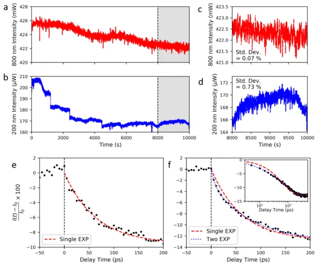
Another important consideration for TR-PEEM measurements is the stability and noise level of the laser system. This is crucial information for designing any experimental plan. Here, I show some basic characterization of the laser setup described earlier in section 2.2. I will rst discuss the intensity stability of the laser and the generated fourth harmonic, shortly after aligning the setup, over a period of several hours as shown in gure 2.8 a and b, respectively. While there is a slow variation in the fundamental intensity, there are sharper changes in the fourth harmonic. This is due to the nonlinear dependence on the intensity and pulse duration, which amplies the small variations in the fundamental. Looking at a time range where the system has stabilized more, (gure 2.8 c, d), I nd that the standard deviation of the fundamental intensity is about 0.07%, which agrees with the laser specication. As expected, the variation is larger in the fourth harmonic intensity, with a standard deviation around 0.73%. Based on this, I expect that TR-PEEM measurements with this system could achieve a sensitivity (percent change in the signal) of around 1% or a little better (particularly for the third
2.3 Considerations for TR-PEEM 25
Figure 2.8: Evaluation of laser stability and noise over time. a) Intensity variation of part of the laser fundamental over several hours. b) Intensity of the generated fourth harmonic over the same time frame as (a). c, d) Zoom-ins of the shaded regions in (a) and (b), with the corresponding standard deviations for this time section of 0.07%
and 0.73% for the fundamental and fourth harmonic (200 nm, 6.2 eV), respectively. e) Representative TR-PEEM signal for a perovskite sample, plotted as the percent change of the signal I(t), relative to the signal without photoexcitation I0 at negative time delay, and t with a single exponential decay (red dashed curve). f) the same data as in (e), but with noise correction by normalization to a reference signal in the PEEM image. In this case, a biexponential t (blue dotted curve) represents the data better than a single exponential (red curve). The inset shows the data on a log scale in delay time, to better emphasize the tting dierences at short time delays.
harmonic probe). From my measurements on perovskite materials, I nd this estimate agrees fairly well. For the representative TR-PEEM curve shown in gure 2.8 e (the measurement details to be discussed in chapter 5), I nd that the standard deviation of the background signal (at negative time delay) is about 0.50% for the third harmonic probe.
While multiple scans and longer averaging are the usual ways to push to better signal to noise, the wide eld imaging achieved in PEEM oers a clever method to reduce the laser noise for TR-PEEM measurements. As mentioned previously in section 1.3, on our perovskite samples we used gold markers as position references (as seen in gure 1.4). Under our experimental conditions, these markers do not show a transient TR-PEEM signal, which allows us to use the photoemission intensity of the marker as an internal reference of the probe intensity (versus externally measuring the power throughout the experiment, for example). Therefore, we can normalize the signal from the sample of interest by the intensity of the gold marker located in the same image in order to reduce intensity uctuations due to the probe. This is shown in gure 2.8 f, which is the same data set shown in gure 2.8 e, but normalized to the intensity of the gold marker in the image. This reduces the standard deviation of the background signal to around 0.28%, almost a factor of two better. The importance of improved signal to noise also becomes apparent from this measurement. In the uncorrected case a single exponential t can reproduce the measured decay, whereas after noise correction it no longer provides as satisfactory of a t, particularly at short time delays. Therefore, unless stated otherwise, all the TR-PEEM intensity traces presented for perovskite samples in the rest of this thesis will use this correction to further improve the signal to noise. Thus, in order to achieve very high signal to noise in TR-PEEM measurements, care should be taken to account for the intensity uctuations of the laser, which will be amplied greatly by the non-linear processes used for UV probe generation.
2.3.3 Signal Interpretation
As a nal consideration for TR-PEEM, it is useful to discuss a relatively simple example of how the changes in photoemission intensity can be understood in a measurement.
For this example, I show TR-PEEM measurements of a p-type GaAs wafer which was cleaved in-situ to expose a fresh (110) surface. Here, we excite the sample with a uence of about 40µJ/cm2/pulse of 1.55 eV photons, and measure the resulting percent change in photoemission intensity with the third (blue circles) and fourth (violet triangles) harmonic probes, as shown in gure 2.9 a. For the third harmonic probe (4.65 eV), there is a sharp increase in the photoemission intensity at zero time delay, followed by a slow recovery on a ns time scale. For the fourth harmonic probe (6.2 eV), we instead see a sharp decrease in the photoemission intensity, with a similar overall time scale.
This dierence in signal is due primarily to the dierent states that the probes couple to, as outlined in gure 2.9 b. For the third harmonic, the photoemission intensity without the pump is very low, due to the GaAs work function being larger than the photon energy. Upon photoexcitation, a large number of electrons are promoted to the conduction band, from where the probe now has sucient energy to excite them above the vacuum level and cause photoemission. Hence, there is a very large transient increase in the measured population. For the fourth harmonic, the probe possesses