INVITED PAPER
Special Section on Terahertz Waves Coming to the Real WorldRecent Progress and Future Prospect of Photonics-Enabled Terahertz Communications Research
Tadao NAGATSUMA†a),Fellow andGuillermo CARPINTERO††,Nonmember
SUMMARY This paper reviews a recent progress in terahertz wireless communications enabled by photonics technologies. After briefly sum- marizing transceiver configurations with electronics and photonics tech- nologies, photonics-based approaches to achieving over 100-Gbit/s data rates are discussed. Then, some of our updated results on real-time wireless transmission experiments using discrete components are shown at data rates up to 50 Gbit/s. Finally, integration technologies are de- scribed by demonstrating latest advances in integrated optical sources and transmitters.
key words: terahertz, communications, photonics, integration
1. Introduction
The data rate of wireless communications has been increas- ing in order to catch up with that of wired and/or fiber- optic communications. The prospective data rate for wire- less communications in the marketplace will be 100 Gbit/s within 10 years[1], [2]. To enable such data rates, there has been a growing interest in the use of terahertz (THz) waves, whose frequencies range from 100 GHz to 1 THz, for broadband wireless communications[1],[3]–[6]. Partic- ularly, above 275 GHz, there is a possibility to employ ex- tremely large bandwidths for “radio” communications, since these frequency bands have not yet been allocated at spe- cific active services, and standardization efforts have been becoming very active[1],[7].
Figure 1 summarizes experimentally achieved data rates of over 1 Gbit/s by transmission experiments with over-100-GHz carrier frequencies at 100–150 GHz[8]–[14], 200–250 GHz[15]–[21], 300–350 GHz[22]–[31], 400–
450 GHz[23], [32], 500–700 GHz[27], [33]–[35]. Data points with triangles are demonstrations using electronics- based transmitter, while data points with circles are achieved by photonics-based ones. Filled and open marks denote data measured with a real-time transmission experiment, and with an off-line signal processing, respectively. The electronics-based approach now enables most of the 100- 150-GHz band wireless links. From 200 GHz to 400 GHz, the photonics-based approach is pushing the front of re- search with respect to the data rate. Above 500 GHz, the data rate still stays low, due mainly to the lack of power
Manuscript received July 15, 2015.
Manuscript revised August 24, 2015.
†The author is with Osaka University, Toyonaka-shi, 560–8531 Japan.
††The author is with University Carlos III of Madrid, Leganes, Madrid, 28911, Spain.
a) E-mail: [email protected] DOI: 10.1587/transele.E98.C.1060
Fig. 1 Data rate vs. carrier frequency obtained for wireless link systems with real-time transmission (filled circle/triangular) and with off-line digital signal processing (open circle/triangular).
emitted from the transmitter.
In this paper, Sect. 2 starts by providing an overview of building blocks of transmitters and receivers for THz com- munications. In the following section, we show our recent system demonstrations using discrete components such as frequency-tunable lasers, optical modulators, photodiodes as well as diode detectors and mixers. Finally, in Sect. 4, we discuss the advances that have been reported using photonic integration technologies to make the system more compact, cost-effective and energy-efficient.
2. Building Blocks
2.1 Transmitters and Receivers
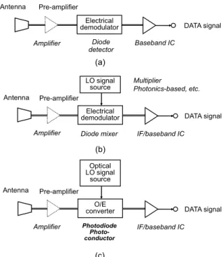
Figures 2 and 3 show schematic diagrams of a transmit- ter and a receiver, respectively. THz communications re- search was initiated with use of photonic techniques for sig- nal generation and modulation as shown in building blocks of the photonics-based transmitter of Fig. 2 (b). Comparing to the all-electronic transmitter of Fig. 2 (a), it has proven to be effective to achieve spurious-free carrier signals[36]and higher data rates of over 20 Gbit/s. This could be realized thanks to the availability of telecom-based high-frequency components such as lasers, modulators and photodiodes (O- E converters). The use of optical fiber cables enables us to distribute high-frequency RF signals over long distances, and makes the size of transmitter frontends compact and light. Moreover, ultimate advantage of the photonics-based Copyright c2015 The Institute of Electronics, Information and Communication Engineers
Fig. 2 Configuration of transmitters based on electronics (a) and pho- tonics (b). RTD: resonant tunneling diode, EOM: electro-optic modulator, EAM: electro-absorption modulator, EDFA: Erbium-doped fiber amplifier, SOA: semiconductor optical amplifier.
Fig. 3 Configuration of receivers based on electronics (a) (b), and pho- tonics (c). As for local oscillator (LO) sources, both electronic and photonic sources can be used.
approach is that wired (fiber-optic) and wireless communi- cation networks could be connected seamlessly in terms of data rates and modulation formats.
As for receivers, all electronic approaches of Figs. 3 (a) and (b) have usually been adopted even with the photonics- based transmitter. The photonics-based receiver has also been reported by using a photodiode as a photonic downconverter[37],[38](Fig. 3 (c)).
As we have seen in the development of 120-GHz- band wireless links, the photonics-based transmitters have been replaced with all-electronic ones. Here, we briefly describe a recent progress of electronic devices and
Fig. 4 Schemes for generation of optical signals with THz frequencies.
DC: direct current source, RF: radio frequency signal source.
circuits. At frequencies above 100 GHz, GaAs and InP devices and integrated circuits (ICs) have been key play- ers in all-electronic THz communications research, because of high cut-offand maximum frequencies of transistors[8]–
[10],[18],[20],[33],[39],[40].
Si-device technologies have started to reveal their po- tential in these 2-3 years[11], [12], [41], [42]. A power combining technique using integrated array antennas has proven to be effective to increase an output power in Si- CMOS transmitter ICs[43],[44]. According to the ITRS roadmap, the half pitch of the wiring in Si-LSIs is expected to become 10∼12 nm by 2020, enabling the maximum op- eration frequency of the mass-production level of Si-CMOS devices reach 1 THz, as well as various RF ICs in excess of 300-GHz operation could be realized in Si-CMOS. GaN and InP ICs, however, have the ability to significantly sur- pass Si devices in terms of the break-down voltage, and are indispensable in applications where a high output power is required. Ultimate terahertz ICs would be a fusion of com- pound semiconductor and Si semiconductor ICs.
Moreover, unique THz electronic devices utilizing the plasma-wave effect in field-effect transistors[45]–[47]and the resonant tunneling effect[30],[33],[48],[49]have at- tracted much interest, because they can be operated as both transmitters and receivers.
2.2 Optical Signal Generators
In the photonics-based system, the optical signal generator, whose intensity is modulated at THz frequencies, is one of the key building blocks as shown in Fig. 4.
Most common optical continuous wave (CW) sig- nal generator with THz frequencies is based on an opti- cal heterodyning, using a dual wavelength optical source.
In this technique, two optical wavelengths λ1 and λ2 are mixed on a photodiode or a photoconductor to generate an electrical beat note with its frequency being determined by the difference of the two optical wavelengths, fbeat = c|λ1 −λ2|/(λ1 ·λ2). There are different solutions to im- plement the dual wavelength source. The most straightfor- ward source involves combining the light from two different
single-frequency semiconductor lasers (Fig. 4 (a)). While its main advantage is the broad tuning range of frequency, the weakness is that the frequency stability is generally poor, requiring locking techniques for the two optical wavelengths[50].
One way to achieve stable signals is to use an exter- nal optical modulator driven by an electronic RF source (Fig. 4 (b)). When an optical intensity modulator is used af- ter a CW single-frequency semiconductor laser, side-bands around the optical wavelength is generated, being spaced by the modulation frequency applied to the modulator. By adequately selecting the modulator operating point, double- sideband suppressed carrier (DSB-SC) generation can be achieved. This suppresses the central optical carrier, leaving the sidebands separated by twice the modulation frequency.
Higher order harmonics can be achieved cascading modula- tors[51]. In this case, optical filters such as arrayed wave- guide gratings (AWGs) and other tunable filters should be used to select only two of harmonic components showing optical frequency comb signals (Fig. 4 (c)).
Another optical CW signal generator with THz fre- quencies is based on optical pulsed sources. The output of the semiconductor laser is a continuous stream of pulses, spaced in time by the inverse of the repetition frequency, frep = c/2ngL, where ng is a refractive index of the laser active layer, and L is a cavity length of the laser. The opti- cal spectrum is a comb of modes, spaced by this frequency.
The main characteristic is that each of the modes is locked in phase to the adjacent ones. In the THz signal generation, the repetition frequency determines the fundamental frequency of THz signals when the pulse train is fed to the O-E con- verter. Higher harmonics can also be used when optical fil- ters are placed before the O-E converter.
There are two types of semiconductor sources that can generate pulses. One is a passively mode-locked (PML) laser diode, where a saturable absorber (SA) section is in- tegrated in the semiconductor laser to lock the phase of each mode (Fig. 4 (d)). This technique produces an optical pulse train only with a DC bias supply, which relaxes an electrical bandwidth requirement significantly. Passive colliding pulse mode-locked (CPM) laser structures enable optical multi- plication of the repetition rate at frequencies from 40 GHz to 500 GHz[51]. The frequency stability improves as the length of the SA reduces. The other is a hybrid mode-locked (HML) laser diode (Fig. 4 (e)). Main feature of this scheme is that the SA section is electrically modulated, allowing a synchronization between the stream of optical pulses and the system clock. It also reduces the timing jitter, just trans- ferring the phase noise characteristics of the RF oscillator to the pulse train[53].
The most straightforward approach to implement these signal generation schemes is to assemble the required dis- crete components. However, the optical fiber connec- tions that are required introduce many problems, including path length variations due to thermal variations. A novel approach, that is becoming readily available nowadays, is to use photonic integration techniques[54]. Photonic
integration allows placing all of the required components onto a single chip. This has several advantages, starting from eliminating fiber coupling losses among the different components. Details will be discussed in Sect. 4.
3. Discrete Systems and Demonstrations
3.1 Direct Detection System
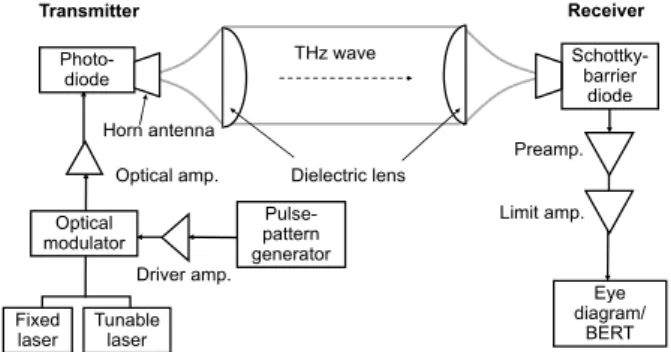
Figure 5 shows a block diagram of the experimental set up to evaluate the wireless link based on intensity modulation and direct detection scheme using the transmitter building block scheme on Fig. 2 (b) with the optical signal source on Fig. 4 (a) and receiver based on Fig. 3 (a). The beat note of optical signals is generated by two free-running lasers with a wavelength difference of 2 nm to be converted to THz waves at 330 GHz by the photodiode. For the mod- ulation, an electro-optic intensity modulator (EOM) driven by electrical data signals from a pulse-pattern-generator is used to perform an amplitude-shift-keying (ASK) modula- tion up to 50 Gbit/s. The modulated optical signal is am- plified by an Er-doped fiber amplifier (EDFA), and finally fed to the waveguide-mounted uni-travelling-carrier (UTC) photodiode[55].
THz waves radiated from the horn antenna (25-dBi gain) are collimated by a dielectric lens (2-inch diameter) in the transmitter. Propagated THz waves are focused by another lens to the horn antenna of the receiver. The to- tal antenna gain is about 40 dBi. The distance between the transmitter and receiver is 0.5 ∼1 m, where there is little change in the received power and a multi-path effect is neg- ligible in the experiment.
The data signal is demodulated by a Schottky-barrier diode (SBD) detector which is mounted on a WR-2.8 wave- guide structure. A 3-dB baseband bandwidth of the detec- tor is 37 GHz. The responsivity of the SBD detector is 2000 V/W. The SBD detector works based on a square-law detection up to the input power level of 100μW. The output baseband signal is amplified by a 38-GHz pre-amplifier and reshaped by a 35-GHz trans-impedance amplifier used as a limiting amplifier.
Figures 6 shows a bit error rate (BER) characteristic of the link and an eye diagram of the demodulated signal in the receiver at 50 Gbit/s. Error-free (BER < 10−11) has been
Fig. 5 Schematic diagram of ASK modulation and direct detection link.
Fig. 6 Bit error rate characteristic and demodulated eye diagram of ASK modulation and direct detection link at a bit rate of 50 Gbit/s with a carrier of 330 GHz.
Fig. 7 (a) Block diagram of the coherent link system. (b) Frequency- and phase-stabilized optical signal generator.
confirmed at a transmitter photocurrent of 6.7 mA, which corresponds to the transmitted power of 90μW. This bit rate might be the highest achievable when we consider band- widths of all the electronic components such as amplifiers including our BER test equipment. By using a polarization multiplexing scheme with wire-grid polarizers, it is possible to double the bit rate to 100 Gbit/s[27].
3.2 Coherent Systems
With RF amplifier-less systems, the coherent link is effective to increase a sensitivity of the receiver, which enables an extension of transmission distance.
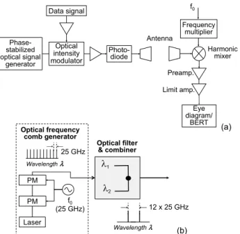
In the transmitter, the carrier frequency and phase are stabilized with a configuration of Fig. 4 (c), while the re- ceiver configuration is based on that of Fig. 3 (b) with a sub- harmonic diode mixer driven by the local oscillator signal with a half frequency of the carrier. Figure 7 shows a de- tailed block diagram of the coherent link system. As for
Fig. 8 Configuration and photo of 20-m distance experiment.
Fig. 9 BER characteristics and an eye diagram showing real-time error- free transmission at 30 Gbit/s at 20-m link distance.
the optical frequency comb generation, we used two electro- optic phase modulators (PM) driven by 25-GHz sinusoidal signals to generate sidebands of over 400-GHz width. We also optimized the amplitude and phase of 25-GHz sig- nals applied to each modulator to maximize the intensity of
“two” optical carriers separated at 300 GHz (12x25 GHz).
By using a programmable optical filter and combiner based on the Liquid Crystal on Silicon (LCoS) technology, we se- lected and combined the two optical carriers. The coherent detection receiver using the SBD mixer has an overall 3- dB baseband bandwidth of 38 GHz. The sensitivity of the coherent detector is typically 20 dB higher than that of the direct detector, although the total receiver sensitivity is de- pendent on RF and baseband bandwidths for the designated data rate.
We performed a 20-m distance transmission experi- ment using the coherent system. In the transmission ex- periment, THz beams radiated from the horn antenna are collimated by aspheric dielectric lenses (100-mm diameter) over the link distance of 20 meters. Simulated gain of such a lens antenna structure is 50 dBi. To perform a proper bit-error-rate (BER) testing enabling the clock synchroniza- tion between the pulse pattern generator and the BER tester, we constructed a round-trip link configuration as shown in Fig. 8.
Figure 9 shows a BER characteristic and eye diagrams at bit rates of 30, 40, and 50 Gbit/s and a link distance of 20 meters. Error-free (BER<10−11) performance was con- firmed at 30 Gbit/s for the photocurrent of∼7 mA, which
corresponds to∼100-μW output power of the transmitter, while error-floors were observed at 40 Gbit/s and 50 Gbit/s.
There are several reasons for this limitation. The most significant one is considered to be a decrease in the received power. The second one is caused by the mismatch of cen- ter frequency of the transmitter and receiver, where the out- put power and sensitivity, respectively, become maximum.
We believe that better performance with respect to the BER characteristics should be obtained by solving these issues.
Currently, we are developing the coherent system with other modulation format like QPSK to increase the data rate up to 100 Gbit/s, and the massive arrays of photodiode to increase the link distance by enhancing the output power of the transmitter up to 10 mW.
4. Photonic Integration Technologies
4.1 Integration Platforms
A Photonic Integrated Circuit (PIC) is a chip that has more than two functional blocks connected through an optical waveguide. The functional building blocks that are required for photonic-based terahertz communications are a photonic signal source, a data modulation, and an optoelectronic converter.
These building blocks can be realized using differ- ent integration technologies, having equivalent functional- ity. One key technological decision is the material sys- tem to use, being Group III-V materials and the Group IV materials the most relevant ones[54]. The first group is mainly represented by Indium Phosphide (InP), while the second group involves all the varieties of Silicon, from Sili- con on Insulator (SOI), Silica on Silicon (SiO2/Si) or Silicon Nitride (Si3N4/SiO2), which are broadly known as Silicon Photonics.
III-V materials have a direct band gap, enabling ac- tive waveguide sections at which optical gain is produced under current injection. This is a key characteristic to de- velop efficient semiconductor lasers. In addition, this ma- terial has different quaternary alloys that provide a wide range of optical characteristics. This enables offering also transparent optical waveguides on InGaAsP for optical in- terconnects and other basic functional components such as multimode interference (MMI) couplers or arrayed wave- guide gratings (AWG). Active-passive photonic integration involves the development of optical junctions between ac- tive and passive waveguide sections. The different layer structure between the active and the passive waveguides in- troduces coupling losses (usually<0.1 dB/junction) as well as back-reflections (<−40 dB).
The possibility to combine active and passive sections on InP allows this material to offer monolithic integration, in which all the components are integrated on the same chip, without joints of seams. Monolithic integration pro- vides lower final cost due to less assembly and testing, smaller size, higher reliability, and enhanced performance.
The most serious drawbacks are the significant performance
trade-offs that are required among the different compo- nents, as well as the back-reflections at the active-passive transitions.
Si-based integration platforms main drawback is that these do not have a direct bandgap, and therefore do not emit light efficiently. Silicon platforms allow integrating passive components only. One of its key advantages is the mechani- cal strength, which has enabled using wafer diameters above 300-mm to increase the yield and reduce the cost. The other is that Silicon has a high-quality native oxide with extremely low optical propagation losses (< 0.003 dB/cm). In addi- tion, being Silicon the integration material for electronics, it is being tackled the issue of using Silicon as common plat- forms for photonics and electronics.
Recently, a radical step forward has been achieved in photonic integration establishing generic integration plat- forms[56], in an effort to make photonics systems cheaper and ubiquitous, providing Multi-Project Wafer (MPW) runs, sharing the fabrication costs among several users.
4.2 Integrated Laser Sources
In this section we present different monolithically integrated semiconductor laser structures specifically designed to serve as an optical signal source implementing a photonic signal millimeter and Terahertz wave generation scheme. As this requires a semiconductor laser, most of the solutions corre- spond to PICs based on InP material system.
Optical heterodyne sources most common approach has been to integrate two lasers on the same substrate and combine their outputs, following the same scheme used with discrete lasers. The key component for this approach is the integrated tunable semiconductor laser, on which effort has been invested for their interest in Wavelength Division Mul- tiplexed optical networks[57], which can be implemented either through a Distributed Feedback (DFB) or Distributed Bragg Reflector (DBR) lasers. The advantage of photonic integrations is that it allows a wide range of component ar- rangements.
One reported solution has been to place the two lasers in axial configuration, including an optical phase modula- tor which is monolithically sandwiched between two DFB lasers. While this extremely compact solution features a continuous tuning range of more than 1 THz, the fact that the lasers have to pass each other to combine the two wave- lengths limits the minimum spacing (and consequently, the lower frequency that can be generated). The minimum sep- aration is determined by the stop bandwidth of the grat- ing[58]. However, the bidirectional operation allows on- chip THz phase control via the optical phase modulator.
A more standard approach, shown in Fig. 10, is to inte- grate the two lasers next to each other, using monolithic pas- sive optical components to combine the two wavelengths.
The monolithic integration of two DFB lasers and an op- tical combiner has been a common solution, either with a Y-junction[59], [60] or MMI coupler. An important de- tail of such integrated schemes is that a reduction in the
free-running beat-note linewidth can be achieved increas- ing the length of the lasers[61]. It has been demonstrated that devices with 2500 μm cavity length exhibit a mini- mum full-width half maximum (FWHM) linewidth of less than 300 kHz, which was sufficient to establish a 1 Gbit/s ASK data transmission wireless link with the two wave- lengths in a free-running state generating a 146-GHz carrier wave[14]. In these structures, the injection current produces a wavelength shift which is often used to tune the generated frequency.
This however creates an asymmetry in the optical power of each mode that increases as the required wave- length difference increases, as both wavelengths shift in the same direction.
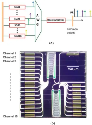
A recent alternative that has been demonstrated makes use of a multi-wavelength laser structure based on an AWG laser which can be fabricated on a generic integration plat- form[62]. The device structure, shown in Fig. 11 (a) is an extended cavity laser, while Fig. 11 (b) shows a realization within a generic foundry. An array of semiconductor opti- cal amplifier (SOA) is multiplexed into a single waveguide through the AWG. The AWG acts as an intra-cavity filter, to establish the lasing wavelengths filtering the modes in the laser cavity formed between the cleaved facets at the end of the channel waveguide on one side and the common wave- guide on the other. The AWG selects a different wavelength for each AWG channel, and combines them on the common waveguide. The wavelength spacing among adjacent chan- nels is determined by the AWG channel spacin, Δλ, typi- cally around 0.8 nm (100 GHz). While the drawback of this approach is that it is difficult to tune the generated wave- lengths, these are extremely narrow producing highly stable frequencies[63].
Regarding pulse sources, there have been two main approaches to integrate mode-locked (ML) semiconductor lasers on a single chip. The first one has been to use ring resonators, providing lithographic control of the cavity length[64]. The main drawback is that ring structures sup- port two counter-propagating modes that compete for the gain, producing instabilities. This requires special design features such as s-shape structures to suppress one propa- gation direction[65]. The second approach uses a cleaved facet on one end of the cavity and a surface-etched grat- ing on the other, with simpler fabrication process than a DBR[66].
Two new types of mirrors, shown in Fig. 12, avoid
Fig. 11 Multi-wavelength arrayed waveguide grating laser. (a) Sche- matic of a 16-channel, showing the multiplexing/filtering function of the AWG. (b) Microscope photograph of cleaved facet structure 16-channels AWGL.
Fig. 12 On-chip mirror alternatives. (a) Sagnac loop. (b) Multimode Interference Reflector.
the need to use the cleaved facets at the chip edge, en- abling on-chip cavity resonators. One option, shown in Fig. 12 (a), is to use Sagnac Loop Reflectors (SLRs). This solution employs an MMI coupler in which two of its out- puts are connected to each other with a loop waveguide[67].
An alternative approach, shown in Fig. 12 (b) employs multi-mode interference reflectors (MIRs). These are an
Fig. 13 On-chip passive mode locked (PML) semiconductor laser.
alternative version in which the MMI is modified to pro- vide an on-chip compact mirror structure that employs total internal reflection from a deep etch facet[68].
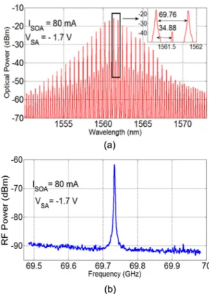
Using this type of mirrors it is possible to build an on- chip PML semiconductor laser. The extremely important advantage of this approach is that we gain lithographic con- trol the cavity length, which in turn determines the repeti- tion rate frequency, eliminating the uncertainty in the cavity length introduced by at the facet cleaving process. In addi- tion, we also achieve full control on the positioning of the SA section within the cavity. Moving the SA away from the mirrors, we achieve multiplying the repetition rate fre- quency by increasing the number of pulses in the cavity. In the top and bottom devices shown in Fig. 13, the SA was lo- cated at the center of the resonator. This allows the cavity to support two counter-propagating pulses that meet at the SA, reducing the energy required per pulse to saturate the ab- sorber. The structure thus is known as colliding pulse mode- locked (CPM), and the repetition rate multiplies by the num- ber of pulses. In the devices shown in Fig. 13, the top one, with cavity length Lcav = 2210μm, aimed to a fundamen- tal repetition rate of 18 GHz. As the SA is located at the center, the repetition rate doubles, achieving 36 GHz. This demonstrated the colliding behavior at a frequency within the range of our Electrical Spectrum Analyzer. The device at the center was a standard Fabry-Perot laser for compari- son, with the same length as the device at the bottom, which was designed to reach the millimeter wave range, employ- ing a shorter cavity, Lcav=1234μm. This sets a fundamen- tal mode spacing of 34 GHz, while the colliding structure allows generating a repetition rate of 69.76 GHz. This is shown in Fig. 14, both on the optical mode spacing as mea- sured using an Optical Spectrum Analyzer, as well as the electrical signal generated coupling the optical output from the laser to a photodiode (U2T XPDV4120R) with 90-GHz (3-dB) bandwidth, connected to an external mixer to down- convert the signal. Locating the SA asymmetrically in the resonator is expected to increase the repetition rate into the THz range.
4.3 Integrated Transmitters
Within the previous section, we describe different semi- conductor laser structures, which can be integrated on a PIC, that implement a photonic-based millimeter- or tera- hertz wave signal generation source. However, dedicated fabrication platforms allow a significant increase in the
Fig. 14 On-chip colliding pulse results when bias at ISOA=80 mA and VSA =−1,7 V. (a) Optical spectrum, the inset shows the frequency mode spacing of 69.76 GHz. (b) Electrical spectrum of the OC-CPML.
Fig. 15 Monolithic integrated transmitter. (a) Mounted chip photograph.
(b) Schematic of the integrated elements in the chip.
functionality offered in a single chip.
A demonstration that has established the state-of-the- art was achieved within the iPHOS (integrated Photonic Sig- nal Sources) project, funded by the European Commission.
The level of integration was raised to the point of achiev- ing a full millimeter-wave wireless transmitter in a single- chip, shown in Fig. 15 (a). As shown in the block diagram in Fig. 15 (b), the chip includes two single mode DFB lasers
previously[69].
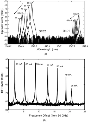
With such structure, we have achieved a wide continu- ous tuning range of the wavelength spacing, over 20 GHz, on different frequency ranges that depend on the initial grat- ing difference. For the device reported, Fig. 16 (a) shows the change in the optical spectrum as the bias current on DFB1 is fixed at 75 mA while the current on DFB2 is varied be- tween 90 mA to 40 mA. When the currents on the two lasers are close to each other (70 mA), the generated beat signal is given by the offset among the grating on each device. As the currents are varied, we can tune the generated frequency.
Increasing the current shifts the wavelength towards longer wavelengths, which as shown in Fig. 16 (a) is used to reduce the spacing, while a decrease in the current shifts the wave- length in the opposite direction. This is an indication that the
Fig. 16 Monolithically integrated dual DFB results varying the current into one DFB2 (90 mA to 36 mA) for a fixed current on DFB1 (75 mA).
(a) Optical Spectrum. (b) Beat signal on an electrical spectrum.
not compensate for the current level difference on the DFBs.
The beat note that is generated on the integrated photodiode, biased at−2.5 V, for each of the different optical spectrums shown previously, is presented in Fig. 16 (b). For the mea- surement we used an F-band sub-harmonic mixer, with a LO frequency of 45 GHz, thus the x-axis represents an offset fre- quency to which must be added 2 x 45 GHz=90 GHz. The tuning range achieved goes from 92 GHz to 110 GHz.
One of the main drawbacks which we have mentioned for optical heterodyne sources that use two different emitters is that the wavelengths are not correlated, and therefore have an excess phase noise. Integrated sources based on DFB lasers have been demonstrated in wireless links at low data rates (100 Mb/s) without any locking scheme[69]. How- ever, in order to reach higher data rates, some phase locking technique must be used. One important advantage of DFB laser structures that include a wavelength selective optical filtering structure within the active region of each emitter is a phase locking when an external optical frequency comb is injected directly into both emitters. Optical injection lock- ing the integrated lasers produces high-spectral-purity sig- nals at frequencies >100 GHz, with phase noise spectral density below−90 dBc/Hz at offsets from the carrier greater than 10 kHz[70]. This is sufficiently stable to achieve a bit-error rate below 10−11 in a 10-Gbit/s coherent wireless transmission link in the W-band (97 GHz carrier frequency) without active phase stabilization on the transmitter side and digital signal processing[71].
5. Conclusion
In this paper, we have reviewed recent progress in THz com- munications technologies enabled by photonics. Photonic generation of high-frequency carrier waves provides an effi- cient access to the millimeter and terahertz frequency ranges for ultrahigh data-rate wireless communications.
At carrier frequencies from 100 GHz to 200 GHz, electronics-based systems with Si-CMOS as well as III- V semiconductor devices have started playing a key role in place of photonics-based ones. 200-GHz and 300-GHz bands have currently been major research targets to achieve 50-Gbit/s to 100-Gbit/s data rate with both approaches.
We have described a real-time 300-GHz band wireless link at 50-Gbit/s data rate with photonics-based systems as a technology demonstrator. In addition, photonics facilitates the convergence of the wired (optical fiber) and wireless communications.
Recent efforts have demonstrated the implementation of millimeter-wave sources using photonic integrated cir- cuits. Monolithic approaches on InP are very much ad- vanced, integrating all the necessary elements on a single chip. The major drawbacks that we have observed are the highly complex fabrication process flow (three epitaxial re- growth steps), the limited tuning range (around tenths of GHz) and the number of compromises that must be made to monolithically integrate all the components, which limit the performance of photodiodes, and SOAs. In our view, an optimized photonic-electronic convergence will require hy- brid integration approaches, using standardized components as well as assembly and packing solutions.
The photonic integration approach is now at an ex- tremely exciting stage, in which there are multiple options competing among each other. Generic foundry technology platforms will play an important role in providing the low- cost development of the photonics-based THz transceivers.
It will provide tunability/bandwidth of 100 GHz to 1 THz and a data rate of over 100 Gbit/s, which will not be easily achieved by all electronic approaches.
Acknowledgments
We would like to thank Dr. S. Kuwano, Dr. J. Terada of NTT Access Network Systems Laboratories, Prof. S. Hisatake, Mr. K. Oogimoto, Mr. Y. Yasuda, Mr. Y. Inubushi, and Mr.
Y. Fujita of Osaka University, for their technical support and help. We also acknowledge all the partners of the iPHOS (www.iphos-project.eu) for invaluable discussions, and spe- cially Fr´ed´eric Van Dijk, from Alcatel-Lucent III-V LAB, where the fully monolithic chip was processed. Special thanks should be given to University Carlos III of Madrid and Banco de Santander for the Chair of Excellence fund- ing scheme, which has enabled the collaboration between the authors.
This work was supported in part by the 2014/2015 Strategic Information and Communications R&D Promo- tion Programme (SCOPE: 135010103), from the Min- istry of Internal Affairs and Communications, Japan, and by the Spanish Ministerio de Economia y Competitividad DiDACTIC project (TEC2013-47753-C3-3-R) and Conse- jer´ıa de Educaci´on, Juventud y Deporte of Comunidad de Madrid DIFRAGEOS project (P2013/ICE-3004).
References
[1] T. K¨urner and S. Priebe, “Towards THz communications-status in re- search, standardization and regulation,” J. Infrared, Millimeter, and Terahertz Waves, vol.35, issue 1, pp.53–62, 2014.
[2] IWPC Ultra High Capacity Networks White Paper, Evolution- ary & disruptive visions towards ultra high capacity networks,”
http://www.iwpc.org/WhitePapers.aspx#5000x
[3] J. Federici and L. Moeller, “Review of terahertz and subterahertz wireless communications,” J. Appl. Phys., vol.107, no.11, p.111101, 2010.
[4] T. Kleine-Ostmann and T. Nagatsuma, “A review on terahertz com- munications research,” J. Infrared, Millimeter, and Terahertz Waves, vol.32, no.2, pp.143–171, 2011.
[5] H.-J. Song and T. Nagatsuma, “Present and future of terahertz communications,” IEEE Trans. THz Sci. Technol., vol.1, no.1, pp.256–263, 2011.
[6] T. K¨urner, “Towards future THz communications systems,” J. Tera- hertz Science and Technology, vol.5, no.1, pp.11–17, 2012.
[7] http://www.ieee802.org/15/pub/index TG3d.html
[8] A. Hirata, T. Kosugi, H. Takahashi, J. Takeuchi, H. Togo, M. Yaita, N. Kukutsu, K. Aihara, K. Murata, Y. Sato, T. Nagatsuma, and Y. Kado, “120-GHz-band Wireless link Technologies for Outdoor 10-Gbit/s Data Transmission,” IEEE Trans. Microw. Theory Techn., vol.60, no.3, pp.881–895, 2012.
[9] H. Takahashi, A. Hirata, J. Takeuchi, N. Kukutsu, T. Kosugi, and K.
Murata, “120-GHz-band 20-Gbit/s transmitter and receiver MMICs using quadrature phase shift keying,” Proc. 7th European Microwave Integrated Circuits Conference, pp.313–316, 2012.
[10] J. Takeuchi, A. Hirata, H. Takahashi, and N. Kukutsu, “10-Gbit/s bi-directional and 20-Gbit/s uni-directional data transmission over a 120-GHz-band wireless link using a finline ortho-mode transducer,”
Proc. Asia-Pacific Microwave Conf. (APMC 2010), pp.195–198, 2010.
[11] R. Fujimoto, R.M. Motoyoshi, K. Takano, and M. Fujishima, “A 120 GHz/140 GHz dual-channel ASK receiver using standard 65 nm CMOS technology,” Proc. 41st European Microwave Conf. (EuMC 2011), pp.1189–1192, 2011.
[12] M. Fujishima, “Low-power ultrahigh-speed mobile communication with terahertz circuits,” Tech. Dig. IEEE 12th International Con- ference on Solid-State and Integrated Circuit Technology (ICSICT- 2014), O19 03, Beijing, 2014.
[13] C. Wang, C. Lin, Q. Chen, X. Deng, and J. Zhang, “0.14 THz high speed data communication over 1.5 kilometers,” Tech. Dig. of In- frared Millimeter, and Terahertz Waves (IRMMW-THz 2012), paper Tue-A-2-4, 2012.
[14] M.J. Fice, E. Rouvalis, F. van Dijk, A. Accard, F. Lelarge, C.C.
Renaud, G. Carpintero, and A.J. Seeds, “146-GHz millimeter-wave radio-over-fiber photonic wireless transmission system,” Opt. Ex- press., vol.20, no.2, pp.1769–1774, Jan. 2012.
[15] G. Ducournau, P. Szriftgiser, D. Bacquet, A. Beck, T. Akalin, E.
Peytavit, M. Zaknoune, and J.F. Lampin, “Optically power sup- plied Gbit/s wireless hotspot using 1.55μm THz photomixer and heterodyne detection at 200 GHz,” Electron. Lett., vol.46, no.19, pp.1349–1351, 2010.
[16] G. Ducournau, Y. Yoshimizu, S. Hisatake, F. Pavanello, E. Peytavit, M. Zaknoune, T. Nagatsuma, and J.-F. Lampin, “Coherent THz com- munication at 200 GHz using a frequency comb, UTC-PD and elec- tronic detection,” Electron. Lett., vol.50, no.5, pp.386–388, 2014.
[17] A.J. Seeds, H. Shams, M.J. Fice, and C.C. Renaud, “Terahertz pho- tonics for wireless communications,” J. Lightw. Technol., vol.33, no.3, pp.579–587, 2015.
[18] I. Kallfass, J. Antes, T. Schneider, F. Kurz, D. Lopez-Diaz, S.
Diebold, H. Massler, A. Leuther, and A. Tessmann, “All active MMIC-based wireless communication at 220 GHz,” IEEE Trans.
THz Sci. Technol., vol.1, no.2, pp.477–487, 2011.
[19] S. Koenig, D. Lopez-Diaz, J. Antes, F. Boes, R. Henneberger, A.
Leuther, A. Tessmann, R. Schmogrow, D. Hillerkuss, R. Palmer, T. Zwick, C. Koos, W. Freude, O. Ambacher, J. Leuthold, and I.
Kallfass, “Wireless sub-thz communication system with high data rate,” Nat Photon, vol.7, no.12, pp.977–981, Dec. 2013.
[20] F. Boes, T. Messinger, J. Antes, D. Meier, A. Tessmann, A. Inam, and I. Kallfass, “Ultra-broadband MMIC-based wireless link at 240 GHz enabled by 64GS/s DAC,” 2014 39th International Confer- ence on Infrared, Millimeter, and Terahertz waves (IRMMW-THz), pp.1–2, Sept. 2014.
[21] J. Antes, S. Koenig, D. Lopez-Diaz, F. Boes, A. Tessmann, R.
Henneberger, O. Ambacher, T. Zwick, and I. Kallfass, “Transmis- sion of an 8-PSK modulated 30 Gbit/s signal using an MMIC-based 240 GHz wireless link,” Tech. Dig. 2013 IEEE MTT-S International in Microwave Symposium Digest (IMS 2013), pp.1–3, June 2013.
pp.953–954, July 2012.
[25] T. Nagatsuma, “Generating millimeter and terahertz waves by pho- tonics for communications and sensing,” Tech. Dig. IEEE Interna- tional Microwave Symposium (IMS 2013), paper WE2H-1, 2013.
[26] H.-J. Song, J.-Y. Kim, K. Ajito, M. Yaita, and N. Kukutsu, “Fully integrated ASK receiver MMIC for terahertz communications at 300 GHz,” IEEE Trans. THz Sci. Technol., vol.3, no.4, pp.445–452, July 2013.
[27] T. Nagatsuma, S. Horiguchi, Y. Minamikata, Y. Yoshimizu, S.
Hisatake, S. Kuwano, N. Yoshimoto, J. Terada, and H. Takahashi,
“Terahertz wireless communications based on photonics technolo- gies,” Opt. Express, vol.21, no.20, pp.23736–23747, 2013.
[28] T. Nagatsuma, “300-GHz-band wireless communications with high- -power photonic sources,” Proc. 31th URSI General Assembly and Scientific Symposium, DFC01.3, Beijing, 2014.
[29] A. Kanno, I. Morohashi, T. Kuri, I. Hosako, T. Kawanishi, Y.
Yasumura, Y. Yoshida, and K.-I. Kitayama, “16-Gbaud QPSK radio transmission using optical frequency comb with recirculating fre- quency shifter for 300-GHz RoF signal,” Tech. Dig. IEEE Topical Meeting on Microwave Photonics (MWP 2012), pp.298–301, 2012.
[30] T. Nagatsuma, M. Fujita, A. Kaku, D. Tsuji, S. Nakai, K. Tsuruda, and T. Mukai, “Terahertz wireless communications using reso- nant tunneling diodes as transmitters and receivers,” Proc. Intern.
Conf. Telecommunications and Remote Sensing (ICTRS 2014), Luxembourg, 41, 2014.
[31] C. Wang, B. Lu, C. Lin, Q. Chen, L. Miao, X. Deng, and J. Zhang,
“0.34-THz wireless link based on high-order modulation for future wireless local area network applications,” IEEE Trans. THz Sci.
Technol., vol.4, no.1, pp.75–85, 2014.
[32] G. Ducournau, P. Szriftgiser, A. Beck, D. Bacquet, F. Pavanello, E. Peytavit, M. Zaknoune, T. Akalin, and J.-F. Lampin, “Ultra- wide-bandwidth single-channel 0.4-THz wireless link combining broadband quasi-optic photomixer and coherent detection,” IEEE Trans. THz Sci. Technol., vol.4, no.3, pp.328–337, May 2014.
[33] K. Ishigaki, M. Shiraishi, S. Suzuki, M. Asada, N. Nishiyama, and S. Arai, “Direct intensity modulation and wireless data transmission characteristics of terahertz-oscillating resonant tunneling diodes,”
Electron. Lett., vol.48, no.10, pp.582–583, 2012.
[34] L. Moeller, J.F. Federici, and K. Su, “THz wireless communica- tions: 2.5 Gb/s error-free transmission at 625 GHz using a narrow- bandwidth 1 mW THz source,” Tech. Dig. of URSI General Assem- bly and Scientific Symposium, Turkey (URSI GASS 2011), paper DAF2-7.
[35] G. Ducournau, P. Szriftgiser, F. Pavanello, E. Peytavit, M. Zaknoune, D. Bacquet, A. Beck, T. Akalin, and J.-F. Lampin, “THz communi- cations using photonics and electronic devices: the race to data-rate,”
J. Infrared Milli. Terhz. Waves, vol.36, pp.198–218, 2015.
[36] H. Takahashi, A. Hirata, K. Ajito, S. Hisatake, and T. Nagatsuma,
“10-Gbit/s close-proximity wireless system meeting the regulation for extremely low-power radio stations,” IEICE Electron. Express, vol.11, no.3, p.20130989, Jan. 2014.
[37] T. Nagatsuma, A. Kaino, S. Hisatake, K. Ajito, H.-J. Song, A.
Wakatsuki, Y. Muramoto, N. Kukutsu, and Y. Kado, “Continu- ous-wave Terahertz Spectroscopy System Based on Photodiodes,”
PIERS Online, vol.6, no.4, pp.390–394, 2010.
ahertz communications at 300 GHz,” IEEE Trans. Microw. Theory Techn., vol.62, issue 3, pp.600–609, 2014.
[41] J.-D. Park, S. Kang, S.V. Thyagarajan, E. Alon, and A.M. Niknejad,
“A 260 GHz fully integrated CMOS transceiver for wireless chip- to-chip communication,” Proc. IEEE Symposium on VLSI Circuits, pp.48–49, Honolulu, June 2012.
[42] Z. Wang, P.-Y. Chiang, P. Nazari, C.-C. Wang, Z. Chen, and P.
Heydari, “A CMOS 210-GHz fundamental transceiver with OOK modulation,” IEEE J. Solid-State Circuits, vol.49, no.3, pp.564–580, 2014.
[43] K. Sengupta and A. Hajimiri, “A 0.28THz 4×4 power-generation and beam-steering array,” IEEE Intern. Solid-State Circuits Confer- ence (ISSCC2012), pp.256–258, Feb. 2012.
[44] R. Han and E. Afshari, “A 260GHz Broadband Source with 1.1mW Continuous-Wave Radiated Power and EIRP of 15.7dBm in 65nm CMOS,” IEEE Int. Solid-State Circuit Conf. (ISSCC), San Francisco, CA, Feb. 2013.
[45] M.I. Dyakonov, “Generation and detection of Terahertz radiation by field effect transistors,” Compt. Rend. Phys., vol.11, no.7-8, pp.413–420, 2010.
[46] T. Otsuji, T. Watanabe, S.A.B. Tombet, A. Satou, W.M. Knap, V.V.
Popov, M. Ryzhii, and V. Ryzhii, “Emission and detection of ter- ahertz radiation using two-dimensional electrons in III-V semicon- ductors and graphene,” IEEE Trans. THz Sci. Technol., vol.3, issue 1, pp.63–71, Jan. 2013.
[47] S. Blin, L. Tohme, D. Coquillat, S. Horiguchi, Y. Minamikata, S.
Hisatake, P. Nouvel, T. Cohen, A. Penarier, F. Cano, L. Varani, W.
Knap, and T. Nagatsuma, “Wireless communication at 310 GHz us- ing GaAs high-electron-mobility transistors for detection,” J. Com- mun. Netw., vol.15, no.6, pp.559–568, Dec. 2013.
[48] H. Kanaya, H. Shibayama, R. Sogabe, S. Suzuki, and M. Asada,
“Fundamental oscillation up to 1.31 THz in resonant tunneling diodes with thin well and barriers,” Appl. Phys. Express, vol.5, no.12, p.124101, 2012.
[49] T. Shiode, T. Mukai, M. Kawamura, and T. Nagatsuma, “Giga-bit wireless communication at 300 GHz using resonant tunneling diode detector,” Proc. Asia-Pacific Microwave Conference (APMC2011), WE6A-01, pp.1122–1125, Melbourne, 2011.
[50] F. Friederich, G. Schuricht, A. Deninger, F. Lison, G. Spickermann, P.H. Bol´ıvar, and H.G. Roskos, “Phase-locking of the beat signal of two distributed-feedback diode lasers to oscillators working in the MHz to THz range,” Opt. Express, vol.18, no.8, pp.8621–8629, 2010.
[51] Y. Gao, A. Wen, Q. Yu, N. Li, G. Lin, S. Xiang, and L. Shang,
“Microwave generation with photonic frequency sextupling based on cascaded modulators,” IEEE Photon. Technol. Lett., vol.2, no.12, pp.1199–1202, 2014.
[52] S. Arahira and Y. Ogawa, “480-GHz subharmonic synchronous mode locking in a short-cavity colliding-pulse mode-locked laser diode,” IEEE Photon. Technol. Lett., vol.14, no.4, pp.537–539, 2002.
[53] G. Carpintero, M.G. Thompson, R.V. Penty, and I.H. White, “Low noise performance of passively mode-locked 10-GHz quantum-dot laser diode,” IEEE Photon. Technol. Lett., vol.18, no.6, pp.755–757, 2009.
[54] C.R. Doerr, “Integrated photonic platforms for telecomunications:
InP and Si,” IEICE Trans. Electron., vol.E96-C, no.7, pp.950–957, 2013.
[55] T. Nagatsuma, H. Ito, and T. Ishibashi, “High-power RF photo- diodes and their applications,” Laser Photon. Rev., vol.3, no.1-2, pp.123–137, 2009.
[56] M. Smit, X. Leijtens, H. Ambrosius, E. Bente, J.V. Tol, B.
Smalbrugge, T. de Vries, E.-J. Geluk, J. Bolk, R. van Veldhoven, L. Augustin, P. Thijs, D. D’Agostino, H. Rabbani, K. Lawniczuk, S.
Stopinski, S. Tahvili, A. Corradi, E. Kleijn, D. Dzibrou, M. Felicetti, E. Bitincka, V. Moskalenko, J. Zhao, R. Santos, G. Gilardi, W. Yao, K. Williams, P. Stabile, P. Kuindersma, J. Pello, S. Bhat, Y. Jiao, D.
Heiss, G. Roelkens, M. Wale, P. Firth, F. Soares, N. Grote, M. Schell, H. Debregeas, M. Achouche, J.-L. Gentner, A. Bakker, T. Korthorst, D. Gallagher, A. Dabbs, A. Melloni, F. Morichetti, D. Melati, A.
Wonfor, R. Penty, R. Broeke, B. Musk, and D. Robbins, “An in- troduction to InP-based generic integration technology,” Semicond.
Sci. Tech., vol.29, no.8, p.083001, June 2014.
[57] L.A. Coldren, G.A. Fish, Y. Akulova, J.S. Barton, L. Johansson, and C.W. Coldren, “Tunable semiconductor lasers: A tutorial,” J.
Lightw. Technol., vol.22, no.1, pp.193–202, Jan. 2004.
[58] T. G¨obel, D. Stanze, R.J.B. Dietz, H. Roehle, M. Schlak, B.
Sartorius, and M. Schell, “Next generation continuous wave THz systems,” Proc. 36th Int. Conf. Infrared and Millimeter Waves (IRMMW THz), Houston, USA, Oct. 2011.
[59] C. Laperle, M. Svilans, M. Poirier, and M. Tetu, “Frequency multi- plication of microwave signals by sideband optical injection locking using a monolithic dual-wavelength DFB laser device,” IEEE Trans.
Microw. Theory Techn., vol.47, no.7, pp.1219–1224, July 1999.
[60] J. Huang, C. Sun, B. Xiong, and Y. Luo, “Y-branch integrated dual wavelength laser diode for microwave generation by sideband injec- tion locking,” Opt. Express, vol.17, no.23, pp.20727–20734, 2009.
[61] F. van Dijk, A. Accard, A. Enard, O. Drisse, D. Make, and F. Lelarge, “Monolithic dual wavelength DFB lasers for narrow linewidth heterodyne beat-note generation,” Proc. Int. Top. Meet.
Microw. Photon. Jointly held with Asia-Pacific Microw. Photon.
Conf., pp.73–76, Oct. 2011.
[62] K. Lawniczuk, R. Piramidowicz, P. Szczepanski, P.J. Williams, M.J.
Wale, M.K. Smit, and X.J.M. Leijtens, “8-channel AWG-based mul- tiwavelength laser fabricated in a multi-project wafer run,” Proc.
23rd International Conference on Indium Phosphide and Related Materials (IPRM 2011).
[63] G. Carpintero, E. Rouvalis, K. Ławniczuk, M. Fice, C.C. Renaud, X.J.M. Leijtens, E.A.J.M. Bente, M. Chitoui, F. Van Dijk, and A.J.
Seeds, “95 GHz millimeter wave signal generation using an arrayed waveguide grating dual wavelength semiconductor laser,” Opt. Lett., vol.37, no.17, pp.3657–3659, 2012.
[64] J.P. Hohimer and G.A. Vawter, “Passive mode locking of monolithic semiconductor ring lasers at 86 GHz,” Appl. Phys. Lett., vol.63, no.12, pp.1598–1600, 1993.
[65] H. Cao, H. Deng, H. Ling, C. Liu, V.A. Smagley, R.B. Caldwell, G.A. Smolyakov, A.L. Gray, L.F. Lester, P.G. Eliseev, and M.
Osinski, “Unidirectional operation of quantum-dot ring lasers,” Con- ference on Lasers and Electro-Optics, (CLEO), vol.3, pp.1793–1795, 2005.
[66] L. Hou, M. Haji, and J.H. Marsh, “Monolithic Mode-locked laser with an integrated optical amplifier for low-noise and high-power operation,” IEEE J. Sel. Topics Quantum Electron., vol.19, no.4, p.1100808, 2013.
[67] P. Mu˜noz, R. Garc´ıa-Olcina, C. Habib, L.R. Chen, X.J.M. Leijtens, T. de Vries, D. Robbins, and J. Capmany, “Label swapper device for spectral amplitude coded optical packet networks monolithically integrated on InP,” Opt. Express., vol.19, issue 14, pp.13540–13550, 2011.
[68] E. Kleijn, M.K. Smit, and X.J.M. Leijtens, “Multimode interference reflectors: A new class of components for photonic integrated cir- cuits,” J. Lightw. Technol., vol.31, no.18, pp.3055–3063, 2013.
[69] F. van Dijk, G. Kervella, M. Lamponi, M. Chtioui, F. Lelarge, E. Vinet, Y. Robert, M.J. Fice, C.C. Renaud, A. Jimenez, and G.
Carpintero, “Monolithically integrated InP Heterodyne millimeter wave source for high data rate transmission,” IEEE Photon. Tech- nol. Lett., vol.26, no.10, pp.965–968, May 2014.
[70] K. Balakier, M.J. Fice, F. van Dijk, G. Kervella, G. Carpintero, A.J.
Seeds, and C.C. Renaud, “Optical injection locking of monolithi- cally integrated photonic source for generation of high purity signals above 100 GHz,” Opt. Express., vol.22, no.24, pp.29404–29412, 2014.
[71] S. Hisatake, G. Carpintero, Y. Yoshimizu, Y. Minamikata, K.
Oogimoto, Y. Yasuda, F. van Dijk, T. Tekin, and T. Nagatsuma,
“W-Band coherent wireless link using injection-locked laser diodes,” IEEE Photon. Technol. Lett., vol.27, no.14, pp.1565–1568, July 2015.
Tadao Nagatsuma received B.S., M.S., and Ph.D. degrees in electronic engineering from Kyushu University, Fukuoka, Japan, in 1981, 1983, and 1986, respectively. From 1986 to 2007, he was with Nippon Telegraph and Tele- phone Corporation (NTT), Atsugi, Kanagawa, Japan. Since 2007, he has been a Profes- sor at Graduate School of Engineering Science, Osaka University. His research interests in- clude millimeter-wave and terahertz photonics and their application to sensors and wireless communications. He is a Fellow of the IEICE, the Electromagnetics Academy, and the IEEE.
Guillermo Carpintero is Associate Profes- sor at the Electronics Technology Department of Carlos III University of Madrid (UC3M) Earned his engineering degree at Universidad Polit´ecnica de Madrid and his PhD at UC3M.
He has been visiting researcher at the Center for Advanced Photonics and Electronics (CAPE) at University of Cambridge, Visiting Professor at University College London and Osaka Univer- sity. Was awarded the “Heather Williamson Young Investigator Award” in 2000 from the In- ternational Society for Optics and Photonics (SPIE), Award of Excellence Social Council of UC3M in 2009 and the Award for Best European R & D Project in Cooperation MadrI+D Foundation in 2011. He is in the editorial board of the IET Optoelectronics journal.
![Figure 1 summarizes experimentally achieved data rates of over 1 Gbit/s by transmission experiments with over-100-GHz carrier frequencies at 100–150 GHz [8]–[14], 200–250 GHz [15]–[21], 300–350 GHz [22]–[31], 400–](https://thumb-ap.123doks.com/thumbv2/123deta/5625133.1500122/1.892.470.817.293.516/figure-summarizes-experimentally-achieved-transmission-experiments-carrier-frequencies.webp)