Takayuki FUJITA†a),Member
SUMMARY This paper introduces the basics of energy harvesters and demonstrates two specific vibratory-type energy harvesters developed at the University of Hyogo. The fabrication and evaluation results of the vibratory-type energy harvesters, which employ electrostatic and electro- magnetic mechanisms, are described. The aim of developing these devices is to realize a power source for an autonomous human monitoring system.
The results of harvesting from actual human activities obtained using a data logger are also described. Moreover, challenges in the power management of electronic circuitry used for energy harvesting are briefly discussed.
key words: energy harvester, wireless sensor network, WSN, photovoltaic cell, thermo electric generator, RF harvester, electrostatic, electromag- netic, vibratory type
1. Introduction
Wireless-sensor-network (WSN) and body-area-network (BAN) systems, which consist of ultrasmall portable de- vices such as micro-electromechanical systems (MEMS) sensors, a microcontroller unit (MCU), a radio frequency (RF) transceiver and a power source, have attracted consid- erable attention for their use in various applications [1]–[3].
Our group is developing a WSN for a human-monitoring system that continuously monitors human health, including the amount of exercise and vital signs [4]. The system can be divided into four sections: (1) sensing of the human body [5], (2) integrated circuitry, (3) a microscale power source and (4) a data analysis part. The system is expected to have the appearance of a sticking plaster so that it can be used as an attachable system. A total system is installed on the flexible ‘plaster’, as shown in Fig. 1, which is attached di- rectly onto the body. The system gathers many types of data, which are suitably processed and transferred to an external host PC.
The system manages the information obtained from human activities in daily life and the surrounding environ- ment. For such a system, the most important requirement is long-time operation to realize a continuous monitoring system. However, the capability and cost of the system are limited by the finite capacity of power supply. Thus, an energy harvester that can act as an autonomous power source is a promising means of providing supplementary power. To generate energy from the human body and the surrounding environment, photovoltaic cells (PVCs), ther- moelectronic generators (TEGs), ambient RF (electromag-
Manuscript received February 14, 2013.
†The author is with the Graduate School of Engineering, Uni- versity of Hyogo, Himeji-shi, 671-2280 Japan.
a) E-mail: [email protected] DOI: 10.1587/transele.E96.C.766
Fig. 1 Conceptual schematic of human-monitoring plaster.
netic wave) energy harvesters and vibratory energy har- vesters (VEHs) have been widely studied [6]. In this pa- per, the basics of energy harvesters as an autonomous power source for a WSN node are introduced. Then two mecha- nisms of VEH that use an electrostatic (electret type) mech- anism and an electromagnetic mechanism that have been de- veloped at the University of Hyogo are demonstrated. Addi- tionally, the results of harvesting from actual human move- ment using the electret energy harvester with a human ac- tivity logger are also described. Finally, challenges in the power management of circuitry used for energy harvesting are discussed.
2. Wireless Sensor Network and Energy Harvesting Figure 2 shows a typical block diagram of a WSN node con- sisting of a sensor, an analog to digital converter (ADC), MCU, a RF module and a power source. The power con- sumption of the WSN node depends on the number of sens- ing elements and the frequency of data acquisition but it can- not exceed approximately 100µW [7]. To enable the contin- uous operation of the node for a long time, the combination of a rechargeable device and an energy harvester is the most feasible choice.
Energy harvesting, also known as energy scavenging or parasitic power harvesting, has recently attracted consid- erable interest in the WSN research field [8]. It involves the gathering of electric energy from various sources of en- ergy in a range of environments. There are various types of Copyright c2013 The Institute of Electronics, Information and Communication Engineers
Fig. 2 Basic arrangement of wireless sensor network node.
Table 1 Typical characteristics of energy harvesters [6].
Fig. 3 Schematic diagram of dye-sensitized solar cell.
harvesters and sources, such as PVCs, heat (thermal gradi- ent), ambient RF and kinetic (vibration) energies. Table 1 shows typical power sources and performances of energy harvesters [6]. Although the harvested powers are rather low, the power consumption of WSN nodes has drastically decreased in the last decade. Details of each harvesting method are described as follows.
2.1 Photovoltaic Cells (PVCs)
PVCs are considered to be the world’s first and most power- ful energy harvesters, which convert light photons into elec- tricity. The efficiency range is from 5 to 30% for a source power of 100 mW/cm2for outdoor use and 100µW/cm2for indoor use, depending of the material [6]. PVC technologies are well developed and have been well studied. In particu- lar, dye-sensitized solar cells (DSSCs) have attracted atten- tion because of their high efficiency for indoor use through the matching of the dye color to the wavelength of the light source. As shown in Fig. 3, DSSCs are composed of trans- parent electrodes, porous TiO2 for dye adsorption and an electrolyte. Indoor light, particularly LED and fluorescent lighting systems will be the main light source used for har- vesting.
2.2 Thermoelectric Generators (TEGs)
TEGs harvest energy by using the Seebeck effect, in which
Fig. 5 Schematic diagram of RF harvester with rectenna.
voltage is generated from different conductors with differ- ent temperatures. Figure 4 shows the basic principle of a TEG. When p-type and n-type semiconductors are con- nected in series and a thermal gradient is applied in parallel, thermopower is generated. Each pair forms a thermocou- ple. Bi2Te3 is the most commonly used material in TEGs since it allows them to operate near room temperature. The thermopower increases with the square of the Seebeck co- efficient and with the electric conductivity and decreases in- versely with the thermal conductivity. To obtain a high volt- age, some commercially available TEGs have a large num- bers of thermocouples connected in series. The thermocou- ples also have a thermal parallel connection so that a thermal gradient can be applied. TEG 540 thermocouples connected in series over a 3.3×3.3 mm2area can generate a power of 140 mV/K [9].
2.3 Ambient RF Harvesters
Ambient radio waves from TV broadcasting, Wi-Fi net- works and GSM mobile phone systems can be considered as energy sources for RF energy harvesters because they can be captured everywhere and have sufficient power for WSN. Figure 5 shows a typical RF harvester that consists of an antenna and a rectifier. This combination is called a rectenna, the role of which is to convert from AC volt- age to DC voltage. The received power strongly depends on the distance from the power source. For example, power of 1.5 mW and 200µW are received from a 100 mW transmis- sion power source at distance of 0.2 and 2 m, respectively [10].
2.4 Vibratory Energy Harvesters (VEHs)
There are various mechanisms for converting from the mo- tion or vibration to electrical energy. Figure 6 shows the principles of (a) piezoelectric, (b) electrostatic and (c) elec- tromagnetic VEHs. A piezoelectric harvester generates charge by applying stress (Fig. 6(a)), an electrostatic har- vester induces the movement of charges (i.e., current) on
Fig. 6 Principles of VEHs using (a) piezoelectric, (b) electrostatic and (c) electromagnetic mechanisms.
an electret by electrostatic induction (Fig. 6(b)) and an elec- tromagnetic harvester generates an electromotive force by changing the magnetic flux near a pickup coil (Fig. 6(c)).
The harvesting energy is proportional to the mass under- going vibration, the vibration frequency and the vibration amplitude. Therefore, to obtain a large amplitude at the resonance frequency, the resonant vibration harvester is the most widely studied VEH. However, it is difficult to obtain a vibrating structure with low frequency and large amplitude simultaneously since these factors have a trade-offrelation- ship. Similarly to an RF harvester, a VEH generates an AC output, meaning that an AC to DC converter or rectifying circuitry is required.
3. Vibratory Energy Harvesters for Human-Monitoring Systems
The advantages and disadvantages of each type of harvest- ing method are discussed in [10]. We considered the VEH to be the most suitable harvester for human-monitoring appli- cations. Below we report two types of harvester that we are developing in our current project. Additionally, preliminary evaluation results for the harvesting of energy from human activities are also given.
3.1 Electrostatic VEH
In VEHs, an electrostatic mechanism that uses an electret has been reported to be suitable for generating power in the case of low-frequency vibration as the source, such as hu- man motion. This is because an electret in a VEH can gen- erate a high voltage even in the case of low-frequency vi- bration. Our VEH containing an electret has a three-layered silicon MEMS structure as shown in Fig. 7 [11]. Figure 8 shows a schematic diagram of the cross section of the elec- tret VEH. The top layer is a silicon counter electrode con-
Fig. 7 Schematic diagram of electret VEH ( c2011, IEEE [11]).
Fig. 8 Schematic of cross section of the electret VEH ( c2010, Elsevier [13]).
taining multiple slits. The middle layer is a pattern-charged electret on a vibrating mass and the bottom layer is a cover glass. The electret material is a 3µm CYTOP polymer film (Asahi glass Inc. Japan) that is a semi-permanently nega- tively charged using corona discharge method. The charged and uncharged areas of the electret are finely selected using buried electrodes with bias voltage control. The fine slitted structure of the silicon grid with an approximately 100µm line and space pattern acts as counter electrodes in the har- vesting operation as well as grid electrodes in the charging process. This allows the electret-charging step to be per- formed at the final stage of the silicon MEMS batch fabri- cation process before the packaging [12]. When the mov- ing mass plate with the electret part approaches the counter electrodes, the positive charges are attracted to the negative counter electrodes by electrostatic induction. The vibration of the moving plate generates an alternating charge move- ment that produces AC current through the external load re- sistance. The gap between the electret and the silicon grid is 40µm, and the maximum mass displacement is 400µm peak-to-peak.
Figure 9 shows a photograph of the fabricated VEH.
The chip size is 13×12×1.5 mm3and the resonant frequency in the harvesting direction is 57 Hz. Because of the low fre- quency and low capacitance of the structure, the harvester has very high output impedance, meaning that it requires a very high optimum load resistance to generate the maximum power. The optimum load resistance was measured by us- ing the circuitry with a high-input-impedance voltage buffer shown in Fig. 10. Figure 11 shows the output power versus load resistance. The maximum power of 1.8 nWrmswas ob- tained at the optimum load resistance of 32 MΩ, with an ex- ternal excitation of 20 Hz frequency and a 200µm peak-to- peak distance. The calculated capacitance of the harvester is about 83 pF; however, the capacitance is expected to change
Fig. 9 Photograph of electret energy harvester (13×12×1.5 mm3).
Fig. 10 Measurement setup to determine optimum load resistance.
Fig. 11 Output power versus load resistance ( c2010, Elsevier [13]).
Fig. 12 Output waveform and amplitude of applied vibration plotted against time ( c2010, Elsevier [13]).
during the vibration. The harvested waveforms obtained at the optimum resistance for various amplitudes are shown in Fig. 12. For the case that the harvester was vibrated on a shaker at the nonresonant frequency of 20 Hz, the harvested power is plotted against the applied acceleration at the opti- mal load resistance in Fig. 13.
Because of the large electrostatic force, a pull-in prob- lem is caused by the narrow gap and soft spring structure. To prevent a pull-in problem, the charged voltage of the electret
Fig. 13 Harvested power vs applied acceleration at optimum load resistance ( c2010, Elsevier [13]).
Fig. 14 Schematic diagram of electromagnetic VEH ( c2012, IEEE [14]).
held down the voltage to −30 V. Thus, the harvested volt- age was lower than the designed value. However, when the applied acceleration was over 0.2 g, the collision of the vi- brating mass and the frame was observed. This resulted in a large increase in power from 5 nW to 30 nW, which might be due to collision-induced passive frequency upconversion from 20 Hz to resonant frequency of 57 Hz.
3.2 Electromagnetic VEH
The electromagnetic VEH has a substantial advantage of low output impedance, i.e., a high output current. However, magnetic materials have low compatibility with MEMS fab- rication processes. A microfabrication technique for a Nd- FeB film that involves the sputtering and polishing of the film on a deeply-etched silicon trench was developed in our project [13]. Figure 14 shows a schematic diagram of the electromagnetic energy harvester, which consists of a mov- ing silicon mass with a NdFeB array and microcoils con- nected in series. Figure 15 shows a cross-sectional SEM image of the 20-µm-thick buried NdFeB film in the device along with a 5µm polyimide film used to inhibit rusting.
The multilayer sputtering of NdFeB/Ta is performed using JEC-SP360M RF magnetron sputtering equipment, (JEOL Inc., Japan) with a computer-controlled valve and RF sys- tem. From the evaluation of theJ-Hhysteresis curves after pulse magnetization in a magnetic field of 4 T, the optimal sputtering temperature was found to be 560◦C, and the de- tailed sputtering conditions are shown in Table 2.
Figures 16 and 17 show the device dimensions and photographs of the electromagnetic VEH, respectively. The silicon mass (10×10×0.5 mm3), the buried NdFeB (400×
Fig. 15 Cross-sectional SEM image of buried NdFeB ( c2012, IEEE [14]).
Table 2 Optimal sputtering conditions of NdFeB material on 4-inch silicon wafer.
Fig. 16 Dimensions of the buried NdFeB micromagnets (left) and CW and CCW spiral micro-coils (right).
Fig. 17 Photograph of packaged electromagnetic VEH and exploded view.
4000×20µm3, 24 pieces) and the double layer of Au spiral coils wound in the clockwise and counterclockwise direc- tion (thickness of 4µm, width of 20µm, 5 turns, 46 con- nected in series) were fabricated on a single-crystal silicon wafer by a MEMS batch fabrication process.
After the packaging step, the vibration characteristics were measured using a laser Doppler vibrometer. The reso- nance frequency was 73 Hz and the mechanical Q-factor was about 8, which were obtained from the 30µm peak-to-peak excitation vibration (Fig. 18). Figure 19 shows the measured optimum load resistance. The optimum load resistance was 512Ω, the same as the coil resistance.
Figure 20 shows the dependence of the harvested
Fig. 18 Resonant characteristics of the electromagnetic VEH ( c2012, IEEE [14]).
Fig. 19 Optimum load resistance of the electromagnetic VEH ( c2012, IEEE [14]).
Fig. 20 Harvested power vs excitation amplitude at optimum load resistance of 512Ω( c2012, IEEE [14]).
power on the excitation amplitude at the optimum load re- sistance of 512Ω. The output power is saturated at 760 pW upon applying an excitation vibration with peak-to-peak dis- tance of about 48µm. This is caused by the collision of the frame and the moving mass. When the device was op- erated in vacuum, the Q-value was improved and satura- tion is occurred at a lower amplitude. The harvested power is expected to be greatly improved by decreasing the gap between the vibrator layer and the stator layer, increasing the film thickness of the micromagnets, decreasing the gap between the NdFeB array, and also by developing a fre- quency upconversion structure to allow a higher velocity of the mass.
monitoring system [15]. Dual 8051 core MCUs are used to control a large number of MEMS devices, such as sen- sors for measuring three-axis acceleration, ambient pressure and humidity. Figure 21 shows the assembled prototype sys- tem board, which has a size of 50×30×12 mm3including a battery with a capacity of 3.7 V and 820 mAh. A printed circuit board (PCB) with four layers of wiring was designed and fabricated to have a flat surface to enable bonding with a battery module.
An estimation of the energy harvested from human daily activities was performed at our campus as shown in Fig. 22. The harvester and data logger were placed on the subject’s waist with the axes aligned as shown in the figure.
The subject (male, 23 years old, student) walked between our laboratory on the fourth floor of school building and the student’s dining hall in the 8 minutes.
Fig. 21 Photograph of the multipurpose data logger developed as a prototype of the human-sensing system ( c2011, IEEE [15]).
and average power for a load resistance of 32 MΩ. During the walk, the peak power was calculated to be 0.5 nW, av- erage power was 61 pW, and the harvested total energy was 32 nJ. Although the output power was low, it will be im- proved by charging the electret with a higher voltage. The power is expected to be proportional to the square of the charged voltage. Needless to say, it will be necessary to pre- vent the occurrence of the pull-in problem.
4. Power Management Circuitry for Energy Har- vesters
The energy harvested from harvesters cannot be used as the power source of electronic devices such as WSN nodes without modification, because of luck of stability of har- vested power and the variation of the output voltage and the impedance. It will be necessary to have a buffer storage such as a capacitor or rechargeable battery to provide a stable DC power in the case of an unstable harvested power.
Fig. 22 Map of our university showing test route ( c2011, IEEE [15]).
Fig. 23 Harvesting results for a short walk in the test field ( c2011, IEEE [15]).
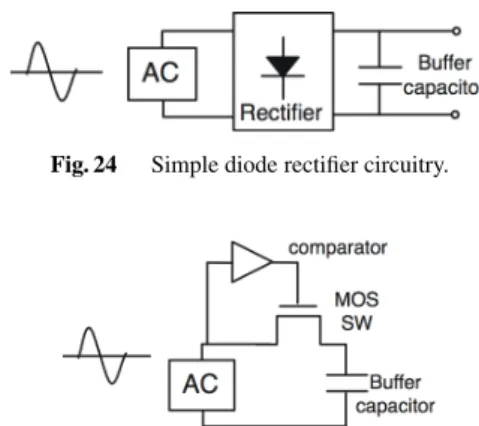
Fig. 24 Simple diode rectifier circuitry.
Fig. 25 Simplified ideal diode rectifier circuitry.
4.1 DC Output Harvesters
The output voltages from PVCs and TEGs are DC but are too low to charge a power storage directory. Thus a high- performance DC-DC converter with an ultralow start-up voltage, a high input voltage, a high power supply rejec- tion ratio (PSRR) and a low standby current is required [16].
Regarding the buffer power storage, an ultralow leakage cur- rent and low output impedance drive the RF transceiver of WSN nodes [17].
4.2 AC Output Harvesters
On the other hand, RF harvesters and VEHs generate an AC voltage. These harvesters require an additional rectifier that acts as an AC-DC converter. For the case of a large har- vested output and a cyclic voltage, simple full bridge diode circuitry can be used as the AC-DC converter (Fig. 24).
However, for a very low or unstable output voltage from a harvester, the losses due to the drop in the forward voltage of the diode are significant. A low-power MOS switch and a low-power comparator are typically used in ideal diode circuitry (Fig. 25). The circuitry consumes little energy but can reduce the diode losses [18].
The output waveforms from some VEHs do not have a purely sinusoidal shape and the output frequency is random.
To improve the harvesting power efficiency of VEHs, a step- up and step-down converter with a low DC resistance (DCR) choke inductor using SSHI (synchronized switch harvest- ing on induction) peak detection and control circuitry [19]
is widely used in energy harvesting. As shown in Fig. 26, SSHI circuitry is typically used for high-efficiency AC-DC conversion and combined with high-efficiency DC-DC con- version circuitry to charge the battery or capacitor.
Finally, the output voltage, impedance, distortion and frequency vary considerably among harvesters. For exam- ple, electrostatic VEHs have very high output impedance and voltage but are strongly affected by the parasitic capaci- tance. Thus, the success of energy harvesters hinges on fur- ther improving the circuit technology to realize low power and high capability regardless of the characteristics of the
Fig. 26 Example of SSHI circuitry for VEH.
harvester.
5. Conclusion
This paper gives an overview of energy harvesters and presents two types of vibratory energy harvester with electrostatic and electromagnetic mechanisms for human- monitoring applications that have been developed in our project. These energy harvesters require further improve- ment, but are expected to be suitable power sources for fully autonomous systems with the support of high-performance analog and digital integrated circuitry.
Acknowledgments
This research was supported by the Exploratory Research for Advanced Technology (ERATO) scheme of Japan Sci- ence and Technology Agency (JST). The author would like to thank all members of the MEMS and Circuits Lab. of the University of Hyogo.
References
[1] J.G. Ko, C. Lu, M.B. Srivastava, and J.A. Stankovic, “Wireless sen- sor networks for healthcare,” Proc. IEEE, vol.98, no.11, pp.1947–
1960, Nov. 2010.
[2] B. Cook, S. Lanzisera, and K. Pister, “SoC issues for RF smart dust,”
Proc. IEEE, vol.94, no.6, pp.1177–1196, June 2006.
[3] P. Mitcheson, E. Yeatman, G. Rao, S. Holmes, and T. Green, “En- ergy harvesting from human and machine motion for wireless elec- tronic devices,” Proc. IEEE, vol.96, no.9, pp.1457–1486, Sept. 2008.
[4] K. Maenaka, “Human activity monitoring by MEMS sensing fu- sion,” Proc. 23rd Int. Microprocesses and Nanotechnology Conf., Kokura, Japan, 10C-2-1, Nov. 2010.
[5] K. Maenaka, K. Masaki, and T. Fujita, “Application of multi en- vironmental sensing system in MEMS technology — Monitoring of human activity,” Proc. 4th Int. Conf. Networked Sensing Systems, Braunschweig, Germany, pp.47–52, June 2007.
[6] R. Vullers, R. Schaijk, I. Doms, C. Hoof, and R. Mertens, “Mi- cropower energy harvesting,” Solid-State Electron., vol.53, no.7, pp.684–693, July 2009.
[7] T. Torfs, V. Leonov, C. Hoof, and B. Gyselinckx, “Body-heat pow- ered autonomous pulse oximeter,” Proc. 5th IEEE Conf. Sensors, pp.427–430, Daegu, Korea, Oct. 2006.
[8] K. Matsumoto, K. Saruwatari, and Y. Suzuki, “Vibration-power battery-less sensor node using MEMS electret generator,” Proc.
Power MEMS 2011, pp.134–137, Seoul, Korea, Nov. 2011.
[9] MPG-D651 MPG-D751, Thin Film Thermogenerators and Sensing Devices, datasheet, http://www.micropelt.com/down/datasheet mpg
d651 d751.pdf, accessed March 27. 2013.
[10] P. Mitcheson, Analysis and optimization of energy-harvesting micro-generator systems, Ph. D Thesis, University of London, 2005.
[11] K. Fujii, T. Toyonaga, T. Fujita, Y. Jiang, K. Higuchi, and K.
Austria, Sept. 2010.
[13] T. Fujita, K. Fujii, T. Onishi, K. Kanda, K. Higuchi, and K.
Maenaka, “Electret energy harvester vibrated at collision induced natural frequency,” Proc. Eurosensors XXV, pp.733–736, Athens, Greece, Sept. 2011.
[14] S. Miki, T. Fujita, T. Kotoge, Y. Jiang, M. Uehara, K. Kanda, K.
Higuchi, and K. Maenaka, “Electromagnetic energy harvester by us- ing buried NdFeB,” Proc. IEEE MEMS2012, pp.1221–1224, Paris, France, Jan. 2012.
[15] T. Fujita, T. Onishi, K. Fujii, K. Kanda, K. Higuchi, and K.
Maenaka, “Evaluation of the human vibration for autonomous power source,” Proc. World Automation Congress (WAC2012), pp.1–4, Puerto Vallarta, Mexico, June 2102.
[16] LTC3108, Ultralow Voltage Step-Up Converter and Power Man- ager, datasheet, http://cds.linear.com/docs/en/datasheet/3108fb.pdf, accessed March 27. 2013.
[17] Chip-type Electric Double Layer Capacitor, “CPX” series come to the market It is ideal for Energy-Harvesting and Wireless Sensor Network, press releases, http://www.sii.co.jp/corp/pr/newsDetail en.
jsp?news=50987, accessed March 27. 2013.
[18] M. Wischke, G. Biancuzzi, G. Fehrenbach, Y. Abbas, and P. Woias,
“Vibration harvesting in railway tunnels,” Proc. Power MEMS2010, pp.123–126, Leuven, Belgium, Nov. 2010.
[19] J. Dicken, P. Mitcheson, I. Stoianov, and E. Yeatman, “Power- extraction circuits for piezoelectric energy harvesters in miniature and low-power applications,” IEEE Trans. Power Electron., vol.27, no.11, pp.1–16, 2012.
Takayuki Fujita received his B.E., M.E., and Ph.D. degrees from Himeji Institute of Technology, Japan, in 1995, 1997, and 2000, respectively. From 2001 to 2004 he was a Re- search Associate at Himeji Institute of Technol- ogy. Since 2007 he is an Associate Professor in the Department of Electrical Engineering and Computer Sciences, University of Hyogo. His research topics are MEMS sensor systems and energy-harvesting devices.

![Fig. 13 Harvested power vs applied acceleration at optimum load resistance ( c 2010, Elsevier [13]).](https://thumb-ap.123doks.com/thumbv2/123deta/5626294.1500270/4.892.145.355.425.596/fig-harvested-power-applied-acceleration-optimum-resistance-elsevier.webp)
![Fig. 23 Harvesting results for a short walk in the test field ( c 2011, IEEE [15]).](https://thumb-ap.123doks.com/thumbv2/123deta/5626294.1500270/6.892.226.669.802.1091/fig-harvesting-results-short-walk-test-field-ieee.webp)