Demonstration of n-Type SnS in
Bulk Ceramics and Single Crystal by
Anion Substitution
2020 年 3 月
井口 雄喜
2
Demonstration of n-Type SnS in
Bulk Ceramics and Single Crystal by
Anion Substitution
山梨大学大学院
医工農学総合教育部
論文博士学位論文
2020 年 3 月
井口 雄喜
Table of contents
1. General Introduction ... 1
1-1. Usage transition of solar energy ... 1
1-2. SnS, as a next generation solar cell material ... 3
2. n-Type conduction in SnS by anion substitution with Cl ... 12
2-1. Introduction ... 12
2-2. Experimental ... 13
2-3. Results and discussion ... 13
2-4. Summary... 17
3. Segregation of chlorine in n-type tin monosulfide ceramics: Actual chlorine concentration for carrier-type conversion ... 26
3-1. Introduction ... 26
3-2. Experimental ... 28
3-3. Results and Discusion ... 29
3-4. Summary... 33
4. Single-crystal growth of Cl-doped n-type SnS using SnCl2 self-flux ... 43
4-1. Introduction ... 43
4-2. Experimental ... 44
4-3. Results and Discussion ... 45
4-4. Summary... 48
5. General Conclusion ... 57
Publication lists ... 60
1
1. General Introduction
1-1. Usage transition of solar energy
Humankind has used the benefits of the sun in various ways until now. For example, plant-based foods such as vegetables and fruits accumulate chemical energy converted from sun light energy through photosynthesis. The time humans relied on food collection from nature to the beginning of agriculture and the following the modern agriculture, humankind utilizes solar energy whether intended or not. With the progress of the times, natural engines such as windmills and water turbines have been used in agriculture. At that time, they were affected by atmospheric circulation due to solar energy. It can be said that part of the solar energy is converted to kinetic energy. Burning wood, in which chemical energy converted from solar energy is concentrated, were converted into heat energy for a long time until now.
After the industrial revolution, technologies have been dramatically developed and the energy sources becoming mainstream instead of heating wood or other renewable natural energy were fossil fuels such as coal and oil; however these energy sources are concentrated chemical energy converted from solar energy, a long, long time ago. All of these are benefit of solar energy. The main form of energy which we are using now is electrical energy, and then we naturally think how we convert solar energy directly to electrical energy without intercalary chemical energy.
Solar cells are devices that convert sunlight directly into electrical energy, and are demonstrated with advances in semiconductor technology. The first
2
solar cell based on pn homo-junction using single crystal Si was demonstrate in 1954 by Chapin et al. [1] Solar cells are considered from the start as semiconductor applications; only 5-year later from the Shockley publication that the concept of pn junctions in 1949. [2]
Since then, for over half a century, Si-based solar cells have been extensively studied not only in single crystals but also in various forms such as polycrystalline Si and amorphous Si, resulting that the cost and physical properties have been improved. [3-7] We can produce not only intrinsic Si but also intentionally hole and electron doped Si, i.e. p- and n-type Si. Carrier type tunable Si is suitable demonstration of pn homo-junction solar cell: homo-junction avoids formation of defects at the p-n junction interface if different p- and n-type materials were employed. The defects at the interface drastically decreased solar cell efficiency so we have to develop additional techniques to avoid them.
On the other hand, in order to improve the performance of solar cells which cannot overcome by Si solar cells, compound semiconductors based solar cells were energetically studied. A specific example of a physical problem of Si is the low absorption coefficient just above band gap energy. Since Si is an indirect-transition semiconductor, the light absorption coefficient close to the band gap is small, and thick layers are required to absorb light sufficiently, and the amount of Si used will inevitably increase. [8-10]
In contrast, there are a lot of compound semiconductors which have direct- type transition: GaAs, Cu(InGa)Se2 (CIGS), which is a mixed crystal of CuInSe2 and CuGaSe2, and CdTe. [11-15] Direct-transition semiconductors have
3
high absorption coefficient, so they can be made thinner films compare with Si based solar cells. However, they still have problems: GaAs is too expensive to use home and industrial on the earth so it was used in satellites. CIGS are multiple elements compounds, meaning that unique technology development for composition control with high accuracy. CIGS and CdTe are used as p-type layers so hetero-junction and multi-layered structure. As a result, highly refining techniques are required. In addition, these compounds semiconductor use toxic elements: As, Se, Cd, and Te.
In recent years, not only cost and performance, but also environmental compatibility has been regarded as important: inexpensive, non-toxic elements and so on. From this point of view, GaAs, CIGS, and CdTe are not suitable for the next generation solar cell materials, and new non-toxic, safe and earth abundant materials are desired. Discovery of new materials possibly solve the problems.
1-2. SnS, as a next generation solar cell material
As next generation compound solar cell materials with toxic elements that are harmful to the human should avoided as much as possible from the viewpoint of environmental compatibility. In other words, they must be composed of elements commonly found in our living environment as no-toxic materials. Further, in terms of physical properties, it is necessary to have a high mobility and high absorption coefficient compere to those of existing materials such as Si and CIGS. Cu2(Zn,Sn)(S,Se)4 (CZTS) is an attracting semiconductor
4
as a next-generation compound solar cell material that can be used as an alternative material of CIGS, and is actively researched and developed. [16-18]
The compound semiconductor solar cell materials used today have a high absorption coefficient, which is partly due to having an electronic structure of d10 closed shell orbitals, for examples, Cu+ in CIGS and Cd2+ in CdTe. d-d transition could be origin of weak absorption coefficient because of they are forbidden transition. i.e. closed shell electronic configuration such as d0, d10, and d10s2 orbitals are one of the key feature for requirements to demonstrate high absorption coefficient from just above band gap energy.
Based on these ideas, I focused on tin-monosulfide, SnS, in which Sn2+ ions and S2– ions has closed shells of 4d105s2 and 4p6, respectively if it is an ionic compound, as a potential candidate for the next generation solar cell material. Sn is an element that is environmentally friendly material as can be used as canned foods, and S is a common element contained in the human body so that it is contained in a large amount in hair. In this material, Sn2+ ions have a 4d105s2 electronic configuration, and spherical 5s orbitals possibly lead high hole mobility. In fact, SnS naturally show p-type conduction. [19-22] In addition, other physical properties such as absorption efficiency, calculated electron and hole effective masses, band gap energy, and etc. are suitable for high efficient solar cell and the estimated ideal conversion efficiency is ~25%, which is comparable to those of Si and other compound semiconductors. [23-32]
SnS naturally shows p-type conduction without intentional doping because tiny discrepancy of composition ratio of 1 easily creates shallow acceptor level; both of Sn rich and poor conditions make shallow acceptor levels.[25,33] To
5
provide high efficient solar cell, especially to get high open circuit voltage (Voc), pn homo-junction is ideal; because full width of band gap energy possibly contribute to the high Voc, there is no band-offset at the interface so minority carriers flow to the other side without over any energy barrier, and any counterplan of lattice mismatch at the interface was not required: Defects at the interface are well known as very effective carrier recombination centers. [34,35]
There had been no n-type SnS and so reported SnS based solar cells were composed of heterojunction structure in which CdS and Zn(O,S) were used as n-type layer. However, as mentioned above, heterojunction reduce the conversion efficiency because of lattice and band mismatches at the interfaces and the reported highest conversion efficiency is limited to less than 5%.[36-42] In other words, I believe that if n-type SnS can be realized, it will be a foothold for raising the conversion efficiency to a practical level.
Actually, there are some reports related to n-type SnS; however they do not show solid evidence of mobile electron was doped into SnS because one of the reports required annealing in the air atmosphere, which is the conditions to produce SnO2, which is a typical n-type conductor. [43-47] other reports exhibit the existence of SnS2 and/or Sn2S3, which are also n-type conductors. [48-53] Only reliable report on the n-type SnS is that the substitutional Pb doping for Sn is effective for demonstrating n-type conduction; however the Pb concentration for conduction type conversion is more than 20%, reducing advantage of SnS that is the component elements are non-toxic. [54-55] Therefore, to say the least, there is still no n-type SnS that retains the benefits of SnS, such as environmentally friendly (non-toxic).
6
That is to say, there are two routes were reported for carrier-type conversion from p- to n-type so far; one has been attempted has attempted to replace trivalent cations with Sn sites, and the other is utilizing its layered structure and replacing Sn with divalent Pb to open up the inter-layer distances, facilitating the incorporation of Sn ions in there. [56-60] As a result, the incorporated Sn supplies carrier electrons. A new approach is necessary to realize n-type SnS with high environmental compatibility. In this thesis, I will demonstrate of environmental friendly n-type SnS, which has never been realized before, and reveal its physical properties.
7
References
[1] D. M. Chapin, C. S. Fuller and G. L. Pearson, J. Appl. phys., 25, 676 (1954). [2] W. Shockley, Bell Sys. Tech., 435 (1949)
[3] T. Matsui, A. Bidiville, K. Maejima, H. Sai, T. Koida, T. Suzuki, M. Matsumoto, K. Saito, I. Yoshida and M. Kondo, Appl. Phys. Lett., 106, 053901 (2015)
[4] F. Haase, C. Hollemann, S. Schafer, A. Merkle, M. Rienacker, J. Krugener, R. Brendel, and R. Reibst, Sol. Energy Mater. sol. cells, 186, 184 (2018)
[5] J. Zhao, A. Wang and M. A. Green, Prog. Photovolt: Res. Appl., 7, 471 (1999) [6] T. Saga, NPG Asia Mater., 2, 96 (2010)
[7] M. Green, Y. Hishikawa, E. Dunlop, D. H. Levi, J. Hohl-Ebinger, and A. W. Y. Ho-Baillie, Prog. Photovolt: Res. Appl., 26, 3 (2018)
[8] D. E. Carlson and C. R. Wronski, Appl. Phys. Lett., 28, 671 (1976) [9] M. Green and M. J. Keevers, Prog. Photovolt: Res. Appl., 3, 189 (1995)
[10] T. Tiedje, E. Yablonovitch, G. D. Cody, and B. G. Brooks, IEEE Trans. Electron
Devices, 31, 711 (1984)
[11] S. Richard, F. Aniel and G. Fishman, Phys. Rev. B, 70, 235204 (2004) [12] J. E. Jaffe and A. Zunger, Phys. Rev. B, 29, 1882 (1984)
[13] L. Liborio, S. C. Chew and N. Harrison, Surf. Sci., 606, 496 (2012)
[14] A. Soni, A. Dashora, V. Gupta, C. M. Arora, M. Rerat, B. L. Ahuja and R. Pandey,
Journal of Elec. Materi., 40, No.11 (2011)
[15] E. Deligoz, K. Colakoglu and Y. Ciftei, Physica B, 373, 124 (2006)
[16] T. P. Dhakal, C. Y. Peng, R. R. Tobias, R. Dasharathy and C. R. Westgate, Sol.
Energy, 100, 23 (2014)
8
Takeuchi, Thin solid films, 517, 2455 (2009)
[18] H. Katagiri, K. Jimbo, M. Tahara, H. Araki and K. Oishi, Mater. Res. Soc. Symp.
Proc. 1165, 1165-M04-01 (2009)
[19] W. Albers, C. Haas, H. J. Vink and J. D. Wasscher, J. Appl. phys., 32, 2220 (1961) [20] Y. F. Guastavino and C. Llinares, J. Mater. Sci. Lett., 19, 2135 (2000)
[21] S. S. Hegde, A. G. Kunjomana, K. A. Chandrasekharan, K. Ramesh nad M. Prashantha, Phys. Rev. B, 406, 1143 (2011)
[22] F. Y. Ran, Z. Xiao, H. Hiramatsu, K. Ide, H. Hosono and T. kamiya, AIP Advances,
6, 015112 (2016)
[23] M. Parenteau and C. Carlone, Phys. Rev. B, 41, 5227 (1990)
[24] R. E. Banai, H. Lee, M. A. Motyka, R. Chandrasekharan, N. J. Podraza, J. R. S. Brownson and M. W. Horn, Journal of Photovoltaic, 3, 1084 (2013)
[25] J. Vidal, S. Lany, M. d'Avezac, A. Zunger, A. Zakutayev, J Francls and J. Tate,
Appl. Phys. Lett., 100, 032104 (2012)
[26] J. Park, M. Song, W. M. Jung, W. Y. Lee, J. Lee, H. Kim and II-Wun Shim, Bull
Korean Chem. Soc., 33, 3383 (2012)
[27] J. J. Lofeski, J. Appl. phys., 27, 777 (1956)
[28] S. Lin, X. Li, H. Pan, H. Chen, X. Li, Y. Li and J. Zhou, Superlattices and
Microstructure, 91, 375 (2016)
[29] W. C. Dash and R. Newman, Phys. Rev., 99, 1151 (1955) [30] A. E. Rakhshani, J. Appl. phys., 81, 7988 (1997)
[31] H. C. Casey Jr., D. D. Shell and K. W. Wecht, J. Appl. phys., 46, 250 (1975) [32] J. Tuttle, D. Albin, J. Goral, C. Kennedy and R. Noufi, Sol. Cells, 24, 67 (1988) [33] B. D. Malone, A. Gali and E. Kaxiras, Phys. Chem. Chem. Phys., 16, 26176
9
(2014)
[34] A. Kanevce, I. Repins and S. H. Wei, Sol. Energy Mater. Sol. cells, 133, 119 (2015)
[35] R. H. Blue, Sol. cells, 23, 1 (1988)
[36] K. T. R. reddy, N. K. Reddy and R. W. Miles, Sol. Energy Mater. Sol. cells, 90, 3041 (2006)
[37] L. Sun, R. Haight, P. Sinermsuksakui, S. B. Kim, H. H. Park and R. G. Gordon, J.
Appl. phys. lett., 103, 181904 (2013)
[38] J. Jhon, M. Vequizo and M. Ichimura, Jpn. J. Appl Phys, 51, 10NC38 (2012) [39] S. Gedi, V. R. M. Reddy, B. Pejjai, C. W. Jeon, C. Park and K. T. R. Reddy, Appl.
Surf. Sci. 372, 116 (2016)
[40] H. H. Park, R. Heasley, L, Sun, V. Steinmann, R. Jaramillo, K. Hartman, R. Chakraborty, P. Sinsermsuksakul D. Chua, T. Buonassisi and R. G. Gordon,
Progress in Photovoltaics, 23, 901 (2015)
[41] V. Steinmann, R. Jaramillo, K. Hartman, R. Chakraborty, R. E. Brandt, J. R. Poindexter, Y. S. Lee, L, Sun, A. Polizzotti, H. H. Park, R. G. Gordon and T. Buonassisi, Adv. Mater., 26, 7488 (2014)
[42] P. Sinsermsuksakul, L. Sun, S. W. Lee, H. H. Park, S. B. Kim, C. Yang and R. G. Gordon, Adv. Energy Mater., 1400496 (2014)
[43] T. H. Sajeesh, A. R. Warrier, C. S. Kartha, K. P. Vijayakumar, Thin Solid Films,
518, 4370 (2010)
[44] P. A. Nwofe, K. T. R. reddy and R. W. Miles, Photovoltaic Specialists IEEE Conference, 14115963 (2013)
10
[45] P. K. Nair, M. T. S. Nair, R. A. Zingaro and E. A. Meyers, Thin Solid Films, 239, 85 (1994)
[46] J. Bandara, C. M. Divarathne and S. D. Nanayakkara, Sol. Energy Mater. Sol. cells,
81, 429 (2015)
[47] S. C. Ray, M. K. Karanjai and D. D. Gupta, Thin Solid Films, 350, 72 (1999) [48] A. Dussan, F. Mesa and G. Gordillo, J. Mater. Sci., 45, 2403 (2010)
[49] T. J. Whittles, L. A. Burton, J. M. Skelton, A. Walsh, T. D. Veal and V. R. Dhanak,
Chem. Mater., 28, 3728 (2016)
[50] D. J. Singh, Appl. Phys. Lett., 109, 032102 (2016)
[51] T. S. Reddy and M. C. S. Kumar, Ceramics International, 42, 12262 (2016) [52] C. Julien, M. Eddrief, I. samaras and M. Balkanski, Mat. Sci. Eng. B, 15, 70
(1992)
[53] A. Sanchez-Juarez, A. Tiburcio-Silver and A. Ortiz, Thin Solid Films 480, 452 (2005)
[54] Z. Xiao, F. Y. Ran, H. Hosono and T. Kamiya, Appl. Phys. Lett., 106, 152103 (2015)
[55] F. Y. Ran, Z. Xiao, Y. Toda, H. Hiramatsu, H. Hosono and T. Kamiya, Sci. Rep., 5:10428 (2015)
[56] S. H. Chaki, M. D. Chaudhary and M. P. Deshpande, Mater. Res. Bull., 63, 173 (2015)
[57] P. Sinsermsuksakul, R. Chakraborty, S. B. Kim, S. M. Heald, T. Buonassisi and R. G. Gordon, Chem. Mater., 24, 4556 (2012)
[58] K. S. Kumar, C. Manoharan, S. Dhanapandian, A. G. Manohari and T. Mahalingam, Optik, 125, 3996 (2014)
11
[59] H. T. Hsu, M. H. Chiang, C. H. Huang, W. T. Lin, Y. S. Fu and T. F. Guo, Thin
Solid Films, 584, 37 (2015)
[60] M. Seal, N. Singh, E. W. Mcfarland and J. Baltrusaitis, J. Phys. Chem. C, 119, 6471 (2015)
12
2. n-Type conduction in SnS by anion substitution with Cl
2-1. Introduction
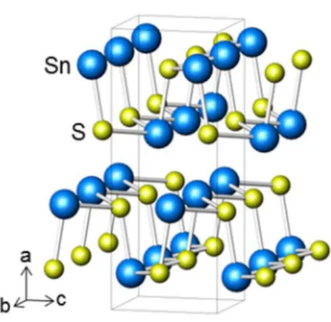
SnS is a promising photovoltaic semiconductor because its band gap energy (~1.07 eV)[1-3] and high optical absorption coefficient (~104–105 cm–1)[1,4-6] are suitable for high efficiency solar cells,[7,8] and its chemical composition consists only of nontoxic and earth abundant elements. As shown in Fig. 1, SnS has a layered crystal structure in which each (SnS)2 layer is stacked along the
a-axis. SnS naturally shows p-type conduction because of the low formation
enthalpy of Sn vacancies.[3,6,9] Although the formation of n-type SnS by substitutional aliovalent cation doping at Sn sites has been investigated, no reliable successful result has been reported.[1,2,6,10,11] Thus, heterojunctions with n-type CdS or n-type wide gap oxides such as ZnO and SnO2 have been employed in solar cells. However, unfavorable band alignments at the heterojunction interfaces of SnS-based solar cells reduce their energy conversion efficiencies to 1%–4.36%, relative to their theoretical efficiency computed from the SnS bandgap (~24%)[4,12-14] and the calculated efficiencies of heterojunction solar cells fabricated from n-type semiconductors such as CdS and ZnS (6.03%–16.26%).[15] Recently, reliable n-type SnS has been achieved by isovalent cation doping; for example, Sn(II)1–zPb(II)zS exhibits
n-type conduction at z ≥ 0.2, with a maximum electron Hall mobility of 7.0 cm2/Vs and an estimated extended mobility of 160 cm2/Vs in highly oriented polycrystalline film.[3] However, the use of Pb, which is a toxic element, offsets the advantages of the use of SnS. On the other hand, anion substitution in SnS
13
has yet to be examined. In this study, I achieved n-type bulk SnS ceramics by substitution with the aliovalent anion Cl−, which is less toxic than Pb, and clarified that Cl doping generates the n-type conversion, while S site deficiency determines the free electron density.
2-2. Experimental
Undoped and Cl-doped SnS powders were synthesized by solid-state reaction with ground Sn metal (Sigma Aldrich Co., 99.999%), sulfur powder (Kojundo Chem. Lab. Co., Ltd. 99.999%), and SnCl2 (Kojundo Chem. Lab. Co., Ltd. 99.9%). To prevent oxidation of the starting materials, the Sn metal was ground and then mixed with the sulfur and SnCl2 powders in a glovebox filled with dry nitrogen. The mixed powders were heated at 520 °C for 12 h in silica tubes evacuated to ~4 Pa. The obtained powders were sintered by the spark plasma sintering (SPS) method at 580 °C for 6 min in a vacuum (~10 Pa). These synthesis processes caused unintentional sulfur deficiency, as confirmed by wavelength-dispersive X-ray fluorescence spectroscopy (WD–XRF) and inductively-coupled plasma atomic emission spectroscopy (ICP–AES). Therefore, the samples are described as Sn(S1–x–yClx). The obtained samples
had a high relative density (~90%).
2-3. Results and discussion
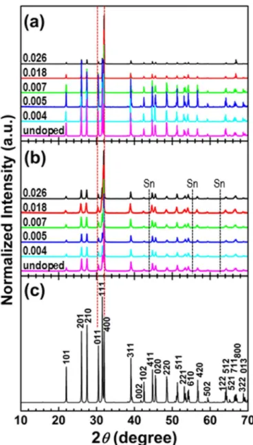
Figure 2 compares the powder X-ray diffraction (XRD) patterns of the undoped Cl-doped powders (a) and the high density disks (b) with the simulated pattern (ICDD-PDF no. 01-073-1859) (c). Panels (a) and (b) also
14
indicate the Cl compositions x in Sn(S1–x–yClx), measured by WD–XRF using
the calibration curve method. As the obtained crystal grains were plate-like in shape, (h00) was the preferential orientation in the XRD patterns of both powders and disks. The XRD measurements revealed single-phase powders with no impurity phases such as Sn2S3 and SnO2. However, the sintered disks contained small quantities of Sn metal impurities, which were uniformly distributed throughout the bulk ceramics. The Sn metal content was estimated as less than 0.8 at.% by Rietveld analysis. Thus, I considered that the Sn impurity did not affect the electrical properties of the obtained samples, especially their conduction types and carrier mobilities.
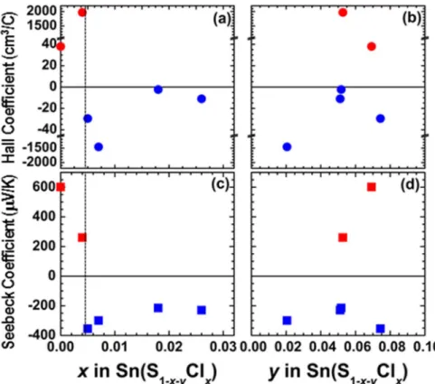
The conduction types of the undoped and Cl-doped ceramic samples were confirmed by measuring the Seebeck and Hall coefficients at room temperature (RT). The Hall measurements were performed in the van der Pauw configuration with planar samples of thickness 1.60–0.17 mm. The obtained results are summarized in Fig. 3. Both the Seebeck and Hall coefficients were positive in pure SnS and slightly Cl-doped Sn(S0.096–yCl0.004) (with x = 0 and 0.004 respectively), indicating that these samples are p-type conductors. Conversely, the coefficients of more heavily doped samples (x ≥ 0.005) were negative, substantiating the n-type conduction in Cl-doped SnS. I emphasize that all samples contained S site deficiencies (y = 0.021–0.074, estimated by ICP–AES). As seen in panels (b) and (d) of Fig. 3, y did not control the conduction type conversion.
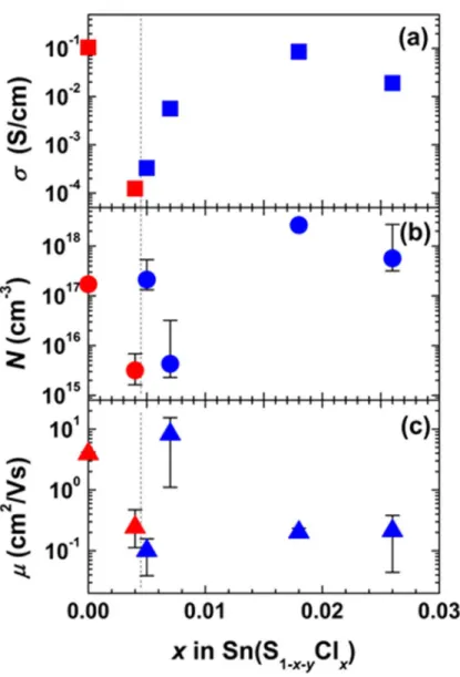
Figure 4 shows the electrical conductivity (σ), carrier density (N), and mobility (μ) at RT obtained in the Hall effect measurements. First, doping with
15
0.4 at.% Cl (x = 0.004) reduced the σ of SnS by three orders of magnitude. This result is attributed to the reduction of both N and μ. The σ of the x = 0.005 sample was similar to that at x = 0.004, but its conduction type was reversed as discussed for Fig. 3. Further Cl doping from x = 0.005 to 0.018 increased the σ, but did not systematically alter the N and μ values (Fig. 4(b) and (c)). Similarly scattered data were reported at small Pb concentrations in n-type Sn1–zPbzS.[3]
However, although N and μ are uncorrelated with x, both factors are relatively well-correlated with respect to the S site deficiency y, as shown in Fig. 5(a) and (b). Here I should recall that the S site deficiencies (y = 0.021–0.074) are larger than the Cl doping concentration (x ≤ 0.026). Accordingly, I conclude that the Cl doping induces n-type conduction, while the S site deficiency enhances the free electron carrier density in the n-type samples. Note that the reported formation enthalpy of S vacancy in pure SnS under an S-poor condition by theoretical calculations is lower than that of interstitial Sn,[3,6,9] indicating that the S vacancy in Cl-doped SnS can be the origin of an additional electron carrier. On the other hand, as shown in Fig. 5(b), increasing the S site deficiency decreased the mobilities in n-type samples. The maximum electron mobility (8.3 cm2/Vs) was achieved at the smallest S site deficiency (x = 0.007; y = 0.021). This mobility exceeds that obtained in thin films of n-type Sn1–zPbzSn (with a Hall mobility of 7.0 cm2/Vs).[3]
To compare the carrier transport properties between our dense ceramic samples and previously-reported high quality films, I measured the temperature dependence of N and μ in our undoped p-type SnS0.931 sample (Fig. 6 (a)–(c)). In this sample, N exhibited a thermal activation-type behavior with an
16
activation energy of 36 meV. The Hall mobility was significantly temperature-dependent, as seen in Fig. 6(b) and (c). Many polycrystalline semiconductors follow the grain boundary potential barrier model proposed by Seto et al.[16] In this model, the temperature dependence of µ is given by
= exp (− / ) (1)
Here, µ0 = (2 ∗ ) ⁄ is the extended mobility without the grain boundary effect (where L, q, m*, and kB are the grain size, the elementary electric charge, the effective mass, and the Boltzmann constant, respectively). Theln ⁄ − plots of the undoped sample (Fig. 6(b)) were linear over the whole measured temperature range, indicating that the grain boundary potential barrier model describes the main scattering mechanism, as previously reported for high-quality film.[2] The grain boundary potential height EB and extended mobility μ0 of the undoped p-type sample were estimated as 86 meV and 140 cm2/Vs, respectively; the latter is again consistent with the previously reported mobility in high quality film (~200 cm2/Vs).[2]
To clarify the origin of the low mobility in the highly doped (N = 2.6 × 1018 cm–3) n-type sample (SnS
0.930Cl0.018), I measured the temperature dependence
of N and μ in this sample. As shown in Fig. 6(d), the N of the n-type sample was not significantly related to temperature, indicating a degenerated semiconductor. Conversely, the Hall mobility was clearly temperature-dependent, as shown in Fig. 6(e) and (f). From the slope of Fig. 6 (e) and Eq. (1), the extended mobility μ0 was calculated as 0.78 cm2/Vs, much smaller than in n-type Sn0.52Pb0.48S (160 cm2/Vs), whose N (4.3 × 1013 cm3) was three orders of magnitudes smaller than that of SnS0.930Cl0.018.3) To further
17
clarify the scattering mechanism, I examined double-logarithmic plots of the Hall mobilities in the p- and n-type samples as functions of temperature, and measured their slopes as 2.9 and 1.5, respectively [see panels (c) and (f) of Fig. 6]. The former plot is not completely linear, and the slope of 2.9 is not explained by usual scattering models.[17] This result supports the above conclusion that the grain boundary potential barriers control the hole transport in the undoped p-type SnS0.931 sample. On the other hand, the slope of 1.5 for the Cl-doped n-type sample is consistent with the ionized impurity scattering model.[17] Accordingly, I conclude that ionized impurity scattering dominates in Cl-doped n-type SnS0.930Cl0.018.
2-4. Summary
In summary, this study achieved n-type SnS by low-dose substitution of the aliovalent anion Cl– at the S2− sites. The maximum electron mobility was 8.3 cn2/Vs. Both the Cl concentration and S site deficiency appear to be important for realizing n-type SnS with high carrier density. The dispersion of carrier density and electron mobility were probably induced by the unintentional variation in S site deficiencies.
18
References
[1] W. Albers, H. J. Vink, C. Haas, and J. D. Wasscher, J. Appl. Phys. 32, 2220 (1961).
[2] F.-Y. Ran, Z. Xiao, H. Hiramatsu, H. Hosono, and T. Kamiya, Appl. Phys. Lett.
104, 072106 (2014).
[3] F.-Y. Ran, Z. Xiao, Y. Toda, H. Hiramatsu, H. Hosono, and T. Kamita, Sci. Rep. 5, 10428 (2015).
[4] H. Noguchi, A. Setiyadi, H. Tanamura, T. Nagamoto, and O. Omoto, Sol. Energy Mater. Sol. Cells 35, 325 (1994).
[5] P. Sinsermsuksakul, J. Heo, W. Noh, A. S. Hock, and R. G. Gordon, Adv. Energy Mater. 1, 1116 (2011).
[6] J. Vidal, S. Lany, M. d’Avezac, A. Zunger, A. Zakutayev J. Francis, and J. Tate, Appl. Phys. Lett. 100, 032104 (2012).
[7] J. J. Loferski, J. Appl. Phys. 27, 777 (1956).
[8] W. Schockley and H. J. Queisser, J. Appl. Phys. 32, 510 (1961).
[9] Z. Xiao, F.-Y. Ran, H. Hosono, and T. Kamiya, Appl. Phys. Lett. 106, 152103 (2015).
[10] A. Dussan, F. Mesa, and G. Gordillo, J. Mater. Sci. 45, 2403 (2010).
[11] P. Sinsermsuksakul, R. Chakraborty, S. B. Kim, S. M. Heald, T. Buonassisi, and R. G. Gordon, Chem Mater. 24, 4556 (2012).
[12] A. Schneikart, H. -J.Schimper, A. Klein, and W. Jaegermann, J. Phys. D: Appl. Phys. 46, 305109 (2013).
[13] V. Steinmann, R. Jaramillo, K. Hartman, R. Chakraborty, R. E. Brandt, J. R. Poindexter, Y. S. Lee, L. Sun, A. Polizzotti, H. H. Park, R. G. Gordon, and T.
19
Buonassisi, Adv. Mater. 26, 7488 (2014).
[14] V. R. M. Reddy, S. Gedi, C. Park, R.W. Miles, and K. T. Ramakrishna Reddy,. Curr Appl. Phys. 15, 588 (2015).
[15] J. Xu and Y. Yang, Energy Conv. Manage. 78, 260 (2014). [16] J. Y. W. Seto, J. Appl. Phys. 46, 5247 (1975).
[17] P. Y. Yu and M. Cardona, Fundamentals of Semiconductors (Springer, New York, 2003) 3rd ed., p. 220.
20
Figure 1. Crystal structure of SnS. The structure consists of (SnS)2 layers stacked along the a-axis.
21
Figure 2. XRD patterns of the synthesized powders (a) and dense ceramic disks (b).
Panel (c) shows a simulated pattern (ICDD-PDF no. 01-073-1859). The numbers in (a) and (b) indicate the Cl composition (x) in Sn(S1–x–yClx). Red vertical lines show the peak
positions of the 011 and 400 diffractions. In (b), the black vertical lines show the peak positions of the Sn metal impurity. The Sn metal phase (estimated by Rietveld analysis) constitutes less than 0.8 at.% of the sample.
22
Figure 3. Hall (a) (b) and Seebeck (c) (d) coefficients at RT as functions of the Cl
composition (x) and S site deficiency (y) in Sn(S1–x–yClx). The sign conversion is
controlled by the Cl composition (x); no correlation is found for the S site deficiency (y).
23
Figure 4. Cl composition (x) dependences of electrical conductivity (a), carrier density
(b), and Hall mobility (c). The colors of the symbols indicate the conduction types (red: p-type, blue: n-type).
24
Figure 5 S site deficiency (y) dependences of carrier density (a) and Hall mobility (b) of
25
Figigure 6. Temperature dependent carrier densities and Hall mobilities of undoped p-type SnS0.931
(a) (b) (c) and Cl-doped n-type SnS0.930Cl0.018 (d) (e) (f). The red solid lines in (b) and (e) are the
linear fittings for estimating the grain boundary potential barrier height. The slopes in (c) and (f) provide the indices of the carrier scattering models.
26
3. Segregation of chlorine in n-type tin monosulfide ceramics:
Actual chlorine concentration for carrier-type conversion
3-1. Introduction
Tin monosulfide (SnS) is a promising candidate material for environmentally friendly photovoltaic semiconductors because it comprises abundant, low-cost, and non-toxic elements. In addition, the optical properties of SnS are appropriate for it to be used as active layers in single-junction solar cells with high conversion efficiency; the direct and indirect band-gap energies are estimated to be ~1.3 and ~1.1 eV, respectively.[1-4] The optical absorption coefficient of SnS is 104–105 cm−1 above 1.3 eV,[5] comparable to those of commercialized photovoltaic materials such as CuIn1–xGaxSe2 and CdTe.[6,7] To date, many SnS-based solar cells have been fabricated using various n-type materials[8-11] because SnS naturally exhibits p-type conduction. However, reliable n-type SnS was first realized in Sn(II)1–zPb(II)zS.[12] Thus, the highest
conversion efficiency of a heterojunction SnS-based solar cell achieved to date is 4.63% for the configuration of Mo/SnS/SnO2/Zn(O,S)/ZnO/ITO/Al-Ni.[13] The low conversion efficiencies of SnS-based solar cells are attributed to the trap states near heterojunctions, which result from the lattice mismatch and unfavorable band offset of n-type materials against p-type SnS. These problems could be solved by fabricating a solar cell with a homojunction configuration, i.e., p-SnS/n-SnS, for which the theoretical conversion efficiency is approximately 25%.[14] The homojunction configuration includes n-type SnS as a key component. In the case wherein n-type Sn(II)1–zPb(II)zS is used, z > 0.2 is
27
required for n-type conduction. Unfortunately, the large amount of Pb, a toxic element, detracts from the nontoxicity of SnS.
Recently, I demonstrated n-type conductive SnS by aliovalent doping with Cl–anion at the S sites of bulk ceramic samples.[15] The doped samples clearly showed conversion from p- to n-type with increasing Cl concentration, as confirmed by the negative Hall voltage and Seebeck coefficient. In addition, first-principles calculations indicated that the substitution of S with Cl increased the enthalpy of Sn vacancy formation; the formation enthalpy of Cl at the S site was sufficiently low to release an electron, particularly in the Sn-rich condition, even when the Fermi level was located near the conduction-band minimum.[16] However, the Cl-doped n-type SnS bulk ceramics exhibited an odd behavior: carrier-type conversion was clearly associated with Cl concentration, as determined via wavelength-dispersive X-ray fluorescence spectroscopy (WD–XRF), whereas electron carrier concentration (Ne) was not related to Cl concentration. In this study, I provide a reasonable explanation for this strange behavior: the segregation of Cl in bulk ceramics confused us. The carrier-type conversion and carrier concentration were clearly linked to Cl concentration in the regions of homogeneous Cl distribution.
Undoped and Cl-doped SnS (SnS1–x-δClx) were synthesized via the
conventional solid-state reaction of SnCl2 (Kojundo Chemical Laboratory Co., Ltd., 99.9%), Sn (Sigma Aldrich Co., 99.999%), and S (Kojundo Chemical Laboratory Co., Ltd., 99.9999%). The total amount of the measured reagents was ~1 g. To prevent segregation of an S-rich phase such as SnS2, which
28
exhibits n-type conduction, the Sn/S and Sn/(S + Cl) ratio was set to ~1.007. These materials were mixed in a glovebox filled with dry nitrogen. The mixed powders were heated at 520°C for 12 h in sealed silica tubes and evacuated to ~4 Pa at room temperature. The obtained sintered bodies of undoped and Cl-doped SnS were gently ground into powders. The obtained powders were sintered in high-density ceramic pellets via spark-plasma sintering (SPS) at 3.8 × 10² MPa at 580°C for 6 min in a chamber evacuated to below 10 Pa. Surface contaminants on the obtained ceramic disks were removed with waterproof sandpaper.
3-2. Experimental
WD–XRF (RIGAKU, ZSX Primus II) and electron probe microanalysis (EPMA; JEOL Ltd. JXA-8200, acceleration voltage = 15 kV, beam current ≈ 1 × 10⁻⁷ A) were used to estimate the chemical compositions of the samples in large areas ( = 1 cm) and local areas (1 × 1 μm2), respectively. Elemental mapping in 100 × 100-μm2 regions was conducted by EPMA. To avoid atmospheric contamination, the surfaces of all sintered ceramic samples were ground just before being placed into the EPMA analysis chamber. ICP-AES was used to construct a calibration curve of WD-XRF to determine the Sn/S ratios. However, the total amount of Cl was too small for detection by ICP-AES; the calibration curve of Cl was drawn using mixed powders of SnS, S, and SnCl2. I did not detect any chemical composition shifts and/or other damages caused by high-energy electron-beam irradiation during EPMA measurements. Hall effect measurements (TOYO Corp., ResiTest8300) were
29
conducted at room temperature in the van der Pauw configuration with planar samples 0.17–1.60-mm-thick to reveal the conduction type, carrier concentration, and mobility. Au was used as an ohmic electrode: Four square Au electrodes with side lengths of 3 mm were deposited on four corners of a square planar sample with a side length of 7 mm, i.e., the distances between the electrodes were 1 mm.
3-3. Results and Discusion
Figure 1 shows the elemental distributions of S (a), Cl (b), and Sn (c) along with a scanning electron microscopy (SEM) image (d) corresponding to the surface of a Cl-doped n-type sample. Cl was clearly distributed inhomogeneously in the ceramic disks; Fig. 1(b) shows a continuous blue homogeneous region with low Cl concentration (~0.2 at.%) containing the islands of high Cl concentration (> 7 at.%). The compositions of each element at the positions marked with circles in Fig. 1 are summarized in Table I. I measured five randomly selected 100 × 100-μm2 areas and selected ≥24 points for each sample; I then obtained the average Cl concentration determined by EPMA (xEPMA) and standard deviations (SD) in homogeneous regions which were determined under the assumptions that (i) the blue region of Cl mapping is of the same scale as that used in Fig 1(b) and (ii) the Sn/(S + Cl) ratio is almost unity. For example, the Cl concentration seems homogeneous at points 1 and 5 in Fig. 1(b); however, the colors indicating Sn concentration at these points in Fig. 1(c) are green and dark blue, respectively, which indicates that the points are inhomogeneous compared with the surrounding area. A
30
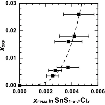
comparison of Fig. 1(c) and (d) reveals that point 1 corresponds to the slope of a mountain-range-like shape. Together with the “mountain range”, the concentration of Sn is obviously lower than the surrounding area. Similarly, point 5 corresponds to the slope of a mountain-like shape. To obtain an accurate composition, I should select a flat surface. Therefore, points 1 and 5 should be excluded from the estimation of the composition of homogeneous regions. The area shown in Fig. 1, which is one of five areas of sample No.4 in Table II, was the area in which the total area of the islands was largest. Given the total island area of sample No.4 in the five different EPMA maps, the surface ratio of the island was estimated to be ~4%. The maximum surface-area ratio of the islands was obtained for sample No.6, and the evaluated surface ratio was ~8%. I synthesized one undoped and six Cl-doped SnS samples. The Cl concentration estimated using XRF (xXRF; bulk Cl concentration; measurement area was a circle with a diameter of 1 cm) and xEPMA summarized in Table II (Cl concentration in homogenous regions) are compared in Fig. 2. The difference in the bulk and continuous Cl concentrations increased with increasing Cl concentration; at xEPMA = 0.0045, xXRF was 5.7 times larger than
xEPMA. This confirms that Cl distributed inhomogeneously in the sintered pellets, and xXRF reflected the total average Cl concentration, including the islands of high Cl concentration [Fig. 1(b)]. In addition, the number of islands increased with increasing Cl concentration. Since carriers should migrate in continuously extended homogeneous region, I conclude that considerable Cl concentration is not xXRF but xEPMA. Furthermore, the δ values in homogeneous regions of all n-type samples were almost equal (δ ≈ 0.025), meaning that
31
S-site deficiencies existed almost equally in homogeneous regions of all the n-type samples. In contrast, the Sn/S ratios of the islands with high Cl concentration are far from unity. As a result, I assume that the variations in S deficiency in bulk ceramic samples observed in our previous report[15] arise from off-stoichiometric islands and variations in their number. S-site deficiencies in homogeneous regions, which are the conduction paths of carriers, possibly generate carrier electrons equally for all n-type samples and thus, do not shift carrier concentrations and mobilities.
The segregation of Cl and off-stoichiometry in the islands in Fig. 1(a)–(c) were possibly caused by the SPS process. During SPS synthesis, current directly passes through the SnS powders, generating Joule heat. I expect that the resistance difference between the interior of the powders and the contact points between powders results in a temperature difference between them, leading to islands with a high Cl concentration and an off-stoichiometry of Sn/S.
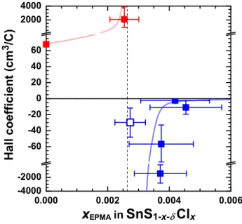
Figure 3 shows the dependence of the Hall coefficient on xEPMA. The Hall coefficients of the undoped sample and the sample with xEPMA = 0.0025 were positive, indicating that these samples showed p-type conduction. In contrast, those of the samples with xEPMA ≥ 0.0027 were negative. The dependence of the Hall coefficient on dopant concentration is usually inversely proportional because when a single carrier (hole or electron) is dominant, the Hall coefficient RH is given by
RH = 1/qN, (1)
32
(Np or Nn), where Np and Nn are hole and electron concentrations, respectively. However, for the sample with xEPMA = 0.0027, I observed a small Hall coefficient of −30 cm3/C between two inversely proportional curves, indicating that Np and Nn at xEPMA = 0.0027 were comparable; that is, both electrons and holes contributed to electric conduction, even though the Hall coefficient was negative. In such cases, the Hall coefficient is given by
RH = (Np μh2–Ne μe2)/q(Np μh + Ne μe)2, (2) where μh and μe are hole and electron mobilities, respectively. Based on these results, I can conclude that the conversion in carrier type from p- to n-type occurred at xEPMA = 0.0026. Notably, I prepared many ceramics with
xEPMA ≈ 0.0026 but reliable Hall voltages could not be obtained, suggesting that
xEPMA near 0.0026 was the boundary of the carrier-type conversion.
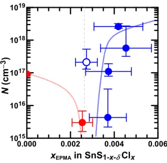
Figure 4 shows the dependence of carrier concentration on xEPMA. As mentioned earlier, indicated carrier concentration at xEPMA = 0.0027 should be neglected because it just means that both types of carriers contribute to electron conduction, and Np is slightly less than Nn; it does not mean that the actual Ne is ~1017 cm–3. By accounting for this multicarrier contribution in the conversion region, the dependence of carrier concentration on Cl concentration becomes reasonable and can be rationalized as follows. In the region of low Cl concentration, holes originate from Sn vacancies suppressed by electrons via Cl doping. In regions wherein Cl concentration was high, the number of electrons increases with increasing Cl concentration. This explains why a clear dependence of carrier concentration on Cl concentration could not be found in our previous study: the bulk Cl and S concentrations estimated by XRF did not
33
represent the local Cl and S concentrations in SnS.
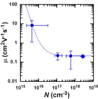
Figure 5 shows the Hall mobility as a function of carrier concentration. Hall mobility decreased with increasing carrier concentration until N ≈ 1017 cm−3, after which Hall mobility remained nearly constant at 0.2 cm2V−1s−1. This behavior can be explained via ionized impurity scattering and is consistent with our previously reported temperature dependence of Hall mobility.[15] As mentioned above, the maximum surface-area ratio of the islands was ~8%, indicating that the influence of the islands on the Hall coefficients and carrier concentrations was negligible: thus, the experimental errors would be larger than the uncertainty arising from the presence of the islands, i.e., the Cl concentration at the carrier-type conversion was reliable because it was determined from the sign of the Hall coefficient. However, if the islands were charged, then they would affect Hall mobility because ionized impurity scattering was dominant in these n-type samples.[15]
3-4. Summary
In summary, the EPMA elemental mapping of Cl-doped SnS revealed continuous homogeneous regions with relatively low Cl concentration containing the islands of high Cl concentration in which Sn/S deviated strongly from unity. The Hall coefficient and carrier concentration exhibited clear dependences on the Cl concentration in the homogeneous region. Carrier-type conversion was observed at xEPMA = 0.0026.
34
References
[1] M. Parenteau and C. Carlone, Physical Review B, 41, 5227 (1990).
[2] S. S. Hegde, A. G. Kunjomana, K. A. Chandrasekharan, K. Ramesh, and M. Prashantha, Physica B, 406, 1143 (2011).
[3] S. Cheng, Y. Chen, Y. He, and G. Chen, Materials letters, 61, 1408 (2007).
[4] J. Park, M. Song, W. M. Jung, W. Y. Lee, J. Lee, H. Kim, and II-wun Shim, Bulletin of Korean Chemical Society, 33, 3383 (2012).
[5] C. Cifuentes, M. Botero, E. Romero, C. Calderón, and G. Gordillo, Brazilian Journal of Physics, 36, 1046 (2006).
[6] J. Tuttle, D. Albin, J. Goral, C. Kenney, and R. Noufi, Solar cells, 24, 67 (1988). [7] E. Rakhshani, Journal of Applied Physics, 81, 7988 (1977).
[8] F. Jiang, H. Shen, W. Wang, and L. Zhang, Journal of the Electrochemical Society,
159, 235 (2012).
[9] K. T. R. Reddy, N. K. Reddy, and R. W. Miles, Solar energy materials and solar cells, 90, 3041 (2006).
[10] J. J. M. Vequizo and M. Ichimura, Japanese Journal of Applied Physics, 51, 10NC38 (2012).
[11] V. Steinmann, R. Jaramillo, K. Hartman, R. Chakraborty, R. E. Brandt, J. R. Poindexter, Y. S. Lee, L, Sun, A. Polizzotti, H. H. Park, R. G. Gordon, and T. Buonassisi, Advanced Materials, 26, 7488 (2014).
[12] F. -Y. Ran, Z. Xiao, Y. Toda, H. Hiramatsu, H. Hosono, and T. Kamiya, Scientific Reports, 5, 10428 (2015).
[13] P. Sinsermsuksakul, L. Sun, S. W. Lee, H. H. Park, S. B. Kim, C. Yang, and R. G. Gordon, Advanced Energy Materials, 4, 1400496 (2014).
35
[14] S. Lin, S. Li, H. Pan, H. Chen, X. Li, Y. Li, and J. Zhou, Superlattices and Microstructures, 91, 375 (2016).
[15] H. Yanagi, Y. Iguchi, and T. Sugiyama, Applied Physics Express, 9, 051201 (2016).
36
Figure 1. Elemental maps of S (a), Cl (b), and Sn (c) for the surface of a
sintered SnS1–x-δClx ceramic surface (Sample No. 4 in Table II) and the
corresponding SEM image (d). The chemical compositions of each element in the regions indicated by circles are summarized in Table I.
37
Figure 2. Bulk Cl concentration (xXRF) vs. the Cl concentration in the homogeneous regions (xEPMA) of SnS1–x-δClx samples. The dashed line is a visual guide.
0.000 0.002 0.004 0.006 0.00 0.01 0.02 0.03
x
XR Fx
EPMAinSnS
1-x-C
lx38
Figure 3. Hall coefficients of SnS1–x-δClx samples as a function of xEPMA. The solid and
open squares show data for a single carrier (holes or electrons) and multiple carriers (holes and electrons), respectively. The curved lines are visual guides.
0 20 40 60 2000 4000 H al l c o ef fi ci en t (c m 3 /C ) 0.000 0.002 0.004 0.006 -4000 -2000 -60 -40 -20 xEPMAinSnS1-x- Clx
39
Figure 4. Carrier concentration as a function of xEPMA for SnS1–x-δClx samples. The open
blue circle indicates N evaluated by Eq. (1), meaning that a single carrier is dominant; however, this point should be neglected because multi-carrier conduction is dominant at this composition, and the data likely follow Eq. (2). The curved lines are visual guides.
0.000 0.002 0.004 0.006 1015 1016 1017 1018 1019 xEPMA in SnS1-x- Clx N ( c m 3)
40
Figure 5. Hall mobility (μ) as a function of carrier concentration (N) for n-type
41
Table I. Chemical compositions of Cl-doped SnS. The position numbers correspond to
those in Fig. 1(b). Position # Sn (at.%) S (at.%) Cl (at.%) 1 49.3 50.6 0.17 2 51.6 48.2 0.21 3 49.8 50.0 0.17 4 50.3 49.5 0.21 5 48.8 51.0 0.19 6 56.9 35.2 7.88 7 57.5 33.3 9.17
42
Table II. Average Cl concentrations (xEPMA) and SD in 1 × 1-μm2 local areas in the homogeneous regions of Cl-doped SnS ceramic samples. The evaluated surface ratios of the homogeneous region were approximately ≥92%.
Sample # xEPMA SD 1 0.0025 0.00047 2 0.0027 0.00050 3 0.0037 0.00085 4 0.0037 0.00104 5 0.0042 0.00112 6 0.0045 0.00117
43
4. Single-crystal growth of Cl-doped n-type SnS using SnCl
2self-flux
4-1. Introduction
Tin (II) sulfide (SnS) has been widely researched as a p-type and light-absorbing semiconductor in photovoltaic cells owing to its favorable optoelectronic properties, such as high absorption coefficient, appropriate band-gap energy, and high hole mobility, among others. Before n-type SnS was developed, CdS, ZnO, and SnO2, among other n-type semiconductors were used as an n-type layer in SnS-based heterojunction solar cells. Consequently, the conversion efficiency of these solar cells was limited to less than 5%,[1,2] which is much smaller than the efficiencies of commercialized solar cells based on CdTe, CuIn1−xGaxSe2, or Si. The theoretical conversion efficiency of an SnS homojunction solar cell has been calculated to be 25%.[3]
Till date, no successful result of n-type SnS by substitutional aliovalent cation doping (e.g. Sb and Bi) has been reported; however careful and sophisticated experiments such as atomic layer deposition[4] have been conducted. Additionally, theoretical calculation supports the difficulty of substitutional Sb and Bi doping with Sn site because the formation enthalpy of VSn is smaller than those of SbSn and BiSn near the conduction band, which suggests that electrons generated by doping were compensated by holes generated by Sn vacancy.[5,6] Recently, n-type SnS has been prepared by isovalent cation doping (i.e., Sn(II)1–zPb(II)zS)[7] and by aliovalent anion doping
44
Cl-doped SnS is more attractive because it does not contain toxic elements. However, Cl was found to be inhomogeneously distributed in SnS polycrystalline ceramics. Furthermore, SnS polycrystalline ceramics include a high concentration of defects and such defect states can compensate electron carriers generated by Cl doping, indicating that a high Cl concentration is possibly required for carrier-type conversion.
In this study, I fabricated Cl-doped SnS single crystals using self-flux method to prevent unintentional contamination. Although p-type SnS single crystals have been grown by the Bridgeman–Stockbarger technique and by vapor transport techniques such as direct vapor transport and chemical vapor transport,[9-12] these crystal growth techniques require high temperatures. By contrast, the flux method can be used to grow single crystals at temperatures lower than the melting points of the components. In addition, I used SnCl2 as both the flux and Cl source. As a result, single-crystal growth and n-type doping were achieved simultaneously.
4-2. Experimental
The metal Sn ingot (99.999%; The Nilaco Corp.), S grains (99.999%; Kojundo Chemical Laboratory), and SnCl2 powder (99.9%; Kojundo Chemical Laboratory) were used as starting materials. The mixture was prepared from Sn, S, and SnCl2 combined in a molar ratio of 1:0.995:16.7. Initially, metallic Sn grains were scraped from Sn ingots and combined with S grains whose surface was removed to prevent oxygen contamination, and the resultant mixture was ground into a powder. A mixture of Sn grains, S powder, and SnCl2 powder was
45
placed in a silica glass tube. These preparation procedures were conducted in a grove box filled with dry N2 gas. The silica tubes were evacuated (~4 Pa) and sealed. The silica tubes were then heated to 520 °C over a period of 12 h and maintained at this temperature for 24 h. They were subsequently cooled to 240 °C over a period of 36 h and cooled to room temperature over a period of 12 h. The remaining flux was removed with ethanol and acetone, and the crystals were dried in air at room temperature.
The lattice parameters were determined by single-crystal X-ray diffraction (Rigaku Corp, XtaLAB mini). The sample composition was evaluated by wavelength-dispersive electron probe microanalysis (EPMA; JEOL Ltd., JXA-8200). Temperature-dependent Hall measurements were conducted in the van der Pauw configuration to evaluate the electrical properties (TOYO Corp., ResiTest 8300).
4-3. Results and Discussion
Millimeter-sized black lamellate samples were obtained. Figure 1(a) shows the XRD (Rigaku Corp., RINT 2500) patterns of undoped single phase powder SnS (black line) and grinded obtained lamellate sample. All peaks of the grinded sample indexed by the SnS planes and no impurity was observed, indicating that the obtained sample is single phase of SnS. No significant peak shift was observed between grinded lamellate sample and undoped powder. Figure 1(b) shows XRD pattern of a typical as-grown sample in the θ–2θ configuration. Only h00 peaks were observed, indicating that the obtained samples were single crystal. The surface of the lamellate samples was (100)
46
plane. Figure 1 (inset) shows the images of the obtained samples. The typical length, width, and thickness ranged from 4 to 7 mm, 2 to 3 mm, and 28 to 39 µm, respectively. The crystals size was similar to that of p-type single crystals. Single-crystal X-ray diffraction measurements also supported that the obtained crystals were single crystalline with an orthorhombic unit cell. The lattice parameters are summarized in Table I together with previously reported values.[13] The R factor of the refinement is 0.083, which is reasonably small. In addition, the R factor was not affected by Cl doping; even when the structure refinement was carried out without Cl, the R factor was still 0.083. Since the ionic radius of Cl– is approximately the same as that of S2– and substitution of Cl with S was fairly succeeded, Cl doping did not affect the lattice parameters. Theoretical calculation also supports the substitution of Cl with S site. For all the energy range, the formation enthalpy of ClS is much smaller than that of Cli.[6]
The as-grown sample surface was not smooth, and droplet-like irregularities were observed in some of the scanning electron microscopy (SEM) images. The elemental distribution was characterized by EPMA; the Sn, S, and Cl concentrations varied from 49.5 to 50.8 at.%, 47.8 to 49.8 at.%, and 0.37 to 2.01 at.%, respectively. Intentional contamination and other tin sulfide impurity phases, such as Sn2S3 and SnS2, were not detected. Figure 2 shows the elemental maps of each component on the cleaved surface, together with corresponding SEM image. The obtained samples were easily cleaved by being peeled from the surface with Scotch tape. In contrast to the as-grown surface, the cleaved surface was smooth and homogeneous. The Sn/(S + Cl) ratio was
47
1.00, which indicates that stoichiometry was maintained with an accuracy better than 1 at.% in the obtained samples. The Cl concentration was estimated to be 0.14 ± 0.002 at.%, which is smaller than the minimum Cl concentration on the as-grown surface. I assumed that this discrepancy is unavoidable when SnCl2 is employed as a flux.
Hall measurements were conducted to reveal the electrical properties of the samples. The Hall coefficient of the cleaved sample was estimated to be −19 cm3 C−1, indicating that the obtained sample was an n-type semiconductor. The Hall coefficients of all the obtained crystals were also negative. The Cl concentration of this sample (0.14 at.%) is much smaller than that at which the carrier-type conversion was observed in polycrystalline ceramic samples (0.26 at.%).[14] I speculated that the number of accepter states caused by off-stoichiometry and/or defects in polycrystalline ceramics is greater than that in single crystals and that numerous electrons generated by Cl doping were consumed by compensating acceptor states. Consequently, high doping level is required to demonstrate carrier-type conversion from p- to n-type in polycrystalline ceramics.
Figure 3 shows the temperature dependence of the carrier concentration (N) and Hall mobility (μ). The carrier concentration was ~3 × 1017 cm−3 and did not show substantial temperature dependence, indicating that the single crystal is a degenerate semiconductor. On the contrary, the Hall mobility increased from 252 to 363 cm2 V−1 s−1 as the temperature was decreased from 300 to 142 K. The mobility at 300 K was much higher than that of n-type SnS (8.3 and 7.0 cm2 V−1 s−1 for Cl-doped SnS ceramics and Pb-doped SnS, respectively) and ~7
48
times greater than any previously reported value for a p-type SnS single crystal. To clarify the scattering mechanism, I examined double-logarithmic plots of the Hall mobility as functions of temperature (Figure 4). The log(μ) did not exhibit a linear dependence but exhibited a slope of approximately 1.5, which can be explained on the basis of phonon scattering.[15] Major scattering mechanisms at low and high temperatures are ionized impurity scattering (log ∝ −1.5 log ) and phonon scattering (log ∝ 1.5 log ), respectively. As a result, the double-logarithmic plot is convex upward because multi-scattering mechanisms restrict carrier transport. This trend has been clearly observed for representative semiconductors such as GaAs.[16] On the contrary, ionized impurity scattering is dominant in Cl-doped n-type SnS ceramics in the same temperature range.[8] I speculatively attributed this difference to the Cl concentration being ~13 times larger than that in a single crystal.
4-4. Summary
In summary, Cl-doped n-type single-crystalline SnS was synthesized via a self-flux method. Sn, S, and Cl were homogeneously distributed on the cleaved surface. The single crystal is a degenerate semiconductor whose carrier concentration is ~3 × 1017 cm−3. The mobility was 252 cm2 V−1 s−1 at 300 K and reached 363 cm2 V−1 s−1 at 142 K. The multi-scattering mechanism obeys carrier transport, and phonon scattering becomes a major scattering mechanism at higher temperatures. I have demonstrated bulk n-type SnS single crystal in addition to bulk ceramics[8,14] under thermal equilibrium conditions, which
49
suggests that n-type SnS films could be prepared by thermal equilibrium conditions and post-annealing treatment. I believe that our results pave the way for demonstration of SnS thin film homojunction solar cells.
50
References
[1] Ramakrishna Reddy, K. T.; Koteswara Reddy, N.; Miles, R. W. Photovoltaic properties of SnS based solar cells. Sol. Energy Mater. Sol. Cells, 90, 3041–3046 (2006).
[2] Steinmann, V.; Jaramillo, R.; Hartman, K.; Chakraborty, R.; Brandt, R. E.; Poindexter, J. R.; Lee, Y. S.; Sun, L.; Polizzotti, A.; Park, H. H.; Gordon, R. G.; Buonassisi, T. 3.88% Efficient Tin Sulfide Solar Cells using Congruent Thermal Evaporation. Adv. Mater., 26, 7488–7492 (2014).
[3] Lin, S.; Li, X.; Pan, H.; Chen, H.; Li, X.; Li, Y.; Zhou, J. Numerical analysis of SnS homojunction solar cell. Superlattices Microstruct., 91, 375–382 (2016).
[4] Sinsermsuksakul, P.; Chakraborty, R.; Kim, S. B.; S. Heald, M.; Buonassisi, T.; Gordon, R. G. Antimony-Doped Tin(II) Sulfide Thin Films. Chem. Mater., 24, 4556–4562 (2012).
[5] Xiao, Z.; Ram, F. Y.; Hosono, H.; Kamiya, T. Route to n-type doping in SnS. Appl. Phys. Lett., 106, 152103 (2015).
[6] Nalone, B. D.; Gali, A.; Kaxiras, E. First principles study of point defects in SnS. Phys. Chem. Chem. Phys., 16, 26176-26183 (2014).
[7] Ran, F. Y.; Xiao, Z.; Toda, Y.; Hiramatsu, H.; Hosono, H.; Kamiya, T. n-type conversion of SnS by isovalent ion substitution: Geometrical doping as a new doping route. Sci. Rep., 5, 10428 (2015).
[8] Yanagi, H.; Iguchi, Y.; Sugiyama, T. N-type conduction in SnS by anion substitution with Cl. Appl. Phys. Express, 9, 051201 (2016).
51
[9] Nassary, M. M. Temperature dependence of the electrical conductivity, Hall effect and thermoelectric power of SnS single crystals. J. Alloys Compd., 398, 21–25 (2005).
[10] Hegde, S. S.; Kunjomana, A. G.; Chandrasekharan, K. A.; Ramesh, K.; Prashantha, M. Optical and electrical properties of SnS semiconductor crystals grown by physical vapor deposition technique. Physica B: Condensed Matter, 406, 1143–1148 (2011 ).
[11] Burton L. A.; Colombara, D.; Abellon, R. D.; Grozema, F. C.; Peter, L. M.; Savenije, T. J.; Dennler, G.; Walsh, A. Synthesis, characterization, and electronic structure of single-crystal SnS, Sn2S3, and SnS2. Chem. Mater., 25, 4908–4916 (2013).
[12] Raadik, T.; Grossberg, M.; Raudoja, J.; Traksmaa, R.; Krustok, J. Temperature-dependent photoreflectance of SnS crystals. J. Phys. Chem. Solids, 74, 1683–1685 (2013).
[13] Del Bucchia, S. Y.; Jumas, J. C.; Maurin, M. Contribution a l'etude de composes sulfures d'etain (II): affinement de la structure de SnS. Acta Crystallogr. B, 37, 1903–1905 (1981).
[14] Iguchi, Y.; Sugiyama, T.; Inoue, K.; Yanagi, H. Segregation of chlorine in n-type tin monosulfide ceramics: Actual chlorine concentration for carrier-type conversion. Appl. Phys. Lett., 112, 202102 (2018).
[15] Peter Y. Yu, Manuel Cardona, Fundamentals of Semiconductors; Springer: Berlin, pp.220 (2003).
[16] Stillman, G. E.; Wolfe, C. M.; Dimmock, J. O. Hall coefficient factor for polar mode scattering in n-type GaAs. Phys. Chem. Solids, 31, 1199-1204 (1970).
52
Figure 1. The XRD patterns of undoped powder (black line) and grinded obtained
sample (red line). (a) A broad peak near 20 degree was come from glass sample holder. That of a typical as-grown lamellate sample in the θ-2θ configuration. (b) The inset in (b) shows the photograph of obtained typical crystals.
53
Figure 2. Elemental maps of S (a), Cl (b), and Sn (c) for the surface of a cleaved single
54
55
Figure 4. The double-logarithmic plots of the Hall mobility as a function of temperature.
56
Table I Lattice parameters of single-crystalline Cl-doped SnS.
Cl-doped SnS Literature value13
a (nm) 1.1179(5) 1.1180
b (nm) 0.39713(16) 0.3982
57
5. General Conclusion
In this study, carrier type conversion from p- to n-type of bulk SnS, which is a next generation solar cell material, was demonstrated by substitutional doping with Cl ions at the anion site. In order to carefully evaluate influence of impurity phases such as Sn2S3, SnS2, and SnO2, which are known as n-type conductors, to carrier conversion type, bulk polycrystalline and single crystalline samples were employed in this study. The amount of doped Cl which required for carrier type conversion was also cautiously evaluated not only by bulk compositions using ICP-AES and WD-XRF but also by micrometer scaled elemental mapping using EPMA. Carrier transport properties of n-type SnS were investigated with single crystals of Cl doped n-type SnS which were growth using self-flux method.
In Chapter 2, sintered bodies having a composition of SnS1-x-yClx in which Cl as an
n-type dopant was in SnS was synthesized. The obtained Cl-doped SnS showed n-type conduction, resulting that n-type SnS was demonstrated without using toxic and/or rare elements. The maximum mobility of the sintered body reaches 8.3 cm2V-1s-1 and the carrier concentration was in the range of 1015 - 1018 cm-3. It was also revealed that ionized impurity scattering is dominant in conduction in sintered body.
In Chapter 3, it was revealed by element mapping analysis that the distribution of Cl is not uniform in the sintered body, but there are island-like regions with high Cl concentration. Total amount of the island-like area to whole area was less than 10%. The result of Cl concentration analysis in the region where Cl is homogeneously distributed indicated that x = 0.0026 in SnS1-x-yClx is the conversion concentration from