to drive the modulator in a push-pull configuration. This configuration pro-vides the modulator with great advantages such as reduced driving voltage amplitude, chirp-free operation, and the ability to support advanced mod-ulation formats. The fabricated modulator exhibits good performance. A 40 Gb/s non-return-to-zero (NRZ) signal is successfully generated with a low driving of 1.3 Vpp. In addition, a 10-Gb/s optical duobinary (DB) sig-nal is successfully generated and transmitted over a 240-km single-mode fiber (SMF). We also developed a wavelength tunable transmitter hybrid in-tegrated with a modulator with a wavelength tunable laser. Full C-band 10-Gb/s operation and a 100-km SMF transmission with a low power penalty are confirmed.
key words: Mach-Zehnder modulator, n-i-n structure, InP
1. Introduction
The ever-increasing volume of data traffic on the internet is driving the demand for high-speed, large-capacity optical communication networks. One of the key components of these networks is a high-speed optical modulator. A LiNbO3
(LN) Mach-Zehnder (MZ) modulator is a promising candi-date, and it has been deployed in commercial optical long-haul transmission systems. However, the drawback is that it generally needs a relatively large driving voltage. More-over, it suffers from bias instability, and requires a large package. In contrast, a semiconductor-based MZ modula-tor is very attractive because of its small chip size and po-tential for monolithic integration with semiconductor active devices such as laser diodes [1]–[4]. We have recently de-veloped a traveling-wave electrode InP-based MZ modula-tor, which has a novel n-i-n isotype heterostructure [5]. The advantage of this structure over the conventional p-i-n struc-ture is that it can eliminate electrical and optical losses orig-inating from a p-doped layer. This enables the modulator to operate at both a high bit rate and a low driving voltage. The n-i-n MZ modulator also shows very low wavelength dependence.
Today, advanced modulation formats such as optical duobinary (DB) [6] and return-to-zero differential
(quadra-Manuscript received July 2, 2008. Manuscript revised October 21, 2008.
†The authors are with NTT Photonics Laboratories, NTT
Cor-poration, Atsugi-shi, 243-0198 Japan.
††The author is with Tohoku University, Sendai-shi, 980-8577
Japan.
a) E-mail: [email protected] DOI: 10.1587/transele.E92.C.205
ciency and robustness against fiber dispersion. These signals should be chirp-free. Moreover, even for conventional on-off keying (OOK), chirp control is very important in terms of increasing the transmission distance. For instance, with a 10-Gb/s NRZ format, a chirp-free or a negative chirp sig-nal is needed to achieve an SMF transmission of more than 80 km. Against the above background, there is a strong need for a dual-electrode MZ modulator driven in a push-pull configuration. The push-pull configuration also offers an-other benefit, namely the driving voltage amplitude can be reduced to half that needed for a single-end configuration.
In this paper, we present a dual-drive, high-speed InP-based MZ modulator. For ease of connection with di ffer-ential output driver integrated circuits (ICs), the electrical input/output interface of the dual electrode is placed on one side of the chip. In Sect. 2, we describe the design of our dual-drive traveling-wave electrode MZ modulator. We used the developed modulator chip to realize a compact MZ mod-ulator module, and we demonstrate its performance as re-gards 40-Gb/s NRZ signal generation and 10-Gb/s optical DB signal generation in Sect. 3. Finally, as an additional ap-plication of our modulator, we also discuss a compact wave-length tunable transmitter module, which contains a tunable laser diode and our MZ modulator, and we report its perfor-mance with a 10-Gb/s NRZ signal in Sect. 4.
2. Design of Dual Traveling-Wave Electrode InP MZ Modulator
Figure 1(a) shows a schematic diagram of our new InP-based dual traveling-wave electrode Mach-Zehnder modu-lator chip that we designed to be driven in a push-pull con-figuration. In the electro-optic (E/O) interaction section, a grounded coplanar waveguide is formed on a high-mesa op-tical waveguide structure buried in benzocyclobutene (BCB) as shown in Fig. 1(b). The semiconductor layer stack con-sists of an n-doped lower cladding layer, an undoped core layer, an Fe-doped semi-insulating (SI) InP cladding layer, and an n-doped upper cladding layer, which are grown on an SI-InP substrate. This gives the waveguide an n-i-n isotype heterostructure [5]. The core layer is composed of a 0.2-μm-thick InGaAlAs/InAlAs multiple quantum well (MQW) layer (λPL= 1.37 μm) with 0.05-μm-thick InGaAsP (1.3-μm
Fig. 1 Schematic diagrams of the dual-drive traveling-wave electrode Mach-Zehnder modulator. (a) Top view. (b) Cross-section of the n-i-n waveguide. (c) Cross-section of the microstrip line.
Q) separate confinement heterostructure (SCH) layers. The SI-InP layer is 1.0μm thick. Owing to the deep Fe level, the SI-InP cladding layer acts as a potential barrier against the electron carriers from the upper n-doped cladding layer, and enables us to apply voltage efficiently across the core layer. There are two advantages to this structure. One is that no p-doped layer is introduced. This is beneficial in terms of optical loss. The other is attributed to the n-doped cladding layers on both sides of the signal and ground elec-trodes. Thanks to their high mobility and low contact resis-tance, the electrical loss remains small, and this results in a large modulation bandwidth. The low electrical and opti-cal losses allow the modulator to operate at both a high bit rate and with a low driving voltage by lengthening the E/O interaction section.
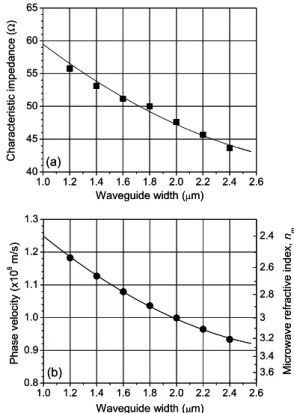
The width of the waveguide and the thickness of the un-doped layers, i.e. the MQW layer and the SCH layers, and the SI-InP cladding layer are important factors as regards controlling the waveguide capacitance so that the waveguide will satisfy the impedance matching and velocity matching requirements. Figure 2 shows the calculated characteristic impedance and the phase velocity as a function of optical waveguide width that we obtained using a commercially available high frequency structure simulator (HFSS). The dielectric constants used for the calculation are 12.4 for the semiconductor layers and 2.6 for the BCB. And the conduc-tivity value used for the n-InP layer is 4.2 × 10⁴S/m. The
conductivity value used for undoped core and SI-InP lay-ers is 0 S/m since these laylay-ers have sufficiently high resis-tance. As shown in Fig. 2(a), the 50-Ω impedance match-ing requirement will be satisfied when the width is around 1.8μm. And if we allow a margin of ±5 Ω, which corre-sponds to a−25-dB electrical reflection, the width tolerance is not severe, and ranges from 1.3 to 2.3μm.
As regards the velocity matching condition, the electri-cal bandwidth f0is given by
f0= 1.4c/(π|no− nm|)L
Fig. 2 Calculated characteristic impedance (a), and phase velocity (b) as a function of waveguide width.
where no and nm are the optical and the microwave e
ffec-tive refracffec-tive indices, respecffec-tively, L is the length of the E/O interaction section, and c is the free-space velocity of light [10]. As a relatively strong electric field is produced in the core region of the n-i-n waveguide, an L of only sev-eral millimeters is required, and we set L at 3 mm for our device. So, the allowable absolute difference between the optical and electrical indices needed to achieve a 40-GHz bandwidth is about 1.1. The no of our waveguide is about
3.7, and so nmshould fall into the 2.6 to 4.8 range. The
resulting nmderived from Fig. 2(b) shows that this value is
sufficiently large for our waveguide. From these calculated results and taking optical propagation loss and ease of fab-rication into consideration, we chose 2.0μm for the optical waveguide width.
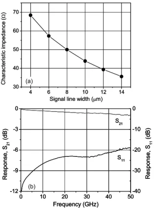
To facilitate connection with a differential output driver IC, the electrical input/output interface (GSG section) of the chip is placed on one side along the propagation axis. And we utilize microstrip lines (MSLs) from the GSG sections to the E/O interaction sections because they provide a small electrical loss, even when a bend has a small radius of curva-ture. This helps us to equalize the electrical length between the dual transmission lines in a small space. In other words, this contributes to keeping the chip small without requiring additional electrical phase adjustment. For our device, the radius is 50μm. Figure 1(c) shows a schematic cross-section of the MSL and its parameters. And Fig. 3(a) shows the calculated characteristic impedance against the signal line width of the MSL. We found that a width of 8μm provides
Fig. 3 Calculated characteristic impedance of the MSL as a function of signal line width (a), and measured S-parameters of the MSL part (b).
an impedance of 50Ω. And the impedance has a large tol-erance as regards the signal line width. We measured the electrical transmission (S21) and reflection (S11)
character-istics of the fabricated MSL part, which corresponds to a case where L= 0 mm (see Fig. 1(a)). We confirmed that there was very low electrical loss and reflection in the fre-quency range up to 50 GHz as shown in Fig. 3(b). So, our structure can very easily provide both impedance and ve-locity matching and it also has a large fabrication tolerance. By introducing these techniques, we fabricated an InP-MZ modulator chip with a size of only 4.5 × 0.8 mm.
3. Characteristics of MZ Modulator
First, we investigated the S-parameters of the fabricated chip itself by using GSGSG RF probes. As shown in Fig. 4 by the S21 curve, a 6-dB electrical-electrical (E/E) bandwidth
of 46 GHz was achieved. In addition, the reflection (S11)
was below−18 dB, which is sufficiently small for practical use. Note that the two electrodes exhibit good uniformity in terms of frequency response. These results prove that our n-i-n structure is suitable for obtaining a high-modulation bandwidth and 50-Ω impedance matching.
Then, the fabricated InP-MZ modulator chip is in-stalled in a compact package (21 mm (L)× 17 mm (W) × 8 mm (H)) whose footprint size is the same as those of con-ventional semiconductor laser modules [11]. Figure 5 shows a photograph of the modulator module. Two RF connectors for a differential electrical signal are placed on one side of
Fig. 5 Photograph of the dual-drive Mach-Zehnder modulator module.
Fig. 6 Small signal optical response of the modulator module.
the package. The module contains 50-Ω terminations and bias tees.
The required switching voltage when the extinction ra-tio (ER) was more than 15 dB was 2.2 V. The fiber-to-fiber insertion loss was 7 dB. As shown in Fig. 6, the measured small-signal 3-dB E/O bandwidth was 28 GHz, which is suf-ficiently large for the modulator to operate at 40 Gb/s.
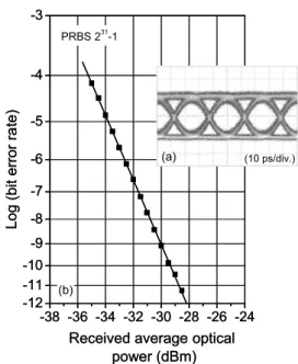
We then investigated the dynamic performance. A 40-Gb/s NRZ signal with a PRBS of 231−1 was applied to each
RF connector and the driving voltage for each port was only 1.3 Vpp. The operating wavelength was 1550 nm. Figure 7
shows the corresponding eye diagram and its bit-error-rate (BER) characteristics against the received average optical
Fig. 7 40-Gb/s NRZ eye diagram in a push-pull configuration with a driving voltage of 1.3 Vpp(a), and the back-to-back bit error rate (b).
power. Clear eye opening was obtained. The dynamic ex-tinction ratio (ER) was 10 dB. As shown in Fig. 7, we also confirmed error-free operation for a back-to-back configura-tion. These results indicate that our MZ modulator module has excellent characteristics, namely high-speed operation, a low driving voltage, and compactness.
We also investigated the 10-Gb/s optical DB transmis-sion characteristics of the modulator [12], [13]. The opti-cal DB format produces less spectral broadening than the conventional NRZ format and thus results in greater toler-ance to chromatic dispersion and narrow-band optical fil-tering. These features are beneficial for optical reconfig-urable add/drop multiplexing (ROADM) architecture with dense WDM (DWDM). As with many other advanced mod-ulation formats, the optical DB signal can be generated by a dual-drive MZ modulator driven in a push-pull configura-tion with a differential electrical signal whose amplitude is the half-wavelength voltage (Vπ). For such formats, the per-formance of the modulator including the resulting frequency chirp and the change in optical loss during modulation has a significant influence on the signal quality; therefore, this ex-periment is a good way to check the suitability of our mod-ulator for advanced modulation formats.
The three-level electrical signal for the DB signal was obtained from a 10-Gb/s NRZ signal (231 − 1
pseudoran-dom bit sequence) passed through a low-pass filter with a cut-off frequency of 2.8 GHz. The amplitude of the elec-trical signal was around 2.6 Vpp. The operating wavelength
was set at 1550 nm, and the average launched optical power into the SMF was+3 dBm. Then, the optical DB transmis-sion characteristics of signals traveling through 160, 200, and 240 km of SMF were investigated. The correspond-ing eye diagrams before and after transmission are shown in Fig. 8(a). We successfully obtained clear eye opening
Fig. 8 10-Gb/s optical duobinary eye diagrams and bit-error-rate charac-teristics of the module. (a) Eye diagrams for back-to-back, 160-km, 200-km, and 240-km transmissions. (b) Bit error rates.
even after a 200-km transmission. The BER measurements revealed that error-free operation was achieved for all dis-tances, and the power penalties were small, namely −1.0, 0.2, and 3.6 dB at BER= 10−12for transmission distances of 160, 200, and 240 km, respectively. The 160-km transmis-sion had a negative penalty because, with the DB signal, the cross point of the eye pattern for the back-to-back configura-tion is relatively high, and it becomes lower as the transmis-sion distance increases. Accordingly, this makes the sensi-tivity after transmission over a certain distance better than that with a back-to-back configuration. These results agree with previous reports and confirm that our modulator and an LN-MZ modulator have comparable levels of performance [13]. Moreover, our modulator is superior in terms of power consumption because of its low driving voltage. In addi-tion, the ample E/O bandwidth of our MZ modulator makes it possible to reduce the driving voltage further by lengthen-ing the E/O interaction sections, or to generate optical DB signals with a higher bit rate. Thus, we can also say that our modulator is useful for advanced modulation formats.
feedback (DFB) laser for our tunable transmitter module [16].
Figure 9 shows a photograph of the module. It consists of a TLA with a ten-DFB laser array, an n-i-n MZ mod-ulator, and a wavelength locker [17]. The TLA and the MZ modulator are mounted on the same metal carrier and a thermo-electric cooler (TEC). They are coupled by using lenses via an isolator. The optical output from the MZ mod-ulator is coupled into a fiber pigtail after passing through the wavelength locker, which is mounted on another TEC. All the lenses are welded by using a YAG laser to secure long-term stability and reliability. The module is 41 mm (L)× 13 mm (W)× 9 mm (H) in size, which is sufficiently small to realize a wavelength tunable transponder with a 300-pin SFF configuration.
Figure 10 shows the wavelength tuning characteristic of the module. The output wavelength can be tuned in a manner that selects an appropriate laser from the ten DFB lasers of the TLA, and then the temperature of the TLA chip is changed precisely over a range of 15 to 50 degrees as shown in Fig. 10(a). Our wavelength tunable transmit-ter covers wavelengths ranging from 1530 to 1562 nm. This
Fig. 9 Photograph and schematic drawing of the wavelength tunable transmitter module.
Fig. 10 Wavelength tuning characteristics and output spectrum of the module.
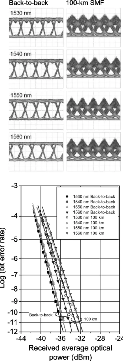
Fig. 12 BER performance at various wavelengths and eye diagrams for back-to-back and 100 km SMF transmissions.
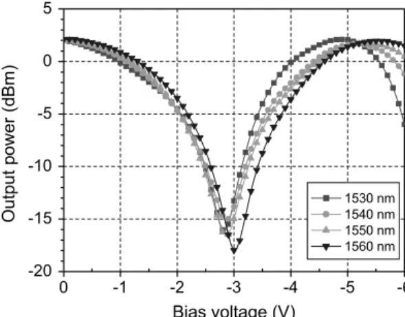
cess loss was obtained even at 2 Vπ(∼ 5 V). This is because the absorption edge of the waveguide core is sufficiently detuned from the operating wavelength. In other words, the linear electro-optic effect (Pockels effect) dominates the modulation in our modulator, and so the wavelength depen-dence and absorption caused by quantum-confined stark ef-fect (QCSE) can be reduced. The QCSE contribution to the modulation was estimated to be only one-fifth. Hence the n-i-n MZ modulator is very useful for our wavelength tunable transmitter.
Next, we demonstrate the dynamic performance of our transmitter module. The input electrical signal was a 10-Gb/s NRZ with a PRBS of 231− 1 for the wavelengths
de-Figure 12(b) shows the measured BERs for all wavelength channels. Error-free operation was confirmed. The sensitiv-ity penalties resulting from the transmission were less than 3 dB. Therefore, our wavelength transmitter module makes it possible to realize highly reliable, compact, and inexpen-sive 10-Gb/s wavelength tunable transponders with a low power consumption.
5. Conclusion
We developed a compact dual-drive traveling-wave elec-trode InP-based MZ modulator. The modulator has a novel n-i-n waveguide structure that assists the modulator to oper-ate at high speed and with a low driving voltage. The elec-trical input/output interface of the dual electrode is designed to be placed on one side of the chip to make it easy to con-nect with the differential driver ICs. We successfully used the fabricated modulator module in a push-pull configura-tion to generate a 40-Gb/s NRZ signal with a driving volt-age of only 1.3 Vpp. Furthermore, we also generated a
10-Gb/s optical duobinary signal using the module, and trans-mitted it successfully over a 240-km SMF. This verifies the applicability of our modulator to advanced modulation for-mats. In addition, we demonstrated a compact wavelength tunable transmitter, in which the n-i-n MZ modulator was co-packaged with the TLA. 10-Gb/s NRZ operation over the entire C-band was confirmed. We believe that our modulator is a promising candidate for compact, cost-effective wave-length tunable transponders with low power consumption.
References
[1] C. Rolland, R.S. Moore, F. Shepherd, and G. Hillier, “10 Gbit/s 1.56μm multiquantum well InP/InGaAsP Mach-Zehnder optical modulator,” Electron. Lett., vol.29, no.5, pp.471–472, 1993. [2] R. Spickermann, M.G. Peters, and N. Dagli, “A polarization
inde-pendent GaAs-AlGaAs electrooptic modulator,” J. Quantum Elec-tron., vol.32, no.5, pp.764–769, 1996.
[3] M. Fetterman, C.P. Chao, and S.R. Forrest, “Fabrication and analysis of high-contrast InGaAsP-InP Mach-Zehnder modulators for use at 1.55-μm wavelength,” IEEE Photonics Technol. Lett., vol.8, no.1, pp.69–71, 1996.
[4] L. Morl, C. Bornholdt, D. Hoffmann, K. Matzen, G.G. Mekonnen, and F.W. Reier, “A travelling wave electrode Mach-Zehnder 40 Gb/s demultiplexer based on strain compensated GaInAs/AlInAs tun-nelling barrier MQW structure,” IPRM98, WA3-4, 1998.
[5] K. Tsuzuki, T. Ishibashi, H. Yasaka, and Y. Tohmori, “Low driv-ing voltage 40 Gbit/s n-i-n Mach-Zehnder modulator fabricated on
[10] R.G. Walker, “High-speed III-V semiconductor intensity modula-tor,” IEEE J. Quantum Electron., vol.27, no.3, pp.654–667, 1991. [11] K. Tsuzuki, H. Kikuchi, E. Yamada, H. Yasaka, and T. Ishibashi,
“1.3-Vpp push-pull drive InP Mach-Zehnder modulator module for 40 Gbit/s operation,” ECOC 2005, Th2.6.3, pp.905–906, 2005. [12] T. Kurosaki, Y. Shibata, N. Kikuchi, K. Tsuzuki, W. Kobayashi, H.
Yasaka, and K. Kato, “200-km 10-Gbit/s optical duobinary trans-mission using an n-i-n InP Mach-Zehnder modulator,” IPRM2007, WeB1-3, 2007.
[13] A.J. Price, L. Pierre, R. Uhel, and V. Havard, “210 km repeater-less 10 Gb/s transmission experiment through nondispersion-shifted fiber using partial response scheme,” IEEE Photonics Technol. Lett., vol.7, no.10, pp.1219–1221, 1995.
[14] J.S. Barton, M.L. Masanovic, A.T. Pedretti, E.J. Skogen, and L.A. Coldren, “Monolithically-integrated 40 Gbit/s widely-tunable trans-mitter using series push-pull Mach-Zehnder modulator SOA and sampled-grating DBR laser,” OFC2005, OTuM3, 2005.
[15] R.A. Griffin, B. Pugh, J. Fraser, I.B. Betty, K. Anderson, G. Busico, C. Edge, and T. Simmons, “Compact, high power, MQW InP Mach-Zehnder transmitters with full-band tunability for 10 Gb/s DWDM,” ECOC2005, Th2.6.2, pp.903–904, 2005.
[16] H. Oohashi, Y. Shibata, H. Ishii, Y. Kawaguchi, Y. Kondo, Y. Yoshikuni, and Y. Tohmori, “46.9-nm wavelength-selectable arrayed DFB lasers with integrated MMI coupler and SOA,” IPRM2001, FBI-2, pp.575–578, 2001.
[17] K. Tsuzuki, N. Kikuchi, H. Sanjoh, Y. Shibata, K. Kasaya, H. Oohashi, H. Ishii, K. Kato, Y. Tohmori, and H. Yasaka, “Com-pact wavelength tunable laser module integrated with n-i-n structure Mach-Zehnder modulator,” ECOC2006, Tu3.4.3, pp.79–80, 2006.
Nobuhiro Kikuchi received B.E. and M.E. degrees in electrical and electronics engineering from Kobe University, Hyogo, Japan, in 1995 and 1998, respectively. In 1998 he joined NTT Opt-electronics Laboratories, and since 1999, he has been with NTT Photonics Laboratories and is engaged in research on optical semiconductor devices and their integrated devices for optical communication networks. He is currently a Re-search Engineer at NTT Photonics Laboratories. Mr. Kikuchi is a member of the Japan Society of Applied Physics.
Takeshi Kurosaki received the B.S. degree and M.S. degree in electronics engi-neering from Hokkaido University, Sapporo, Japan, in 1987 and 1989, respectively. In 1989, he joined the Opto-electronics Labora-tories, Nippon Telegraph and Telephone Cor-poration (NTT), Atsugi. Since then, he has been engaged in research on high-performance distributed-feedback (DFB) lasers and low-cost optical modules for optical transmission sys-tems. Mr. Kurosaki is a member of the Japan Society of Applied Physics.
Yasuo Shibata received B.E. and M.E. de-grees in electrical engineering from Keio Uni-versity, Kanagawa, Japan in 1985 and 1987, respectively. In 1987, he joined NTT Op-toelectronics Laboratories, Nippon Telegraph and Telephone Corporation (NTT), Kanagawa, Japan, where he has been engaged in research on optical switches, optical filters and integrated devices. He is currently with NTT Photon-ics Laboratories, and is engaged in research on SOAs, SOA-based functional devices and mod-ulators. He is a Senior Research Engineer in the Photonic Device Labora-tory of NTT Photonics Laboratories. Mr. Shibata is a member of the Japan Society of Applied Physics.
Hiroshi Yasaka received B.S. and M.S. degrees in physics from Kyushu University in 1983 and 1985, and was awarded a Ph.D. in Electronics Engineering from Hokkaido Univer-sity in 1993. In 1985 he joined Atsugi Electri-cal Communication Laboratories, Nippon Tele-graph and Telephone Corporation (NTT). Until 2008, he was engaged in the research and devel-opment of semiconductor photonic devices for optical fiber communication systems. In 2008 he joined the Research Institute of Electrical Communication (RIEC) at Tohoku University as a professor and has been engaging in research on highly functional semiconductor photonic devices and their monolithically integrated devices. Professor Yasaka is a member of the Japan Society of Applied Physics (JSAP).