High Mobility and Luminescent-Efficiency in Organic Single-Crystal
Light-Emitting Transistors**
By Satria Zulkarnaen Bisri*, Taishi Takenobu, Yohei Yomogida, Hidekazu Shimotani,
Takeshi Yamao, Shu Hotta and Yoshihiro Iwasa
Submitted to Adv. Funct. Mater. 2009, WILEY-VCH Verlag GmbH & Co.
KGaA, Weinheim.
For further information, link to the following URLs:
http://www.interscience.wiley.com/
Submitted to DOI: 10.1002/adfm.((please add manuscript number))
High Mobility and Luminescent-Efficiency in Organic Single-Crystal Light-Emitting Transistors**
By Satria Zulkarnaen Bisri*, Taishi Takenobu, Yohei Yomogida, Hidekazu Shimotani, Takeshi Yamao, Shu Hotta and Yoshihiro Iwasa
[*] S. Z. Bisri, Dr. T. Takenobu, Y. Yomogida, Dr. H. Shimotani, Prof. Y. Iwasa Institute for Materials Research, Tohoku University
Katahira, Aoba-ku, Sendai 980-8577 (Japan) E-mail: [email protected]
Dr. T. Takenobu
PRESTO, Japan Science and Technology Corporation Kawaguchi, Saitama 330-0012 (Japan)
Dr. H. Shimotani, Prof. Y. Iwasa
CREST, Japan Science and Technology Corporation Kawaguchi, Saitama 330-0012 (Japan)
Dr. T. Yamao, Prof. S. Hotta
Department of Macromolecular Science and Engineering, Kyoto Institute of Technology Matsugasaki, Sakyo-ku, Kyoto 606-8585 (Japan)
[**] We would like to acknowledge H. Nakanotani, Dr. M. Yahiro, Prof. C. Adachi (Kyushu University) for discussions concerning the experiments and results. This study was partly supported by Grants in Aid for Scientific Research (No. 17069003, 17204022,
18710091 and 17067009) from MEXT, Japan.
Keywords: Transistors, photonics, semiconducting oligomers, organic electronics, ambipolar semiconductors
We describe a high-performance ambipolar light-emitting transistor (LET) that has high hole- and electron-mobilities and excellent luminescence characteristics. Using this device, we observe a conspicuous light-confined edge-emission and current-density-dependent spectral evolution. These findings will result in broader utilization of device potential and they provide a promising route for realizing electrically driven organic lasers.
1. Introduction
Organic light-emitting transistors (LETs) [1] are of great scientific and technological interest. It provides unique planar-architecture that will be useful for probing fundamental optoelec-tronic properties of organic materials, i.e. charge injection, recombination and exciton forma-tion processes. The LET will open widespread novel device applicaforma-tions, such as
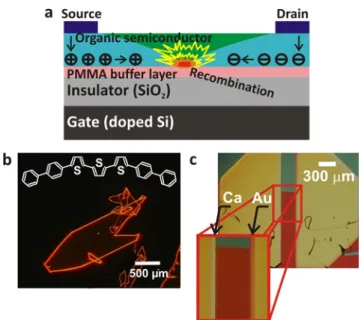
nano/microscale light source and highly-integrated organic optoelectronics. LET has a stan-dard metal-insulator-semiconductor field-effect transistor (MIS-FET) structure. The charge carriers are accumulated by gate voltages at the semiconductor/insulator interface and flow along that transistor channel. Recent development of interface engineering enables us to fabri-cate ambipolar FETs, where both electron and hole can be simultaneously transported. When holes and electrons are injected concurrently from source and drain electrodes, respectively, they recombine at the centre of the ambipolar LET channel (Fig. 1a). This device is inherently luminesce from transistor active materials.[2]
High-performance ambipolar LET requires a high exciton-density, which is deter-mined by both carrier-mobilities and luminescent-efficiency. However, it is still difficult to achieve in present organic semiconductor devices, since high mobility and high luminescent-efficiency are so far found to be mutually exclusive[3]. The compact molecular-crystal packing provides high mobility, but at the same time such compactness gives rise to the increasing non-radiative decay-paths for excitons, resulting in low luminescent-efficiency.[2,3a] To over-come this trade-off, multicomponent heterojunctions with different transport and luminescent layers have been exploited.[4] These structures were found to have modest mobilities (10-2 cm2 V-1 s-1), but the intercomponent reabsorption and the complicated interfacial processes might reduce device performance. In addition, their recombination zone was not well defined. On the other hand, single-component polymer[5] and small-molecule[1] thin-film LETs have been also studied. Recently, carrier mobilities of 10-2 cm2V-1 s-1 in a polymer LET has been
Submitted to ported by modifying the interface using ferroelectric buffer layer.[6] In spite of this, most of
the small-molecule thin-film LETs exhibited mobilities of less than 10-2 cm2 V-1 s-1.[1] Importantly, these mobilities were not intrinsic mobilities of the materials, but they were hampered by the grain boundaries. Latest finding showed that by removing the presence of grain boundary in highly-luminescent material of 1,3,6,8-tetraphenylpyrene (TPPy) led to significant improvement of carrier mobilities without any serious luminescent-efficiency drop. The hole mobility value was increased from around 10-5 cm2 V-1 s-1 in amorphous thin-film phase [7] to 10-2 or 10-1 cm2 V-1 s-1 in single-crystal phase.[8] In this context, we have taken a unique opportunity to investigate emission properties of high-luminescent single crystal on LET device configurations, by combining high mobility and luminescent efficiency, rendering the material prerequisite for an active material of the ambipolar LET devices.
α,ω-bis(biphenylyl)terthiophene (BP3T) exhibits luminescence efficiencies of up to 80 % in the single-crystal phase.[9] Several reports have demonstrated that BP3T can be used for LETs in a form amorphous thin-film ambipolar devices[10] and also single-crystal unipolar transistor devices; [11] the later one had hole mobilities up to the order of 10-1 cm2 V-1 s-1. BP3T crystals have been used to demonstrate photopumped amplified spontaneous emission (ASE) with a relatively low threshold energy of 8 μJ cm-2,[12] stimulated resonant Raman scattering (SRRS)[13] and cooperative-process super-fluorescence.[14] Moreover, the resulting emission exhibited self-waveguided edge-emission. It produced a well-defined photolumines-cence characteristic, in which light was confined within the crystal and only the fringes were strongly luminescent (Fig. 1b). Herein, we report a high-performance ambipolar LET that consists of BP3T single crystals. We demonstrated that the device had both high mobility and high luminescent-efficiency. Furthermore, it produced self-waveguided edge emission that is crucial for confining high-density of light emission, and a spectral narrowing by current in-crease was observed.
2. Results and Discussion
2.1 Ambipolar Field-Emitting Transistor of BP3T Single Crystals
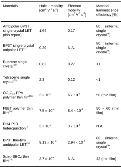
An FET based on a BP3T single crystal was fabricated using a well-established method for producing ambipolar organic single-crystal FETs.[8,15] Au and Ca asymmetric electrodes were used in order to promote better hole and electron injection (Fig. 1c). We considered the energy level matching between metal electrode work-function and BP3T single crystal HOMO and LUMO level. Typical ambipolar behavior was observed (Fig. 2a). Hole and elec-tron mobilities were found as high as 1.64 cm2 V-1 s-1 and 0.17 cm2 V-1 s-1, respectively, as deducted from the device transfer characteristics (Fig. 2b). The hole mobility in this device was higher than that reported for the other BP3T single-crystal LETs.[11,16] So far, the highest reported electron mobility in ambipolar single-crystal transistors was found to be around 0.3 cm2 V-1 s-1, which was in Rubrene single-crystal ambipolar FET.[13b] Therefore, the observed electron mobility in this BP3T device was reasonably high. The thin PMMA buffer layer in-serted between the BP3T and SiO2 layers was thought to promote electron transport.[17, 15a] Improved work-function matching of the electrodes[8,15b] and the air-free process (oxygen and moisture-free process) employed during device fabrication and measurement were considered as the contributing factors[18] for the high mobilities observation. However, electron suffered very high accumulation threshold voltage, which was around 160 V. It suggests that the carrier traps still remain at the BP3T/PMMA interface. PMMA purification and utilization of alternative buffer layer might reduce the threshold voltage, which later expected to increase the electron current inside the device.
The present findings of high carrier mobilities in an ambipolar BP3T device clearly defies the trend that high mobilities in organic semiconductors have been achieved only in materials with low luminescence efficiencies[2,3a] and vice versa. These mobilities were not only several orders of magnitude higher than those of other LETs made from thin films (either polymers[5] or small molecules[1]) and multi-component heterojunctions,[4] but they were also
Submitted to comparable to those of ambipolar single-crystal LETs made from tetracene[18] and rubrene[19]
(Table 1). Recently, there was a report about optimization of carrier mobility and optical gain
in polymer films by introducing more effective hopping sites.[3b] However, the obtained values are still two orders lower than these results. In amorphous or poly-crystalline thin films (either small molecule based or polymer based), the existence of grain boundaries signifi-cantly restricts the transport process besides the property of the molecules themselves, thus lowers the carrier mobilities. On the other hand, grain-boundary free organic-single-crystal would permit higher carrier mobilities. By using single crystals, we might increase the carrier mobilities of organic transistor without any surge of luminescent efficiency. These BP3T devices thus demonstrated that high-mobility ambipolar transport can be achieved in materials that have a high luminescent efficiency. Encouragingly, it opens the possibility of realizing ambipolar LETs based on highly luminescent single crystals, with current densities on the order of hundreds or thousands A cm-2, as performed by Rubrene and Tetracene [19] single-crystal LETs.
2.2 Self-Waveguided Edge Emission
In previous studies on ambipolar LETs,[5a-b,10,18] light emission was vertical to the substrate plane with the emission zone being a line parallel to the source and drain electrodes. By
contrast, in this present study, strong emission occurs solely at both edges of the BP3T crystal. The absence of surface emission in this device was clarified by using spectrometer, from which only noise level was detected. These emission characteristics are clearly depicted in
Fig. 3 and are consistent with those observed by photo-excitation.[9,12] The propagated
emis-sion along the wide crystal plane was detected by tilting the microscope, so that its axis became parallel with the crystal plane (Fig. 4). Figure 5 shows the side views of the device. As the drain voltages (VDS) were swept from -190 V to -230 V, the recombination (i.e. emis-sion) zone was shifted toward the source Au contact. The uppermost diagram schematically
depicts the recombination and subsequent emission. The emission zone shift is appropriately explained by carrier accumulation change by the applied voltage. At smaller value of drain voltages the recombination zone is located in the vicinity of the drain Ca electrode when holes are predominantly accumulated. The electrons are injected, but still not accumulated at the semiconductor/insulator interface, due to the accumulation threshold voltage. The recombina-tion zone moves from the Ca contact to the Au contact as electrons are gradually accumulated near the Ca contact with the further increasing voltage.This indicates typical recombination-zone spatial-behavior in ambipolar LETs[5a-b,10,18] (see Supplementary Video[20c]).
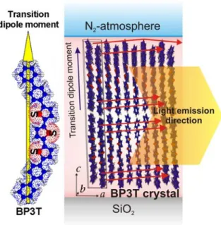
The edge emission may originate from a variety factors associated with molecular, crystal, and device structures (Fig. 6). From the molecular-orbital calculation of BP3T, the transition dipole moment was identified to be parallel to the molecular long axis.[21] Addition-ally, the molecules are stacked nearly perpendicular to the crystal ab-plane[22] as H-aggregate-like stacking. Consequently, the molecular emission inside the crystal tends to be emitted parallel to the crystal plane. The LET geometry is advantageous to the confinement of the light that diverge-emitted within small angles. It is because of the small tilting-angle of the molecules relative to the normal axis of the ab-plane,[22] together with the nearly upright configuration of the transition dipole moments (Fig. 6). The slab-stack waveguide structure of N2/single-crystal/SiO2, in which the BP3T single crystal acts as the core, causes any diverging light having a small grazing angle to be totally internal-reflected between the two slab-inter-faces. This structure prevents the emission leaking out from the crystal surface and makes it self-waveguided, so that it is eventually edge emitted. Henceforth, it gives a possibility to collect all of the recombination-produced light emission at very narrow single (or double) exits, which are the crystal (channel) edge.
From the refractive index viewpoint, the utilization of SiO2/Si substrate might induce light absorption by Si substrate. It has refractive index of 3.875,[23] which is higher than most
Submitted to of organic materials. It might also have significant high-dopant-density-induced absorption
coefficient. However, BP3T belongs to a class of materials so called Thiophene-Phenylene co-oligomers (TPCO), which possess a highly anisotropic optical behavior related with their molecules and molecular polarization orientations. Recent findings showed refractive index of 4.0 along c-axis direction in 1,4-bis(phenylthiophen-2-yl)benzene (AC5) single crystal.[24] It would imply that BP3T might have high refractive index, due to a stronger molecular dipole. We calculated the difference of transition dipole moments of BP3T and AC5 molecules by using single-excitation configuration interaction method with cc-pVDZ basis set (see Experimental). It was found that the molecular dipole of BP3T is 1.23 times stronger than AC5.Concurrently, this high refractive index would make the propagation losses of BP3T-cored waveguide minimum.
The prevailing edge emission and concomitant absence of surface emission ensured an extremely small optical loss within the crystal.[25] This is because of the
recombination-produced emission was confined inside the crystal and is effectively waveguided parallel to the device substrate. In this connection, Pauchard, et al.[26] remarked that losses introduced by the metal electrodes could be reduced by modifying the FET structure, since the transport of injected charge carriers is perpendicular to the optical confinement. Moreover, varying the channel width, which corresponds to the acting waveguide length, may increase the photon density of the edge emission. Thus, highly efficient edge emission is anticipated if the inher-ently small loss of the crystal is appropriately incorporated into the FET configuration.
The light would be emitted to all direction in the 2-dimensional crystal plane from its source in the recombination zone. Therefore, the edge emission itself is supposed to be observed from the whole crystal edge, with intensity maximum at the recombination zone. Most of the light that propagates toward electrodes might be absorbed by the metals. The other portion of light would still propagate to the all of the crystal edge along the channel, in
which the observed brightest spot indicated the proximity of the recombination zone point. Although this is very interesting issue, it is beyond the purpose of the present research. There-fore, future investigation on this aspect would be an important subject.
2.3 Electroluminescence Spectral Evolution
We prepared various configurations of BP3T ambipolar LETs that had different channel length and width variations. Those with wider channels tended to yield a higher photon den-sity emitted from the edge (Fig. 7). They were obtained by making positive utilization of the confinement effect, in addition to a slight increase in the operated current. The obtained electroluminescence (EL) spectrum has maximum peaks at 578 nm and 616 nm, which origi-nate from the 0-1 and 0-2 transitions of the BP3T single-crystal vibronic states,[14] respec-tively. This showed a good agreement with the single-crystal PL spectra (Fig. 8a). It is also in a similar manner to other single-crystal LETs,[19] in which emission peak consistency between PL and EL spectra were also observed. The relative peak intensity between these two bands were varied depending on each fabricated device (dashed line in Fig. 8a), particularly by the crystal dimensions. The light emission was found to be strongly unidirectionally plane-polar-ized to the crystal c-axis direction (Fig. 8b), corresponding to the TM polarization that attrib-uted to the upright transition dipole moment direction. This confined TM-mode propagation might be supportive to the ASE process.[14]
In several devices, we have observed a distinct spectral evolution that leads to spectral narrowing of the 578 nm peak due to drain current increase at the ambipolar regime (Fig. 9). The first three bottom lines show the spectra when the device still operated in saturation region of unipolar mode with different applied VDS. Here the drain current (ID) values were similar among those three spectra. The difference was laid on the number of immobile injected electrons, which was increased by the applied VDS. By the further increase of the VDS surpassing the electron accumulation threshold voltage, the device operated in an ambipolar
Submitted to manner. Here, the current flowing along the channel became the summation of both hole and
electron. The fourth spectrum line from the bottom indicates the initial emission profile after the device started to operate in the ambipolar mode. It shows a clear two-peaked spectrum that is similar to fig. 8a (orange dotted line). By further increase of the drain current (> 0.92 μA) in the ambipolar mode, the 578 nm peak evoluted to become narrower and sharper, as indicated by three uppermost spectral lines.
Recently, related spectrally-narrowed emissions has been reported from the substrate of organic light-emitting diodes with mechanisms ascribed to the cut-off mode[27] or leaky mode.[27] Another possible mechanism is amplified spontaneous-emission (ASE) or stimu-lated emission. Therefore, our results may be interpreted by one of the following two explana-tions: (i) the narrowed spectra in this BP3T ambipolar LET might be caused by a mechanism similar the one mentioned above (the cut-off mode or leaky mode); (ii) the current-density dependent spectral change is associated with an initial emission gain-narrowing mechanism. In this respect, we note that the aforementioned small optical loss possibly causes the spec-trally narrowed emissions, irrespective of what the origin of the emissions is (i.e., ASE or stimulated emission).[29] The self-waveguiding might prompt such emissions. However, the spectral narrowing mechanism in this device hasnot been identified yet. Among those three possible mechanisms, none of them is conclusive yet for explaining this finding. Therefore, a preliminary discussion and consideration for those mechanisms would be elucidated.
Firstly, we estimated the necessary current density needed for electrically-driven ASE in BP3T single crystal based on the photopumped ASE threshold energy of 8 μJ cm-2, excited by 337 nm pulsed UV excitation.[12] The estimated threshold current density is 10.3 kA cm-2. The calculation was taken place by accounting that the room temperature exciton lifetime of BP3T crystal is 1.68 ns.[9] However, the estimation of the threshold current density still neglected the possible threshold increase due to the metal electrodes, polarons, and exciton
annihilation. Also, we overlooked the possibility of threshold reduction due to the waveguide structure of LET and the Fabry-Perot cavity effect by the crystal-edge perfection. Next, we tried to calculate the current density of our BP3T LET device. We estimated the current den-sity for the observed electrically-driven spectral evolution (fig. 9), by approximating the charge carrier accumulation layer thickness of such device as thin as 1 nm.[5b,19] The spectrum line started to give a narrowing peak (at 578 nm) when the device surpass 229 A cm-2 current density operation. The maximum current density achieved in this measurement was 412 A cm-2 (the uppermost spectrum line). Hence, we found two-order difference between the opti-cally estimated ASE threshold current density and our observation in the ambipolar LET. Recently, it has been reported that threshold energy for photopumped spectral narrowing in BP3T single crystals is differs from one peak to another,[14] where one of them is independent with the excitation stripe length. Therefore, the ASE threshold energy might vary from device to device. Consequently, concurrent experiments of optical parameters should be done prior to each device fabrications.
Another possible mechanism of the observed current-driven spectral evolution is the narrowing via cut-off mode.[27] Here the peak wavelength was determined by a mode selec-tion that propagates along the interface due to perfect refracselec-tion. The wave-front that propa-gates along the interface would be possibly amplified, since partially it would interact with the organic molecules along the interface. This amplification has been identified to be also
current dependent in a supralinear manner.[27] Cutoff mode might be a way for reducing the energy threshold for spectral narrowing that lead to laser action. In this mechanism, the wave-length that is mode-selected as cutoff mode decided by the crystal thickness, the overall waveguide structure and the crystal refractive index. The cutoff wavelength seldom coincides with the molecular excitation peak. Therefore, investigation whether the observed spectral evolution directly correlates with the cutoff mechanism is necessary. However, the exact
Submitted to experimental refractive index value for the BP3T single crystal is still unknown. It is possible
that this class of materials (TPCO) might have some anomalously high refractive-index anisotropy.[14] Some indication from the molecular dipole calculation showed that BP3T has higher dipole moment compared with AC5 molecule (see experimental). This suggests possibility for BP3T crystal to have refractive index more than 4.0 in c-axis direction, since the transition dipole moment value is proportional to the refractive index.Therefore,
investigation on precise value of the refractive index is important to know the characteristic of the cutoff modes in this structure; furthermore, determine the spectral narrowing mechanism.
On the other hands, the possibility for having spectral narrowing via leaky mode might be overlooked. In this case, the narrowed spectrum is a result of optical modes that propagates out from the waveguide core into the subsequent layer and travels in that layer.[26,27b] In our BP3T transistor structure, such leaky mode will propagate into the SiO2 layer. The narrowing emission might come out from the interface of SiO2 and highly-doped Si substrate. However, such mode will suffer absorption by the substrate due to its metallic behavior. Moreover, findings on spectral narrowing via leaky mode showed independency from applied current in OLED structures.[28]
From discussion above, two possible mechanisms for the spectral narrowing, which are ASE and cutoff mode, are still open to explain our findings. In order to confirm the proper mechanism, further investigation is still being conducted. Nevertheless, those two mecha-nisms are promising paths for the realization of electrically-driven organic laser. Regardless the source of the electrically-induced spectral evolution in this device, it shows that ambipolar LET based on organic single crystal might be a promising route for the electrically-driven organic laser.
3. Conclusions
In conclusion, we have successfully demonstrated a high-performance ambipolar LET
containing organic single crystals that has both a high luminescence and high carrier mobility, which so far have been believed to be mutually exclusive. The bright emission achieved from this device is a result of the self-waveguided edge emission due to optical confinement inside the crystal. The current-induced spectral evolutions that were found in this experiments lead to a spectral-narrowing. These findings pave the way for ambipolar LETs based on organic single crystals to become a potential route for pursuing the realization of electrically driven laser oscillations from organic materials.[3a,30]
4. Experimental
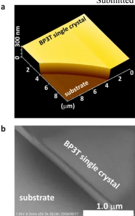
Single crystal growth: BP3T single crystals were grown from the synthesized powder [31] by means of a physical vapor transport method. The sublimation temperature of the source mate-rial was set at 365 oC and the temperature gradient at the crystallization zone was 3 oC cm-1 down to 270 oC. Ar gas, flew at 40 cm3 min-1, was used as transporting gas during the single crystal growth that lasted for approximately 36 h. After the crystal growth, the crystal-contained glass-tube was sealed and transported into an N2-filled glove-box, where crystal evacuation and further device fabrication processes were done, so there was no air and water moisture exposure to the crystals. Thin millimeter size platelets of single crystal were
obtained, with average thickness of 276 nm (measured by an atomic force microscopy – fig.
10a) and a clean edge morphology (indicated from scanning electron microscopy images – fig. 10b).
Device fabrication: The FET/LET device was fabricated in a bottom-gated, top-contact configuration [8,15]. A highly doped n-type Si wafer with a 500 nm thick SiO2 film was used as the device substrate, which acts also as the gate contact. A very thin (4-6 nm) Polymethylmethacrylate (PMMA) buffer layer was spin-coated on top of the substrates from
Submitted to toluene solution. The film was maintained overnight in an oven at 70 oC to remove the solvent,
and then annealed at 100 oC for 3 h in Ar atmosphere condition. The grown single crystals were subsequently laminated onto the substrate by utilizing the electrostatic force between the crystal and the substrate [32]. By considering the energy level matching between BPT
HOMO-LUMO levels (5.08 eV and 2.76 eV [12], respectively) and the metal work functions, Au (5.1 eV) and Ca (2.87 eV) were used as the top contact electrodes at opposite ends of the crystal. They were fabricated by evaporating Au on top of Ca through a shadow mask,
resulting Au/Ca bilayer with an offset. At one electrode, some part of Ca underlayer was kept to have direct contact with the single crystal to become electron-injector electrode. On the opposed electrode, the Au overlay film had a direct contact with the single crystal and it acted as hole injector electrode. Details on how the electrodes were fabricated have been explained in previous report [8].
Electric and optical characterization: The electrical and optical characterizations of the device were performed in the dark inside the glove box by means of a semiconductor parameter analyzer (Agilent E5207) and a CCD camera (Olympus CS230B) attached to an optical microscope (Keyence VH-Z100R). The microscope stage could be manipulated so that was able to be tilted to observe the light emission from the device edge, in addition to normal observation from the top of the device (Fig. 4). The images and videos of these characteriza-tions were captured on a computer and visualize by using Adobe Premiere TM CS3. The light-emission spectra were obtained by a Peltier-cooled CCD spectrometer (ORIEL FICSTM imag-ing spectrograph, model 77440), which is connected to the optical microscope through a fiber optic cable connection. The current dependent spectral evolution measurement was performed by measuring the spectrum in real-time with a 1 s time-domain accumulation windows on the spectrograph, while sweeping the drain voltage (VDS).
Theoretical calculations of molecular dipoles: All theoretical calculations were carried out with the Gaussian03TM package using single-excitation configuration interaction method with correlation-consistent polarized valence double-zeta (cc-pVDZ) basis set (CIS/cc-pVDZ method). The geometry of AC5 molecules was optimized with B3LYP hybrid density func-tional theory method employing cc-pVDZ basis set (B3LYP/cc-pVDZ). On the other hands, the geometry of BP3T molecules was taken from the X-ray crystallographic data (Cambridge Crystallographic Data Centre CCDC no. 232984). [22] Both molecules exhibited transition dipole moment direction that nearly parallel to the crystal c-axis. It was obtained that the dipole moment strength of BP3T and AC5 molecules are 2.5268 a.u. and 2.0508 a.u., respectively.
Received: ((will be filled in by the editorial staff)) Revised: ((will be filled in by the editorial staff))
Published online: ((will be filled in by the editorial staff))
_[1] A. Hepp, H. Heil, W. Weise, M. Ahles, R. Schmechel, H. von Seggern, Phys. Rev. Lett., 2003, 91, 157406.
_[2] M. Muccini, Nature Mater. 2006, 5, 605.
_[3] a) I.D.W. Samuel and G.A. Turnbull, Chem. Rev. 2007, 107, 1272; b) B.K. Yap, R. Xia, M. Campoy-Quiles, P.N. Savrinou, D.D.C. Bradley, Nature Mater. 2008, 7, 376. _[4] F. Dinelli, R. Capelli, M.A. Loi, M. Murgia, M. Muccini, A. Facchetti, T. J. Marks, Adv. Mater. 2006, 18, 1416.
_[5] a) J. Zaumseil, R. H. Friend, H. Sirringhaus, Nature Mater. 2006, 5, 69; b) J. Zaumseil, C. L. Donley, J. S. Kim, R. H. Friend, H. Sirringhaus, Adv. Mater. 2006, 18, 2708; c) J. S. Swensen, C. Soci, A. J. Heeger, Appl. Phys. Lett. 2005, 87, 253511.
Submitted to _[7] T. Oyamada, H. Uchiuzou, S. Akiyama, Y. Oku, N. Shimoji, K. Matsushige, H.
Sasabe, C. Adachi, J. Appl. Phys. 2005, 98, 074506.
_[8] S. Z. Bisri, T. Takahashi, T. Takenobu, M. Yahiro, C. Adachi, Y. Iwasa, Jpn J. Appl. Phys.2007, 46, L596.
_[9] S. Kanazawa, M. Ichikawa, T. Koyama, Y. Taniguchi, Chem. Phys. Chem 2006, 7, 1881.
_[10] K. Yamane, H. Yanagi, A. Sawamoto, S. Hotta, Appl. Phys. Lett. 2007, 90, 162108. _[11] K. Nakamura, M. Ichikawa, R. Fushiki, T. Kamikawa, M. Inoue, T. Koyama, Y. Taniguchi, Jpn J. Appl. Phys. 2005, 44, L1367.
_[12] M. Ichikawa, K. Nakamura, M. Inoue, H. Mishima, T. Haritani, R. Hibino, T. Koyama, Y. Taniguchi, Appl. Phys. Lett. 2005, 87, 221113.
_[13] H. Yanagi, A. Yoshiki, S. Hotta, S. Kobayashi, Appl. Phys. Lett. 2003, 83, 1941. _[14] T. Hiramatsu, N. Matsuoka, H. Yanagi, F. Sasaki, S. Hotta, Phys. Stat. Sol. C, 2009, 6, 338.
_[15] a) T. Takahashi, T. Takenobu, J. Takeya, Y. Iwasa, Appl. Phys. Lett. 2006, 88, 013507; b) T. Takenobu, T. Takahashi, J. Takeya, Y. Iwasa, Appl Phys. Lett. 2007, 90, 013507.
_[16] T. Yamao, T. Miki, H. Akagami, Y. Nishimoto, S. Ota, S. Hotta, Chem. Mater. 2007, 19, 3748.
_[17] L. L. Chua, J. Zaumseil, J. F. Chang, E.C.W. Ou, P.K.H. Ho, H. Sirringhaus, R. H. Friend, Nature 2005, 434, 194.
_[18] T. Takahashi, T. Takenobu, J. Takeya, Y. Iwasa, Adv. Funct. Mater. 2007, 17, 1623. _[19] T. Takenobu, S. Z. Bisri, T. Takahashi, M. Yahiro, C. Adachi, Y. Iwasa, Phys. Rev. Lett. 2008, 100, 066601.
_[20] a) http://www-lab.imr.tohoku.ac.jp/~satria/BP3T_LEFETmovie_S1.mov; b) http://www-lab.imr.tohoku.ac.jp/~satria/BP3T_LEFETmovie_S2.mov; c) http://www-lab.imr.tohoku.ac.jp/~satria/BP3T_LEFETmovie_S3.mov.
_[21] K. Bando, T. Nakamura, S. Fujiwara, Y. Masumoto, F> Sasaki, S. Kobayashi, Y. Shimoi, S. Hotta, Phys. Rev. B. 2008, 77, 045205.
_[22] S. Hotta, M. Goto, R. Azumi, M. Inoue, M. Ichikawa, Y. Taniguchi, Chem. Mater.
2004, 16, 237.
_[23] D. R. Lide (eds.), CRC Handbook of Chemistry and Physics, 2005.
_[24] T. Yamao, K. Yamamoto, Y. Taniguchi, T. Miki, S. Hotta, J. Appl. Phys. 2008, 103, 093115.
_[25] T. Yamao, K. Yamamoto, Y. Taniguchi, S. Hotta, Appl. Phys. Lett. 2007, 91, 201117. _[26] M. Pauchard, M. Vehse, J. Swensen, D. Moses, A. J. Heeger, E. Perzon, M. R.
Anderson, Appl. Phys. Lett. 2003, 83, 4488.
_[27] a) D. Yokoyama, H. Nakanotani, Y. Setoguchi, M. Moriwake, D. Ohnishi, M. Yahiro, C. Adachi, Jpn J. Appl. Phys. 2007, 46, L826; b) D. Yokoyama, M. Moriwake, C. Adachi, J. Appl. Phys. 2008, 103, 123104.
_[28] Y. Tian, Z. Q. Gan, Z. Q. Zhou, D. W. Lynch, J. Shinar, J. H. Kang, Q. H. Park, Appl. Phys. Lett. 2007, 91, 143504.
_[29] K. L. Shaklee and R. F. Leheny, Appl. Phys. Lett. 1971, 18, 475. _[30] M. A. Baldo, R. J. Holmes, S. R. Forrest, Phys. Rev. B 2002, 66, 750. _[31] S. Hotta, H. Kimura, S. A. Lee, T. Tamaki, J. Het. Chem. 2000, 37, 281. _[32] J. Takeya, T. Nishikawa, T. Takenobu, S. Kobayashi, Y. Iwasa, T. Mitani, C. Goldmann, C. Krellner, B. Batlogg, Appl. Phys. Lett. 2004, 85, 5078.
_[33] H. Nakanotani, S. Akiyama, D. Ohnishi, M. Moriwake, M. Yahiro, T. Yoshihara, S. Tobita, C. Adachi, Adv. Funct. Mater. 2007, 17, 2328.
Submitted to
Figure 1. a) Schematic diagram showing ambipolar light-emitting transistor operation, in
which holes and electron are independently injected from opposed electrodes; subsequently, they recombine within the conduction channel. b) Weak-excitation photoluminescence image of the utilized BP3T single crystal on PMMA/SiO2/Si substrate showing very bright edge emission corresponding to high photoluminescence efficiency of the crystal. c) An optical micrograph of the fabricated LET device with Au and Ca asymmetric electrodes (length (L) = 240 μm, width (W) = 1320 μm).
Figure 2. a) Plots of ID-VD FET output characteristics of BP3T single-crystal ambipolar device during p-channel (red lines) and n-channel operation (blue lines) for various applied gate voltages (VG). b)
Plot of
ID-VG transfer characteristics (blue squares) of the device during n-channel operation at drain voltage VD = 80 V, along with the corresponding ID1/2-VG plots (red circles), from which the carrier mobilities were extracted.
Submitted to
Figure 3. Edge emission of BP3T single-crystal ambipolar LET (length (L) = 80 μm, width
(W) = 860 μm), during ambipolar operation observed from the above of an identical device edges under ambient light conditions (see Supplementary videos[20a-b]). Light emission points are indicated by the two arrows.
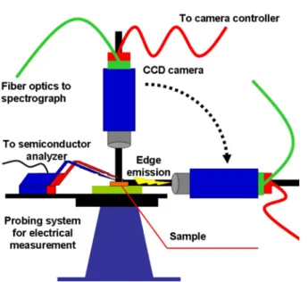
Figure 4. A schematic diagram of edge emission measurement apparatus showing embedded
electrical probing and optical measurement system, in which the microscope holder could be rotated.
Submitted to
Figure 5. Edge emission, observed from a horizontal direction, that move by drain voltages
(VD) sweep at ambipolar operation in BP3T single-crystal LET (length (L) = 240 μm, width (W) = 1320 μm) (see supplementary video[20c]). The bright side-view image of the single-crystal edge at the top of the figure is also given as reference.
Figure 6. A schematic illustration of the self-waveguided edge-emission mechanisms shows
that BP3T molecules stacked nearly perpendicular to the crystal plane, and their transition-dipole moments and molecular long-axis are parallel. Thus, causing the molecular light emission tends to be parallel to the crystal plane. The LET structure itself forms a BP3T-crystal-cored waveguide.
Figure 7. Light confinement effect on the edge-emission light density. Side views of the slab
BP3T single-crystal LETs. The device structure confined the light without any emission from the crystal surface and made all of the produced light propagate only to the crystal edge. Wider channel gives denser edge emission due to light confinement, in addition to the slightly operated-current increase caused by the short channel-length. The channel lengths
(horizontally defined) were 240 µm (left device) and 80 µm (right device). Note that the channel extends vertically out of the page, thus defining the channel width.
Submitted to
Figure 8. a) Comparison between electroluminescence (EL) spectra emitted from the device
and the corresponding photoluminescence (PL) spectra of the single crystal. Double-peaked EL spectra (orange dashed-lines) are related to the PL spectra with double peaks (green line), although the peak height relationship differs among devices (device I and II EL spectra). b) Optical polarization dependent of the EL spectra.
Figure 9. Current-dependent spectral evolution, measured in real-time, with 1-s time-domain
windows, during a drain voltage (VDS) sweep, leads to spectral narrowing at a high current regime with brighter emission observed from the device that has channel of 400 μm.
Submitted to
Figure 10. a) Atomic force microscopy (AFM) image of BP3T single crystal showing the
ickness of 276 nm. b) Scanning electron microscopy (SEM) image of BP3T single crystal th
edge showing a clear well-defined facet and smooth surface morphology, which giving advantage for the crystal as a gain resonator medium.
Table 1. Comparison of carrier mobilities and active-mater
cence efficiency
of BP3T single-crystal ambipolar LET device and other LETs
ial lumines
Materials Hole mobility [cm2 V-1 s-1] Electron mobility [cm2 V-1 s-1] Material luminescence efficiency [%] Ambipolar BP3T
single crystal LET (this report) 1.64 0.17 80 (internal, single crystal[9]) BP3T single crystal
unipolar LET[11] 0.29 N.A.
80 (internal, single crystal[9]) Rubrene single crystal[19] 0.82 0.27 <1 Tetracene single crystal[19] 2.3 0.12 <1 OC1C10-PPV
polymer thin film[5a] 3 × 10
-3 6 × 10⁻⁴ 50 (thin film) F8BT polymer thin film[5b] 7.5 × 10 -4 8.4 × 10⁻⁴ 50 ~ 60 (thin film) DH4-P13 heterojunction[4] 3 × 10 -2 3 × 10⁻² N.A. BP3T thin-film ambipolar LET[10] 9.13 × 10 -3 2.94 × 10⁻² 80 (internal, single crystal[9]) Spiro-SBCz thin film[33] 2.7 × 10 -4

![Figure 3. Edge emission of BP3T single-crystal ambipolar LET (length (L) = 80 μm, width (W) = 860 μm), during ambipolar operation observed from the above of an identical device edges under ambient light conditions (see Supplementary videos [20a-b] )](https://thumb-ap.123doks.com/thumbv2/123deta/8353785.1295673/20.892.281.617.122.639/emission-ambipolar-ambipolar-operation-observed-identical-conditions-supplementary.webp)
![Figure 5. Edge emission, observed from a horizontal direction, that move by drain voltages (V D ) sweep at ambipolar operation in BP3T single-crystal LET (length (L) = 240 μm, width (W) = 1320 μm) (see supplementary video [20c] )](https://thumb-ap.123doks.com/thumbv2/123deta/8353785.1295673/22.892.290.605.127.743/emission-observed-horizontal-direction-voltages-ambipolar-operation-supplementary.webp)