http://hdl.handle.net/2324/2236022
出版情報:Kyushu University, 2018, 博士(理学), 課程博士 バージョン:
権利関係:
transport and thermoelectric effects across ferromagnetic/nonmagnetic
metal hybrid nanostructures
Nagarjuna Asam
March 2019
Spin-caloritronics is a recent branch of spintronics where the interaction be- tween heat and spin is studied. While the discovery of spin Seebeck effect and thermal spin injection show a promise towards heat-to-spin conversion, ma- nipulation of spin current while using heat is also a possibility. With the ex- perimental demonstration of Spin-dependent Seebeck effect, spin-dependent Peltier effect, thermal Hall effects, anomalous Nernst effect, a lot of new in- teresting physics has come into limelight. Going forward, both development of new device geometries and clear understanding of the physics in the ex- isting devices is equally important. Particularly, there is a need to think beyond heat-to-spin-energy conversion alone. In this context, we studied a few other ways in which heat can interact with spin, leading to some new findings. In particular, we experimentally verified thermal analogues of three different spintronic effects.
First, we investigated the effect of a thermal gradient across a FM/NM/FM trilayer on the dynamics. By using the simple Joule heating from a W heater and measuring the Ferromagnetic Resonance (FMR) using Vector Network Analyzer (VNA), we systematically studied the dynamics under thermal spin injection caused by the thermal gradient. Here, beside the well-known damping-like spin transfer torque, we found new evidence for a field-like torque, resulting in a shift in the FMR frequency. Further, we found that the effect is pronounced when the top layer has smaller FMR dots instead of a large film, thereby showing a new way to improve spin injection efficiency by altering the geometry.
that a multitude of thermoelectric and thermal phenomena come into pic- ture simultaneously complicating the analysis. Keeping this in mind, we attempted to find further evidence for the co-existence of multiple thermo- electric effects. We took the well-studied nonlocal geometry of the thermal spin injection device and found that a part of the detected signal upon ther- mal spin injection has been left unexplained until now. Upon taking a closer look, we showed that the anomalous thermal Hall effect also comes into play simultaneously with the anomalous Nernst effect apart from the dominant thermal spin-dependent Seebeck effect.
In summary, various effects of temperature gradient across a FM/NM/FM trilayer, along a FM/NM/FM trilayer and a FM/NM interface in a non-local spin valve geometry have been shown. As a result, regarding dynamics, evidence for field-like and damping-like spin transfer torque and regarding heat flow, a thermal version of the GMR effect were shown. Additionally, in
Nernst effect, spin dependent Seebeck effect and anomalous thermal Hall was shown. In effect, experimental evidence for thermal spin transfer torque, thermal GMR and anomalous thermal Hall effect was found.
2.2 Spin-independent electron transport . . . 12
2.3 Electrical and thermal transport . . . 13
2.3.1 Thermo-electric effects . . . 15
2.4 Spin-dependent electron transport . . . 17
2.4.1 Anisotropic Magnetoresistance . . . 18
2.4.2 GMR . . . 18
2.4.3 Hall effects . . . 20
2.5 Magnetization dynamics . . . 22
2.5.1 Ferromagnetic resonance . . . 23
2.5.2 Spin-transfer torque . . . 25 3 Fabrication and measurement methods 28
1
3.1 Fabrication steps . . . 29
3.1.1 Lithography . . . 29
3.1.2 Deposition . . . 30
3.2 Measurement methods . . . 33
3.2.1 Vector Network Analyzer - Ferromagnetic Resonance . 33 3.2.2 Field-dependent lock-in measurement . . . 36
4 Experiment 1: Thermally driven spin transfer torque 38 4.1 Introduction . . . 38
4.2 Sample structure . . . 40
4.3 Experiment details . . . 44
4.4 Results and Discussion . . . 47
4.4.1 Dependence on dot-size . . . 55
4.5 Summary . . . 55
5 Experiment 2: Thermal Spin valve effect 56 5.1 Introduction . . . 56
5.2 Sample structure . . . 57
5.3 Experiment details . . . 60
5.4 Results and Discussion . . . 61
5.4.1 NiFe/Cu/NiFe . . . 61
5.4.2 Co/Cu/Co . . . 65
5.5 Summary . . . 69
6 Experiment 3: Anomalous thermal Hall effect 70 6.1 Introduction . . . 70
6.2 Sample structure . . . 72
2.1 Peltier effect . . . 15
2.2 Seebeck effect . . . 16
2.3 GMR in perpendicular-to-plane configuration . . . 19
2.4 Hall effect . . . 20
2.5 Anomalous Hall effect . . . 21
2.6 Magnetization dynamics under external magnetic field . . . . 23
2.7 Magnetization dynamics under spin transfer torque . . . 26
3.1 Joule evaporation/triple source e-beam evaporation setup . . . 31
3.2 DC/RF Sputter machine with several sources out of which we used Pt and W for the following experiments . . . 32
3.3 RF Sputter machine for SiO2 . . . 34
3.4 Vector Network Analyzer setup . . . 35
3.5 Lock-in measurement setup . . . 36
4.1 A schematic of the device . . . 41
4.2 Side view of the layers and their thickness . . . 42
4.3 Fabrications steps . . . 43
4.4 SEM image of the the device . . . 44 4
4.10 Parabolic fit of change in linewidth and frequency vs heater
current . . . 52
4.11 Heater current vs frequency shift for various NiFe dot sizes. We can see that smaller dots are causing better spin injection 53 4.12 A qualitative explanation of dot size dependence of spin in- jection efficiency. Apart from the spin current that is directly coming from below, NiFe dots also absorb a current from a radius of spin diffusion length in Cu around them. . . 54
5.1 A schematic of the device . . . 58
5.2 Fabrication steps . . . 59
5.3 Electrical GMR of NiFe/Cu/NiFe . . . 61
5.4 Seebeck Voltage at Pt2 of NiFe/Cu/NiFe device showing ther- mal GMR . . . 62
5.5 Result of COMSOL simulation showing a significant increase in the temperature . . . 63
5.6 Results of COMSOL simulation of NiFe/Cu/NiFe device and extraction ofκ . . . 64
5.7 Electrical GMR of Co/Cu/Co . . . 66
5.8 Seebeck Voltage at Pt2 of Co/Cu/Co device showing thermal GMR . . . 67
5.9 Results of COMSOL simulation of Co/Cu/Co device and ex- traction of κ . . . 68
6.1 A schematic of the device . . . 72
6.2 Fabrication steps . . . 73
6.3 Measurement configuration . . . 74
6.4 Thermal signal from device 1 . . . 75
6.5 Explanation of the interaction of three different effects in de- vice 1 . . . 77
6.6 Dependence on probe configuration . . . 79
6.7 Explanation of the signal in configuration B . . . 80
become more and more pronounced. Especially in nanoscale structures, heat generated because of Joule heating has become substantially large[1]. Pre- viously, all this heat energy has been thought of as an undesired waste of energy. But recently, several recent advances showed innovative ways to har- vest heat energy in nanoscale devices[2, 3, 4]. In this context, two important questions need to be asked. 1. How we can control and manipulate the flow of heat in nanoscale devices? 2. What are the various ways in which heat current can be used, especially in the context of electronic devices such as logic and memory?
Secondly, throughout the history of the computer, information storage almost always had something to do with magnetism. The first generation
7
computer, which dates back to times before the discovery of the transis- tor, used large magnetic drums[5] on which bits of information was stored.
These later got replaced by ring shaped magnetic cores[6] and as technol- ogy progressed[7], we reached the present state of tunnel-junction[8] based magnetic recording[9, 10] which are till-date the most popular as reliable non-volatile memory.
One of the most important breakthroughs in the evolution of computer memories is the discovery of GMR. By late 1980s, it was possible to epi- taxially grow high quality ultra-thin films[11] of magnetic materials. While studying the magnetic coupling of ferromagnetic thin films separated by a thin nonmagnetic layer, Albert Fert[12] and Peter Gr¨unberg[13] found inde- pendently that the resistance of the multi-layered structure depends on the relative magnetic orientation of the ferromagnetic layers. This simple obser- vation revolutionized how data is stored in computers and led to their joint Nobel prize for Physics in 2007[14].
The popularity of the GMR led to further exploration of the interface be- tween ferromagnetic(FM) and nonmagnetic(NM) materials. We now know that when a current is passed across a FM/NM interface, spin ‘accumula- tion’ happens at the interface even in the NM layer. That is, there will be a difference in up-spin and down-spin electron populations near the interface.
This difference in populations then diffuses inside the ferromagnet, causing a ‘spin current’ in steady state[15, 16]. Because the spins carry spin angular momentum, when the spin current encounters a ferromagnetic layer before
These concepts of GMR, spin current and spin-transfer-torque, along with several other new findings, together constitute the exciting field of spintron- ics, opening up new possibilities for low energy computing. Putting these two together namely the importance of heat transport and related effects in nanostructures and the new field of spintronics, we have a branch of spintron- ics called spin-caloritronics[20], where the interaction of electron spin angular momentum, heat and electrical current is studied.
Given that electrical and thermal current in metals are closely related to each other as we will see in detail in chapter 2, the idea is to experimentally verify the thermal analogues of three of the well known spintronic phenom- ena, which are 1. spin transfer torque, 2. Giant Magnetoresistance (GMR) and 3. Anomalous Hall effect
1.2 Outline of chapters
Chapter 1 gives a short introduction to this research. The importance of heat transport in nanoscale structures and the exciting new nature of the field of spintronics are discussed. Finally, the motivation for this research is shown.
Chapter 2 discusses the theory and background in detail. Starting from spin-independent electron transport, the first part of it shows the rela- tion between thermal and electrical transport and also spin-dependent elec- tron transport. In the second part, relevant spintronic phenomena such as Anisotropic magnetoresistance(AMR), Giant Magnetoresistance(GMR), Ferromagnetic Resonance(FMR), Anomalous Hall effect and spin-transfer- torque are discussed.
Chapter 3 shows the important fabrication and measurement methods involved. Under fabrication, the lithography and deposition processes are discussed in detail. The deposition tools used for this are also described.
Under measurement, Scanning Electron Microscopy for imaging, Vector Net- work Analyzer for measuring dynamics and lock-in measurement system are explained.
Chapter 4, Chapter 5, Chapter 6 are the chapters for three differ- ent experiments where thermal analogues are found experimentally for three corresponding spintronic phenomena.
show that the MR ratio is much higher in case of thermal GMR.
Chapter 6 is about thermal analogue of anomalous Hall effect. By us- ing this anomalous thermal Hall effect, we explain a previously unexplained asymmetry in the thermal spin injection signal in a lateral spin valve in non- local configuration.
Chapter 7shows a brief summary of the thesis.
Theory and background
2.1 Introduction
Electrons form the basis of the electrical transport. When it comes to met- als, electrons also are the dominant means of thermal transport[21], which is the flow of heat. Thus, to study electrical or thermal transport in metals, we need to understand the behaviour of electrons. The way electrons are arranged into energy levels almost solely determines the transport proper- ties. In this chapter, we will try to understand how this fundamental concept leads to several interesting implications.
2.2 Spin-independent electron transport
In one of the accepted theories of conduction in metals, the conduction electrons, which are from the outermost orbitals, are floating freely in a
12
level has a fundamental implication. That is, well below the Fermi level µ, transport cannot happen. Much above the Fermi level, there are no electrons available in the first place, so transport cannot happen. Therefore, much of the conductivity in the metals comes from electrons with energies near the Fermi level. The number of electrons flowing per unit time(number current) jn can be quantitatively expressed as
jn =−2e Z
dε
−∂f
∂ε
σ(ε)
1− ε−µ T ∇T
(2.1) Whereσ(ε) is number conductivity (which is electrical conductivity/electron charge) at the Fermi level.
2.3 Electrical and thermal transport
Since electrons carry electrical charge with them, the electrical current j is simply given by multiplying the number current jn with electron charge e−.
j =−ejn= 2e2 Z
dε
−∂f
∂ε
σ(ε)
1− ε−µ T ∇T
(2.2)
As for heat current, we can define heat current as the thermal energy carried by electrons. But electrons carry both thermal and chemical energy. There- fore, we can define thermal energy carried per unit time as the difference between total energy carried per unit time and the chemical energy carried per unit time.
jq =jε−µjn (2.3)
For a given energy level ε, this becomes
jqε= (ε−µ)jnε. (2.4) Substituting this in the equation 2.1, we have
jq =−2e Z
dε
−∂f
∂ε
σ(ε)
1− ε−µ T ∇T
(ε−µ) (2.5) Thus, in metals, thermal and electrical transport are closely related. We can combine the two into a matrix equation
j jq
=
L11 L12 L21 L22
E0
−∇T
(2.6)
where the matrix coefficients are given by[22]
L11 =σ (2.7)
L21 =T L12 =−π2
3e (kBT)2σ0 (2.8) L22 = π2
3 kB2T
e2 σ (2.9)
σ0 = ∂σ
∂ε (2.10)
The coefficients L11 and L22 are related by a factor of LT where L is the Lorenz number given by
L= π2 3
kB2
e2 (2.11)
where kB is the Boltzmann constant. This relation is known as Wiedemann- Franz law. Essentially, this says that at a given temperature, thermal con- ductivity κ is proportional to the electrical conductivityσ.
2.3.1 Thermo-electric effects
From the above section, we can also see that the a thermal gradient ∆T can cause an electrical current and an electrical field E can cause a heat current because both of them arise from the flow of electrons. This class of effects is known as thermoelectricity. The terms L12 and L21in the equation 2.6 correspond to the respective thermoelectric effects.
Peltier effect
Let us suppose we apply an electrical current j across a metal. The coefficient L21 means that a thermal currentjq is generated. As a result, at the end of the boundaries, heating/cooling can be observed. Mathematically,
Figure 2.2: Seebeck effect jq can be expressed as
jq = Πj (2.12)
where Π is known as Peltier coefficient, and is given by Π = L21
L11 (2.13)
Seebeck effect
On the other hand, if we apply a thermal gradient ∇T across a metal, it generates a heat current jq, which in turn generates electric fieldE across the metal. In an open circuit condition in steady state, this generates a corresponding voltage across the metal, which is known as Seebeck voltage.
The generated electric field E is related to the applied thermal gradient∇T by Seebeck coefficient S.
E =S∇T (2.14)
where S is given by
S = L12 L11
. (2.15)
2.4 Spin-dependent electron transport
In the equation 2.1, we used a factor of two that comes from Pauli’s exclusion principle, because both up-spin and down-spin electrons contribute to the current equally. However, if the conductivity of up-spin and down-spin electrons are different, we will have to re-write the expression for electrical current as
j↑/↓ =e2 Z
dε
−∂f
∂ε
σ↑/↓(ε)
1− ε−µ↑/↓
T ∇T
. (2.16) We need to note here that if up-spin electrons in one channel can somehow become down-spin electrons through some scattering mechanism, the above expression is not valid. This assumption is called two-current model[23], where the conductivity of the two spin channels is treated separately. Math- ematically, this is the same as having two parallel paths for electrical currents.
As we will see later, this can qualitatively explain a lot of the spintronic phe- nomena.
In ferromagnets where the population of up-spin and down-spin electrons are different, this will lead to several interesting observations.
2.4.1 Anisotropic Magnetoresistance
Anisotropic Magnetoresistance (AMR)[24, 25] is a phenomenon where the conductivity of a ferromagnetic material shows anisotropy. That is, the con- ductivity is dependent on the direction of the flow of electric current with respect to the easy-axis of the ferromagnetic material and the external mag- netic field.
2.4.2 GMR
In the years 1988-89, Fert[12] and [13] separately discovered that when thin layers of alternating ferromagnet(FM) and nonmagnetic metal(NM) are grown, the resistance of the whole structure depends on the relative magnetic orientation of the ferromagnets[26]. The simplest version of this would be a trilayer made up of FM/NM/FM. Since the change in resistance is substan- tially large, this phenomenon is called the Giant Magnetoresistance (GMR) and was used in computer memories[27] until it eventually led to the modern form of tunnel-junction based computer hard-disk drives. GMR is a direct result of spin-dependent conductivity.
current-perpendicular-to-plane
First, we will look at the case when current is flown perpendicular to the FM/NM/FM interfaces. This is known as current-perpendicular-to-plane (CPP) geometry. Figure 2.3 shows an illustration of how GMR works. Let us say r and R are the resistances for majority and minority spin channels respectively[28] and r << R. When the ferromagnetic layers are oriented parallel to each other, it means that one of the spin channels has resistivity r+r and the other hasR+R. The effective resistance RP will be
RP = (r+r)k(R+R) = 2rR
r+R ≈2r. (2.17)
In the anti-parallel case, both the spin channels have a resistance of r+R.
Therefore we have
RAP = (r+R)k(r+R) = r+R
2 ≈ R
2. (2.18)
Thus, the parallel and anti-parallel configurations have a large difference in resistance, leading to GMR. The Magnetoresistance(MR) ratio is given by
MR = RAP −RP
RP (2.19)
Figure 2.4: Hall effect
2.4.3 Hall effects
Hall effect is the direct result of a Lorentz force caused by a magnetic field on current carrying electrons in a conductor. When magnetic field is applied onto a current carrying conductor, the electrons are pushed in a direction perpendicular to the applied magnetic field and the current flow. Since the Lorentz force by a magnetic field B on an electron moving at a velocity vis given by
FMagnetic =−ev×B, (2.20)
the electrons are pushed in a direction same as that ofv×B. However, since electrons cannot flow continuously in the transverse direction, in steady state, this results in a measurable voltage perpendicular to the original current and the applied field. We can define the Hall coefficient RH as
RH = VHt
IB (2.21)
where I is the current flowing, VH is the measured Hall voltage and t is the thickness. The discovery of Hall effect[29] in 1879 in normal metals is a
Figure 2.5: Anomalous Hall effect
starting point for the subsequent several effects of similar fundamental origin in ferromagnetic metals. Hall effect can be used to make an efficient and inexpensive magnetic field sensor.
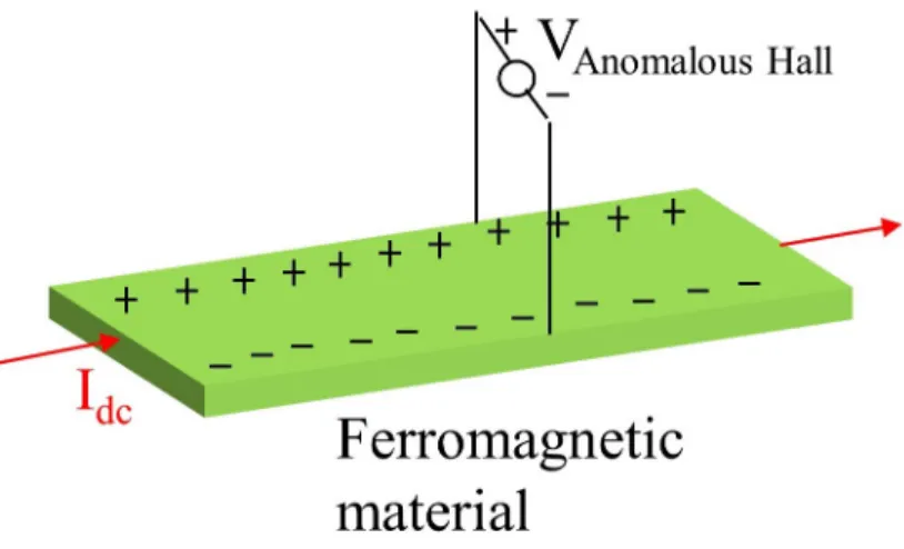
Anomalous Hall effect
Anomalous Hall effect is similar to Hall effect, but can be found in the absence of a magnetic field. When a current is flown through a ferromagnetic material, it is known that a Hall Voltage can be observed in the absence of external magnetic field[30]. However, the magnitude of this voltage is unusually large and the internal magnetic fields alone cannot account for this quantitatively. Nagaosa et al[31] have reviewed the phenomenon and identified three different causes. They are
1. Intrinsic deflection - arising from ‘Berry phase’[32]. The electrons flow- ing in a ferromagnetic material with nonzero Berry phase, intrinsically
have a velocity perpendicular to the applied electric field. This is known as ‘anomalous velocity’[33].
2. Spin dependent scattering - When the electron approaches an impurity, it experiences a scattering electric field which is dependent on spin. The two spins may be deflected in the opposite directions, which cause a transverse voltage. The asymmetric scattering can also be due to spin- orbit coupling.
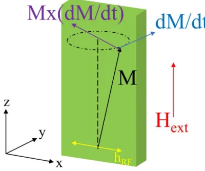
2.5 Magnetization dynamics
Let us define a local magnetic moment as the vectorM. The force experi- enced by the magnetic moment in an external magnetic field Hext influences it as
dM
dt =µ0γM×Heff (2.22)
where Heff is the effective magnetic field after accounting for the demagne- tizing field, γ is the gyromagnetic ratio given by
γ = ge
2mc (2.23)
whereg is the Lande g-factor, eis the charge of an electron, mis the mass of electron and c is the speed of light in vacuum. Since ddtM is perpendicular to M, it causes theMto precess around the magnetic field. However, similar to friction when mechanical motion is involved, there is a damping here which needs to be accounted for. After adding the damping factor, we arrive at the famous Landau-Lifshitz-Gilbert(LLG) equation.
dM
dt =µ0γ(M×Hef f)− α Ms
M× dM dt
(2.24)
Figure 2.6: Magnetization dynamics under external magnetic field where MS is the saturation magnetic field and α is the Gilbert damping factor. This form of LLG equation means that while the external magnetic field tends to cause precession around that magnetic field, the damping term causes the precession to dampen and disappear.
2.5.1 Ferromagnetic resonance
When we can somehow provide the local moments with an energy using a small oscillating magnetic field at radio frequency (RF) that can balance out the damping, the precession can happen indefinitely. This indefinite pre- cession is the largest when the frequency of applied RF field matches the natural frequency of precession. This phenomenon is called the ferromag-
netic resonance(FMR)[34, 35]. To get a quantitative understanding, let us say a constant field Hext = (0,0, h0) is applied along the easy axis of a fer- romagnetic cuboid of dimensions l×w×t where l >> w >> t as shown in figure 2.6. Let the applied RF magnetic field be hRF along the x-axis. The effective field will be given by
µ0Heff = (µ0hRF −Nxmx,−Nymy, µ0h0) (2.25) where Nx, Ny are the demagnetization factors where
Nx+Ny = 1 (2.26)
and the local magnetic moment M is given by
M= (mx, my, Ms). (2.27) Substituting these in the LLG equation 2.24, we get
∂
∂t −γ(µ0h0+NyMs)−α∂t∂ γ(µ0h0+NxMs) +α∂t∂ ∂t∂
mx
my
=−γMs
0
µ0hRF
.
(2.28) Upon Fourier transform, this becomes
−iω γ(µ0h0+NyMs) +iωα
γ(mx(µ0h0+NxMs))−iωα −iω
mx
my
=−γMs
0
µ0hRF
(2.29)
Finally, we derive the complex susceptibility tensor as
mx =χhRF (2.30)
ωx =γ(µ0h0+NxMs) (2.35)
ωy =γ(µ0h0+NyMs) (2.36)
ωM =γ(Ms) (2.37)
The χ0 and χ00 follow an anti-Lorentzian and Lorentzian shape respectively when plotted against the RF frequency ω. Since the imaginary part in the Fourier transform is proportional to the energy absorption, the S-parameter measured in chapter 3 will show a Lorentzian shape.
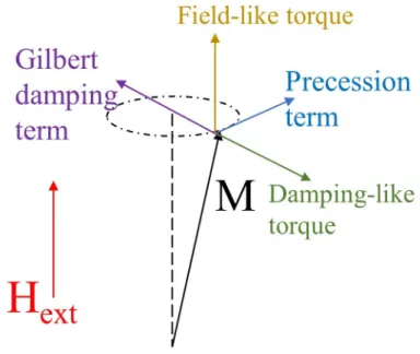
2.5.2 Spin-transfer torque
When spin current is passed into a ferromagnet, the spin angular momen- tum carried by the spin current gets transferred to the local moments and causes a torque. This is known as spin transfer torque[17, 36]. This spin transfer torque alters the dynamics defined by the LLG equation. Zhang, Levy and Fert[18] derived a mathematical expression for the influence of spin transfer torque on magnetization dynamics. However, we are modifying
Figure 2.7: Magnetization dynamics under spin transfer torque it slightly by considering Nx and Ny instead of ignoring the demagnetizing field along two of the axes. During the experiment in chapter 4, we found that Nx is low but not negligible. Zhang et al started by defining an interaction Hamiltonian
Hinteraction=−Jm·M (2.38)
Where m is the incoming magnetic moment. This is mathematically very similar to the energy of a magnetic moment in an external magnetic field.
Hlocal=−µ0Heff ·M (2.39)
Therefore, we assume that the LLG equation is modified as ifJmacts similar to applied magnetic field. Now, the modified LLG equation will be
dM
dt =µ0γ(M×(Heff +J m))− α Ms
M×dM dt
(2.40)
m⊥ = (0, msinθ,0) (2.42)
M= (sinφ,0,cosφ), (2.43)
where φ is the precession cone angle
m⊥ can be resolved along M,M×m,M×(M×m).
dM
dt =γ M× µ0Heff +J m2sin2θ
− α Ms
M×dM dt
+J m2sinθcosθsinφ (2.44) will be the final form of modified LLG. However, since the value of J is not theoretically derived, we replace the terms with a and b representing damping-like and field-like torque, respectively.
dM
dt =γ(M×(µ0Heff +b))− α Ms
M× dM dt
+aM×(M×m). (2.45) We need to note that although it seems like spin transfer torque is zero when the angle θ is zero, a small initial disturbance can cause precession, which increases the θ and creates a positive feedback loop. Thus, it is pos- sible to generate spin transfer torque although the injected spins are not at an angle to the local magnetic moment.
Fabrication and measurement methods
All the experiments discussed in this thesis involve fabrication of thin films of the order of a few nanometers and sub-micron patterning down to the level of a 100nm. Therefore, it is important to understand the fabrication process well to repeat the experiments reliably. Therefore, this chapter will show the details of fabrications steps. Additionally this chapter also presents the measurement methods involved which are Vector-Network-Analyzer(VNA) based Ferromagnetic Resonance (FMR), lock-in measurement technique for filtering the first of second harmonic of the output signal.
28
we spin-coat a chemical known as e-beam resist (as opposed to photoresist in optical lithography) which in our case is ZEP on the substrate and then bake it at 180◦C for solidifying.
Then, we subject it to electron-beam radiation only in the areas where a pattern is to be made. The exposure to the electron radiation makes the resist soft in the exposed area by changing its chemical property. Then, the sample is washed in O-Xylene, which reacts only with the softened part of the resist. This leaves the exposed area empty, surrounded by resist in the unexposed area. Please note that the thickness of the resist should be at least 10 times larger than the thickness of the thin film pattern to be made.
In our case, it was either 1µm or 3µm corresponding to a spin-coating speed of 5000rpm or 3000rpm respectively. Finally, we deposit the material on top of the pattern and then strip the resist using a remover which in our case is N,N Dimethyl Acetylamide ( also known as Z-Dimethyl Acetylamide or ZD- MAC). This stripping process only leaves the pattern on the sample where it is desired. This is commonly known as lift-off.
Exposure process
The instrument used was Elionix-7800, which allows an acceleration volt- age of 80kV and has a laser to accurately adjust the stage height. The pattern is made into a CAD file which is read by a computer. The e-beam which is accelerated to a high voltage is focused into a very narrow beam with diam- eter of about 2nm, and is controlled by the computer. The substrate is then exposed according to the pattern defined by the CAD file. The parameters that we need to take care of during the exposure process are
1. dosage - amount of electrons hitting unit area of the sample - the prop- erty of the resist determines how much dose is to be used, but subtle adjustments should be made according to the substrate and the pattern 2. chip size - the area of sample which is considered as a single unit and is exposed at a time - larger chip sizes can be used for larger patterns so that there is no breaking.
3. dot size - the machine treats the pattern as an aggregation of very tiny dots which are like pixels in an image - the finer the resolution, the sharper the pattern is.
3.1.2 Deposition
For deposition of metals, we used sputtering, e-beam evaporation or Joule evaporation techniques. Sputtering is the process of hitting the source with high energy Ar ions and making the source molecules jump off the surface.
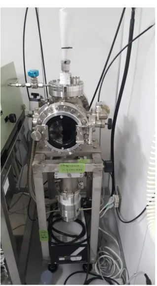
Figure 3.1: Joule evaporation/triple source e-beam evaporation setup Since this is performed at high-vacuum, the mean free path of the molecules is very large, and hence travel directly to the substrate and get deposited. Joule evaporation and e-beam evaporation are the techniques where the source is melted and evaporated by using Joule heating upon passing a very high cur- rent, or by hitting the source with an electron-beam. Again, it is done in a high vacuum to give the molecules a large mean free path.
Three machines were used for this purpose.
Joule evaporation + 3-source e-beam evaporation system
The essence of this system is to let us deposit the Ferromagnet/Nonmagnet heterostructures without breaking the vacuum. It also has a low-power ion- milling system inside it. It is powered by a cryo-pump and a turbo-mechanical
Figure 3.2: DC/RF Sputter machine with several sources out of which we used Pt and W for the following experiments
pump and can generate an ultra high vacuum of upto 1×10⁻⁷Pa. On the ferromagnet side, we can choose between CoFeAl, Co or NiFe as the sources, and Cu is deposited using the Joule evaporation system. As shown in figure 3.1, a magnet based sample moving system allows us to move the sample be- tween Cu and ferromagnet deposition areas without opening the door, thus maintaining the vacuum. There is a thickness monitor installed inside to measure the thickness of the deposited material with a precision of 1˚A.
Multi-Sputtering system
This machine has several DC and RF sputtering sources, and has a load- lock mechanism for achieving the vacuum very quickly. Out of these several sources, we used only Pt and W in the following experiments, whose depo-
The working mechanism is very similar to the above described multi-sputter system. It is important to note that to deposit insulators such as SiO2, we need to use RF because DC would cause a charge build-up and can create sparks and shorting.
3.2 Measurement methods
3.2.1 Vector Network Analyzer - Ferromagnetic Reso- nance
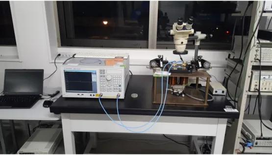
Vector Network Analyzer (VNA) is a tool that sends a low-power RF excitation across a 50Ω load, and measures the S-parameter as a function of the frequency. It can work from 300MHz to 20GHz and operates with a very low noise. This allows a sensitive measurement of Ferromagnetic Resonance (FMR). In our experiment, we fabricated a coplanar waveguide (CPW) made of Cu separated by SiO2 on top of the device, and connected the VNA port
Figure 3.3: RF Sputter machine for SiO2
Figure 3.4: Vector Network Analyzer setup
to the CPW. When a part of the device is undergoing FMR, as shown in the chapter 2, the S-parameter changes, thus causing a distinct Lorentzian peak in the frequency response of the VNA. This can be identified as the FMR and the linewidth and peak position can be accurately measured to understand the magnetization dynamics of the device.
However, when the impedance of the CPW is not perfectly 50Ω, then the frequency response of the VNA contains large additional background signal.
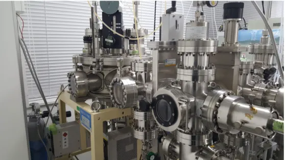
In order to remove this, we first measure the background signal at a given magnetic field, and then divide any signal with the background to remove it. Please note that we devide instead of subtract because the frequency re- sponse is measured in log scale. Figure 3.4 shows a picture of the VNA-FMR setup.
Figure 3.5: Lock-in measurement setup
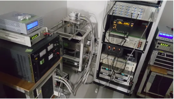
3.2.2 Field-dependent lock-in measurement
This setup was used to measure electrical and thermal spin injection sig- nals as well as thermal transport measurements. A picture of the setup is shown in figure 3.5. This setup has two closely spaced large electromagnets which are precisely controlled and calibrated to generate a desired magnetic field in between them. The device, which can have a maximum of 20 electri- cal connections is placed between the two electromagnets. Any current to be passed or voltage to be measured can be done using these electrical connec- tions. Please note that in order to use this, we need to place the device in a pre-designed chip and wire-bond the contact pads on the chip to the desired places on the device.
with a very high sensitivity. This is called lock-in measurement technique.
Experiment 1: Thermally driven spin transfer torque
4.1 Introduction
Spin current is the flow of spin angular momentum, which is said to act as an alternative for charge currents[37]. Since spin current carries spin an- gular momentum, this can be transferred to the local magnetic moments of a ferromagnetic material, causing what is known as spin-transfer-torque. Slon- czewski first proposed[17] in 1995 that spin transfer torque could be used for current-driven precession and switching phenomena in magnetic multilayers.
Berger[38] expanded this theory and predicted the modification of spin dy- namics, especially the Gilbert damping parameter. Tsoi et al[39] showed experimentally the effect of spin-transfer torque on magnetization dynamics, making the predictions of Berger[38] come true. There are several ways in which spin-transfer torque can be detected or put to practical use. The most
38
On the other hand, thermally driven spin injection has been observed ex- perimentally using several methods. Slachter et al[48] first showed a thermal spin injection into a nonmagnetic material from a ferromagnetic material.
Recently, we have seen that a new material CoFeAl can be used to efficiently generate thermal spin injection because of a special property of having op- posite signs of Seebeck coefficients for different spins[49, 50]. Combining the above two concepts of thermal spin injection and spin transfer torque, Hatami et al[51] predicted that magnetization switching can be achieved from thermally generated spin transfer torque. So far, Choi et al[52] have shown thermal spin transfer torque using ultrafast heat current generated by picosecond laser pulses. Bose et al[53] showed a change in the switching field, possibly caused by thermal spin transfer torque. Petit et al[54] have found a clear thermal signature in their analysis of the influence of electrical version of spin transfer torque on the magnetization dynamics, but did not take into account the possibility of thermally driven spin transfer torque.
Thus, a direct study of the influence of thermally driven spin transfer torque on the magnetization dynamics is in order. Therefore, taking advantage of
the CoFeAl developed in-house, we measured the influence of spin transfer torque generated by thermally injected spin current on the dynamics of NiFe nanodots.
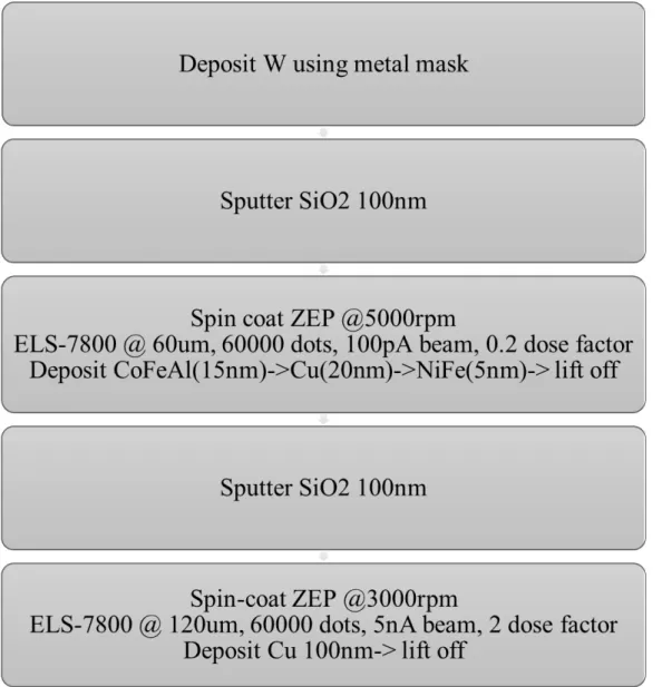
4.2 Sample structure
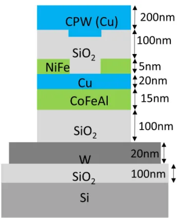
Figure 4.1 shows a schematic of the device. The central part of the device is the NiFe/Cu/CoFeAl trilayer, with thicknesses 20nm/15nm/10nm respec- tively. Figure 4.1 shows the side view of the device. The top NiFe layer is etched into numerous small dots of sizes ranging from 200nm × 400nm to 1 µm × 2µm, to improve spin injection efficiency. On top of the trilayer, there is a Co-planar Waveguide (CPW) made of 200nm thick Cu, separated by 100nm thick SiO2. The width and length of this CPW is chosen so that it covers the entire area of the trilayer. At the bottom, there is a W heating element, which is 20nm thick, to provide a resistance which is high enough for generating substantial thermal gradient from Joule heating.
Figure 4.3 shows the fabrication steps. The composition of NiFe is Ni:Fe in the ratio 80:20 as purchased. Since the CoFeAl source was made in-house, the composition of CoFeAl was measured using EDX and verified as Co:Fe:Al in the ratio 48:48:4.
Figure 4.1: A schematic of the device
Figure 4.2: Side view of the layers and their thickness
Figure 4.3: Fabrications steps
Figure 4.4: SEM image of the the device
4.3 Experiment details
As shown in figure 4.1, the measurement involves connecting a Vector Network Analyzer (VNA) to the CPW and measuring the single port RF scattering parameter S11across a range of frequencies from 300MHz to 16GHz as the output signal of the VNA. Similarly, we measured the signal at dif- ferent values of applied magnetic field, which was swept from -150mT to 150mT. Since the impedance of the CPW is not perfectly matched with the output impedance of the VNA, there will always be an impedance mismatch component in the frequency response. To eliminate it, we always first mea- sured the frequency response at a given field - say 200mT, which we call the background signal Sbg11 and divide the signal S11 at every field by the back- ground signal Sbg11. Please note that here we divided, not subtracted because
Figure 4.5: Typical signal measured by VNA and corresponding multi-peak fitting
Figure 4.6: Typical signal measured by VNA and corresponding multi-peak fitting
4.4 Results and Discussion
Firstly, we confirmed by COMSOL simulation by ensuring that there is sufficient temperature gradient across the device. As we can see in figure 4.7, the temperature gradient across the device CoFeAl/Cu/NiFe trilayer alone is 1.5mK across the 40nm thickness, which translates to a gradient of 37500K/m. When an RF current is passed through the CPW, it creates an RF electromagnetic Oersted field around it. And when the frequency matches the natural resonance frequency of the ferromagnet underneath, it causes ferromagnetic resonance (FMR). Since the energy for the FMR comes from the RF magnetic field generated by the CPW, and the S parameters of an RF circuit are inversely related to energy loss, the FMR is seen as an absorption peak in the FMR signal. Chapter 2 shows how this FMR signal is a Lorentzian peak. Figure 4.5 shows a typical S11 signal at a given mag- netic field (in this case 19mT). We can see two Lorentzian peaks, one each
Figure 4.7: Comsol simulation showing the temperature gradient across CoFeAl/Cu/NiFe trilayer in the inset
ω2 =γ2(µ0Hext+NxMs) (µ0Hext+NyMs) (4.1) where γ is gyro-magnetic ratio, H is the applied magnetic field, Ms is the saturation magnetization, Nx and Ny are anisotropy factors, under the con- straint Nx+Ny = 1. The directions of the axes x, y, z is defined as in figure 4.1. By fitting the Kittel equation to the graph of peak positions vs. applied field, we can estimate that the values of Nx, Ny, Ms are 0.023,0.977,0.97T for smaller peak and 0.006,0.994,1.58T for larger peak, respectively. Based on this, we can conclude that the smaller peak shown by red dots is from NiFe and that the larger peak shown by blue squares is from CoFeAl. This is consistent with the fact that the total energy absorbed by NiFe dots will be smaller because the total volume is smaller. We can take the error bars as 1σ confidence intervals of the peak fitting, which are not shown because they are smaller than the marker size.
Now, we passed a DC current through the W heating element and made the same measurement. Figure 4.8 shows how the FMR signal at a given applied field (33mT) varied with the DC current. We can see that the position of the CoFeAl peak is not changing as much, but the position of the NiFe
Figure 4.8: Heater current vs VNA signal
Figure 4.9: Heater current vs VNA signal zoomed in to NiFe peak
Figure 4.10: Parabolic fit of change in linewidth and frequency vs heater current
peak is shifting towards left as the heating current is increased. Figure 4.9 is a zoomed in version of figure 4.8, showing the left shift more clearly.
We plotted the the FMR frequency as a function of the heater current in figure 4.10, which shows a parabolic trend, owing to the fact that Joule heating is proportional to the I2 where I is the current. We also plotted the FMR linewidth vs. the heater current, which shows a similar parabolic trend. Again, the error bars in both the above graphs are the 1σ confidence intervals of the peak fitting.
According to Zhang, Levy and Fert[18], as discussed in chapter 2, the modified LLG equation is given by
dM
dt =γ(M×(Hext+b))− α Ms
M×dM dt
+aM×(M×m), (4.2) which means that the FMR will be modified as a change in both FMR fre-
Figure 4.11: Heater current vs frequency shift for various NiFe dot sizes. We can see that smaller dots are causing better spin injection
Figure 4.12: A qualitative explanation of dot size dependence of spin injection efficiency. Apart from the spin current that is directly coming from below, NiFe dots also absorb a current from a radius of spin diffusion length in Cu around them.
quency and linewidth, caused by field-like and damping-like torques respec- tively. The modified FMR frequency will be given by
ω2 =γ2(µ0Hext +b+NxMs) (µ0Hext+b+NyMs) (4.3) and the modified linewidth is given by
∆ω = ∆ω0−2γa (4.4)
Upon parabolic fit as shown in figure 4.10, we can extract the parameters a and b, and estimate the ratio of a/b to be approximately -2.5 at any given applied field. This indicates that the field-like torque is significant compared
spin current density is larger. Figure 4.11 shows how the change in fre- quency ∆ω depends on the dot size. This is consistent with our prediction that smaller dots improve the density of injected spin current.
4.5 Summary
In summary, we investigated the influence of thermally generated spin transfer torque on NiFe nanodots. We used external heating to generate thermal gradient across CoFeAl/Cu interface and produce this spin current which creates the subsequent spin transfer torque. The modification of fre- quency spectra in terms of both linewidth and resonance frequency point to the coexistence of both damping-like and field-like torque. Additionally, the dot size dependency shows the importance of geometry in such devices.
Experiment 2: Thermal Spin valve effect
5.1 Introduction
The discovery of Giant Magnetoresistance(GMR)[12, 13] is said to be a very important breakthrough in the field of computer memories. In addition to being used as a memory cell[55], GMR based devices could also be used as magnetic read-heads[56], isolation devices[57] and magnetic field sensors[58].
More recently, GMR was employed in bio-sensor applications[59, 60]. Over the course of time, significant advances were made in the field of spintronics and devices such as lateral spin valve[61] became popular. A new branch of spintronics known as spin-caloritronics, where the interaction between spin and heat is studied, recently became an active area of research[20]. The dis- covery of the spin Seebeck effect[62] started a wave of research into this field.
Very soon, several new effects such as spin-dependent Seebeck effect[63, 48], 56
have reported field-dependent thermal conductivity in magnetic multilay- ers. However, a quantitative comparison of thermal and electrical versions of GMR still needs to be done. Additionally, because of the large size, the presence of domains in their samples complicates the analysis and prevents us from making any implications about Wiedemann-Franz law. Recently Bakker et al[1] have developed a useful technique to study the heat trans- port in nanowires. Using this method, we studied the heat transport in GMR nanowires upon Joule heating by Pt wires and detection using Seebeck effect.
5.2 Sample structure
A schematic of the device is shown in figure 5.1. The object of study is a long, thin GMR wire, 400nm thick and 2µm long made of Ferromag- net(FM)/Nonmagnet(NM)/Ferromagnet(FM) trilayer. The NM was always Cu, but the FM was either Co or NiFe. This was made on a SiO2/Si sub- strate. On the GMR wire, we made long vertical bars of Pt which are 20nm
Figure 5.1: A schematic of the device
thin and 400nm wide. The Pt wire both acts as a heating element and a ther- mometer by forming a thermocouple with the GMR wire. The gap between two Pt wires is 400nm.
• Device 1: The GMR wire is made of NiFe/Cu/NiFe of thicknesses 15nm/20nm/5nm respectively. The SiO2layer in the substrate is 100nm thick. The NiFe is Ni:Fe in the ratio 80:20.
• Device 2: The GMR wire is made of Co/Cu/Co of thicknesses 20nm/10nm/10nm respectively. The SiO2 layer in the substrate is 1µm thick.
Figure 5.2: Fabrication steps
Figure 5.2 shows the fabrication steps.
5.3 Experiment details
First, we measured the electrical GMR by passing low frequency AC cur- rent between Pt1 and Pt4 and measuring the lock-in voltage between Pt2 and Pt3.
After measuring the electrical GMR, a low frequency AC current of fre- quency 173Hz is passed through the Pt1 wire. This causes Joule heating in the Pt1 wire, which generates a horizontal thermal gradient across the GMR wire. The heat flow through the GMR wire, which is dependent on the ther- mal conductivity, creates a small additional temperature at the junctions of Pt2,Pt3 and Pt4 with the GMR wire. Then, we measured the second har- monic of the voltage generated at Pt2, Pt3 and Pt4. Since Joule heating is proportional to the square of the current flowing through the Pt1 wire, the effect of Joule heating will be seen as a second harmonic. By separating the second harmonic using lock-in measurement, we can eliminate the possible spurious non-thermal contributions.
We do this procedure for both device 1 and device 2. All measurements were performed at room temperature.
Figure 5.3: Electrical GMR of NiFe/Cu/NiFe
5.4 Results and Discussion
5.4.1 NiFe/Cu/NiFe
Figure 5.3 shows the electrical GMR. Because of the difference in thick- nesses, the top layer and the bottom layer switch at different magnetic fields.
Thus, we can see different resistances for parallel and anti-parallel magneti- zation configurations. From this, we can calculate the electrical GMR from the expression
GMR = RAP −RP
RP (5.1)
Figure 5.4: Seebeck Voltage at Pt2 of NiFe/Cu/NiFe device showing thermal GMR
the temperature
as 0.3%. Figure 5.4 shows the Seebeck voltage measured at the terminal Pt2 upon flowing Joule heating current through Pt1. We can see that this too shows a qualitatively similar switching to that of the electrical version. The switching fields show similar values to that of electrical GMR. For a quan- titative estimate of the thermal conductivity κ, we have the same problem as that of the above. In addition to the above discussed problem of l, there is also a significant amount of heat draining into the substrate. To take ac- count of all of these, we use the same approach using simulation results from COMSOL Multiphysics software.
Figure 5.5 shows the temperature distribution arising from Joule heating.
Please note that we have set the temperature at the bottom of the substrate to be always at room temperature and also used a smaller substrate of the same thickness. This is to avoid the computing time of several days. From the simulation, we plotted the estimated additional temperature ∆TPt2 in
Figure 5.6: Results of COMSOL simulation of NiFe/Cu/NiFe device and extraction of κ
ratio to be approximately 4.3%, which is much higher than the electrical GMR.
5.4.2 Co/Cu/Co
In device 2, the NiFe/Cu/NiFe was changed to Co/Cu/Co because the latter was known to generate large GMR ratio arising from stronger spin- dependent scattering at the interface[73]
Figure 5.7 shows the electrical GMR for Co/Cu/Co. Using the average values of RP and RAP we can calculate the GMR ratio from equation 5.1 as
≈1%. As expected, this is a significant improvement from NiFe/Cu/NiFe.
Figure 5.8 shows the Seebeck voltage at the Pt2 for device 2. Again, there was a clear difference between parallel and anti-parallel configurations. More importantly, using a thicker SiO2 resulted in a much higher base voltageS0, thereby enabling better signal to noise ratio. The plot of κ vs ∆T is shown in figure 5.9. The values of κP and κAP were found to be 58.9Wm−1K−2 and
Figure 5.7: Electrical GMR of Co/Cu/Co
Figure 5.8: Seebeck Voltage at Pt2 of Co/Cu/Co device showing thermal GMR
Figure 5.9: Results of COMSOL simulation of Co/Cu/Co device and extrac- tion of κ
using a new nanoscale heat sensing technique using Seebeck effect. We used NiFe/Cu/NiFe and Co/Cu/Co nanowires, both of which showed clear mag- netoresistance in thermal and electrical signals. By combining this with numerical estimate from COMSOL simulations, we were able to obtain the values of magnetoresistance for electrical and thermal transports. Surpris- ingly, we found that the thermal conductivity shows a much larger MR ratio than the electrical GMR.
Experiment 3: Anomalous thermal Hall effect
6.1 Introduction
The discovery of Hall effect[29] in 1879 in normal metals is a starting point for the subsequent several effects of similar fundamental origin in fer- romagnetic metals. Anomalous Hall effect[30] which was discovered by Hall himself two years later, received new attention after 100 years[74, 31] since nanoscale devices became ubiquitous and measurement methods were mod- ernized. Falling into the same class of effects are spin Hall effect[75, 76, 77], spin injection Hall effect[78], quantum spin Hall effect[79, 80] and so on.
Spin-caloritronics is a new branch of spintronics in which the interaction between spin and heat is studied[20]. One of the hot areas of research in spin-caloritronics is discovery of various thermoelectric versions of the above
70
tric effects, the thermal(heat current) version of Hall effects has also been researched. Thermal Hall effect was shown in Copper[88], and anomalous thermal hall effect was shown in anti-ferromagnetic MnSn3 by Li et al[89]
and in potassium by Tausch et al[90]. In the light of renewed interest in spin-caloritronic Hall effects, Xu et al[91] theoretically predicted anomalous thermal Hall effect in ferromagnets.
Lateral spin valve[61] in a non-local configuration[92, 41] is a way to gen- erate pure spin current in metallic nanostructures. Using the same device structure, thermally driven spin injection[48] is made possible. However, even here additional contribution from the interplay of Seebeck effect and Peltier effect is observed as a background signal[93]. Furthermore, anoma- lous Nernst effect has been shown to cause an asymmetry[94, 95] in the ther- mal spin injection signal. Using the new material CoFeAl which generates a large thermal spin valve signal[49], we made a lateral spin valve to care- fully study the interplay of different spin-caloritronic effects in the non-local configuration.
Figure 6.1: A schematic of the device
6.2 Sample structure
Figure 6.1 shows a schematic of the device. The geometry of the device is the same as that of the standard local spin valve that has been previously optimized. [49, 50]. There are two long, thin vertical bars of a CoFeAl(CFA) of thickness either 20nm or 50nm and width 100nm, which are joined by a 200nm thick, 100nm wide Cu channel. The large Cu thickness is to generate a larger thermal gradient across Cu/CoFeAl junction. The center-to-center distance of the two CoFeAl bars was 300nm, which is substantially smaller than the spin diffusion length in Cu. The coercivity of one of the CoFeAl bars was changed by changing the shape. Two small pads are added at the ends, which makes the switching easier, therefore the switching field was smaller.
The fabrication steps are shown in the figure 6.2
Figure 6.2: Fabrication steps
Figure 6.3: Measurement configuration
6.3 Measurement
Figure 6.3 shows the measurement technique. In this experiment, to generate pure spin current, non-local measurement method was employed.
Current Iin is flown between terminals A and B as shown in the figure and voltage Vout is measured between terminals C and D. Thus, CFA1 becomes the injector and CFA2 becomes the detector. Now, we used lock-in measure- ment and measured the first harmonic(1ω) of the Vout for the conventional electrical measurement and the second harmonic(2ω) for thermal signal. The fact that Joule heating is proportional to Iin2 causes the thermal signal to ap-
Figure 6.4: Thermal signal from device 1
pear as the second harmonic.
6.4 Results and discussion
Initially, we made the device with a CoFeAl thickness of 20nm. We con- firmed that the device behaved as expected by measuring the electrical spin injection signal as the first harmonic of Vout. Then, we measured the second harmonic signal, which showed a thermal signal as expected. This is shown in figure 6.4. There are two predominant contributions to this signal. First is the spin-valve-like switching which comes from the thermal spin injection from CFA1 and detection at CFA2. Second is the background signal VSeebeck that comes from the heat that is generated at the injector and then flows
through the Copper channel to CFA2, which ultimately generates Seebeck voltage between CFA2 and Cu.
But, these two effects alone cannot explain the asymmetry. This asym- metry is supposed to be caused by the anomalous Nernst effect. Anomalous Nernst effect is the thermoelectric effect in ferromagnets where a thermal gradient produces a perpendicular voltage. This is the thermoelectric ana- log of Hall effect and has similar origins. Since the heat flow at Cu/CFA2 interface is mainly vertical and CFA2 is a ferromagnet, there was a small voltage created perpendicular because of the anomalous Nernst effect. And because the voltage generated depends on the magnetization of the CFA2, this caused an asymmetry in the thermal signal.
However, this picture is not complete. Let us call the differences in volt- age whenever there is a magnetization reversal(switching) as ∆V1, ∆V2, ∆V3 and ∆V4 as shown in figure 6.4. The switching at a higher field ∆V2 and
∆V4 are caused by the switching of CFA2, which is the detector. But ∆V1 and ∆V3 are caused by switching at the injector CFA1. Hence, the difference
∆V1−∆V3 cannot be explained by the anomalous Nernst effect.
In order to explain this, we looked at the geometry of the spin-valve de- vice more closely. As shown in figure 6.5, the Cu channel surrounds the CoFeAl bar because of the fabrication process. Although the dominant ther- mal gradient ∆Tz is vertical (along z-axis) because of the large Cu channel, anomalous thermal Hall effect causes a small lateral heat current. This lat-
Figure 6.5: Explanation of the interaction of three different effects in device 1
eral heat current then contributes to the background signal VSeebeck. Since the anomalous thermal hall effect also depends on the magnetization direc- tion of the ferromagnet, a switch in CFA1 induces change in VSeebeck. This causes a difference between ∆V1 and ∆V3, thus completing the picture. Fig- ure 6.5 explains qualitatively how the interplay of three signals (1) thermal spin injection, (2) anomalous Nernst effect and (3) anomalous thermal Hall effect result in the overall signal that we measured.
6.4.1 Upon reversing the roles of injector and detector
To measure the thermal hall effect more clearly, we needed to enhance the sideways contribution to the overall signal. Hence, we made a new device with a thicker CoFeAl of 50nm. We repeated the above process and found that the asymmetry was even more pronounced.
After getting a clearer signal, we did the experiment once again with the injector and detector reversed. That is, currentIinwas flowed through CFA2 and voltage was detected at CFA1. As expected, this causes a change in the second harmonic lock-in signal as shown in figure 6.6. Let us call the injector-detector configurations in figure 6.6 as P and Q respectively. In both configurationsP and Q, asymmetries were observed as ∆V1 <∆V3 and
∆V2 < ∆V4. However, the magnitude of asymmetry is different between P and Q. In configurationP, ∆V3−∆V1 is caused by anomalous thermal Hall effect and ∆V4−∆V1 by anomalous Nernst effect. In configurationQ, ∆V4−
∆V2 is caused by anomalous thermal Hall effect and ∆V3−∆V1 is caused by
Figure 6.6: Dependence on probe configuration
Figure 6.7: Explanation of the signal in configuration B
configuration. After a detailed analysis of the signal with enhanced sideways contribution, we concluded that the asymmetry is caused by the combina- tion of anomalous Nernst effect and anomalous thermal Hall effect. This shows the importance of careful understanding of Hall-effect like signals in nanoscale thermal transport.
Summary
To summarize, we experimentally verified the thermal analogues of three different spintronic effects, namely spin transfer torque, Giant Magnetoresis- tance(GMR) and Anomalous Hall effect.
First, we investigated the effect of thermally generated spin transfer torque on NiFe nanodots. For this purpose, we used a trilayer made of NiFe/Cu/CoFeAl. The top NiFe layer was patterned into small dots for spin injection efficiency. We used a W heater to create a vertical thermal gradi- ent and a Cu co-planar waveguide to measure the ferromagnetic resonance (FMR) using vector network analyzer (VNA). The VNA-FMR signal shows a clear dependence of dynamics on the thermal spin injection, implying evi- dence for spin transfer torque. We found that both linewidth and resonance frequency are altered, which means that both damping-like torque and field- like torque are present.
82
lateral spin valves in the nonlocal configuration. We found that the interplay of anomalous Nernst effect and the anomalous thermal Hall effect is the rea- son for the asymmetry.
In all, we studied various effects of temperature gradient across ferromag- net/nonmagnet heterostructures and found experimental evidence for ther- mal spin transfer torque, thermal GMR and anomalous thermal Hall effect.
Given the newly found importance of spin-caloritronics and the renewed focus on heat-to-spin conversion techniques, a good understanding of the link between thermal and electrical transport mechanisms is necessary. Putting the above research next to a good amount of existing evidence for thermo- electric analogues of spintronic effects, as long as we don’t go ’quantum’, we can conclusively say that any new finding in electrical transport can be ex- pected to be replicated in the thermal and thermoelectric versions and vice versa.
[1] F. L. Bakker, J. Flipse, and B. J. Van Wees, “Nanoscale temperature sensing using the Seebeck effect,” Journal of Applied Physics, vol. 111, no. 8, 2012.
[2] G. Chen and A. Shakouri, “Heat Transfer in Nanostructures for Solid- State Energy Conversion,” Journal of Heat Transfer, vol. 124, p. 242, apr 2002.
[3] D. G. Cahill, W. K. Ford, K. E. Goodson, G. D. Mahan, A. Majum- dar, H. J. Maris, R. Merlin, and S. R. Phillpot, “Nanoscale thermal transport,” Journal of Applied Physics, vol. 93, pp. 793–818, jan 2003.
[4] D. G. Cahill, P. V. Braun, G. Chen, D. R. Clarke, S. Fan, K. E. Goodson, P. Keblinski, W. P. King, G. D. Mahan, A. Majumdar, H. J. Maris, S. R. Phillpot, E. Pop, and L. Shi, “Nanoscale thermal transport. II.
20032012,” Applied Physics Reviews, vol. 1, p. 011305, mar 2014.
[5] A. A. Cohen, “Technical Developments: Magnetic Drum Storage for Digital Information Processing Systems,” Mathematical Tables and Other Aids to Computation, vol. 4, p. 31, jan 1950.
84