PAPER
Low Pass Filter-Less Pulse Width Controlled PLL Using Time to Soft Thermometer Code Converter
Toru NAKURA†a)andKunihiro ASADA†,Members
SUMMARY This paper demonstrates a pulse width controlled PLL without using an LPF. A pulse width controlled oscillator accepts the PFD output where its pulse width controls the oscillation frequency. In the pulse width controlled oscillator, the input pulse width is converted into soft ther- mometer code through a time to soft thermometer code converter and the code controls the ring oscillator frequency. By using this scheme, our PLL realizes LPF-less as well as quantization noise free operation. The proto- type chip achieves 60μm×20μm layout area using 65 nm CMOS technol- ogy along with 1.73 ps rms jitter while consuming 2.81 mW under a 1.2 V supply with 3.125 GHz output frequency.
key words: PLL, PWCO, pulse width control, soft thermometer code, LPF- less, quantization noise free
1. Introduction
As the process technology advances, power supply voltage scales down while transistor switching speed increases. For analog circuit design, the reduced supply voltage means de- graded voltage-domain resolution while the high-speed tran- sistors provide improved time-domain resolution. We are facing a new paradigm that time-domain resolution of a dig- ital signal edge transition is superior to voltage-domain res- olution of analog signals [1].
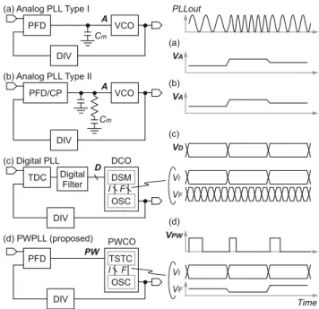
A PLL is one of the most fundamental building blocks of LSIs. Particularly, small layout area and low jitter opera- tion are strongly required for the PLL design. Conventional analog PLLs shown in Figs. 1(a) and (b) control the oscilla- tion frequency of the VCO (Voltage Controlled Oscillator).
The PFD compares the VCO output with the reference CLK input and the charge in proportion to the phase difference is injected into the LPF, and the LPF output voltage controls the VCO frequency so as to match with the reference CLK.
The PLLs in Figs. 1(a) and (b) are called Type-I and Type-II PLL, respectively. The Type-I PLL uses large capacitorCm
to convert the PFD output into control voltage for the VCO.
The Type-II PLL also uses large capacitorCmto stabilze the feedback loop. Thus, conventional analog PLLs consume large layout area as well as their analog control of degraded voltage-domain resolution in reduced supply voltage, result- ing in large jitter.
Recently, the all digital PLL structure shown in Fig. 1(c) is becoming mainstream in the advanced CMOS process. The all digital PLL converts the PFD output pulse
Manuscript received June 13, 2011.
Manuscript revised August 24, 2011.
†The authors are with the VLSI Design and Education Center (VDEC), The University of Tokyo, Tokyo, 113-0032 Japan.
a) E-mail: [email protected] DOI: 10.1587/transele.E95.C.297
Fig. 1 Typical PLL architectures and their oscillator control signals.
width into digital bits by the TDC (Time to Digital Con- verter), and the following DF (Digital Filter) outputs the dig- ital bits to control the DCO (Digitally Controlled Oscillator) frequency. The digital PLL is free from the area-consuming capacitor Cm as well as free from the subtle analog volt- age control, so that it overcomes the drawbacks of the ana- log PLL. However, the digital PLL inherently suffers from quantization noise, resulting in large jitter. One of the causes of the quantization noise is the communication between the DF and the DCO. The number of bits from the DF output is larger than the number of bits to the oscillator input in DCO, thus the DF output is dithered using a DSM (ΔΣModulator).
The other cause of the quantization noise is the TDC whose conversion resolution is limited by a single inverter gate de- lay, and most of efforts in the digital PLL design are made to realize a finer time resolution of the TDC. These additional circuits for the quantization noise reduction in the digital PLL tend to increase the number of transistors used, which makes it difficult to reduce the chip area as well as its power consumption.
This paper proposes PWCO (Pulse Width Controlled Oscillator) whose oscillation frequency is controlled by the input pulse width, and demonstrates LPF-less pulse width controlled PLL (PWPLL) using the PWCO. The PWPLL Copyright c2012 The Institute of Electronics, Information and Communication Engineers
2.1 PWCO and Soft Thermometer Code
The feedback principle of the PWPLL is similar to the Type- I analog PLL shown in Fig. 1(a). The PFD outputs the pulse whose width is the same as the phase difference between the two inputs, reference clock and the divided feedback clock.
In the Type-I analog PLL, the PFD output pulse is low pass filtered into an analog control voltage by the capacitorCm
and controls the VCO frequency, thus the ripple on the con- trol voltage induced at every rising edge of the reference clock causes jitter.
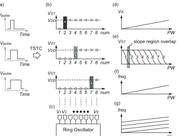
On the other hand in our PWPLL, the PWCO converts the PFD pulse width intoN bit code as shown in Figs. 2(a) and (b), where the code has many ZEROs with wider pulse width (N =8 in this figure). We call the code a soft ther- mometer code. The key point of the soft thermometer code is that the ONE/ZERO boundary has an analog voltage so as not to generate the quantization noise which the normal thermometer code inevitably has. Inside of the PWCO, the soft thermometer code is fed to the multiple terminal ring oscillator to adjust the oscillation frequency. The overall PLL block diagram is shown in Fig. 1(d), and the PLL feed- back loop locks when the PFD output pulse width, which is the same as the phase difference of the PFD inputs, corre- sponds to the appropriate soft thermometer code that gen- erates the target frequency at the ring oscillator where the divided clock has the same frequency as the input reference clock.
The relation between the PFD output pulse width PW and the oscillator control voltage are shown in Figs. 2(d) and (e) for the analog PLL, and the PWPLL, respectively, yet both of them have the similar pulse width vs. frequency re- lation as shown in Fig. 2(f). Since only one (or two) node
Fig. 2 Pulse width to soft thermometer code conversion.
require the large capacitorCm since the PFD output pulse width is not directly low pass filtered.
As shown in Fig. 2(e), the slope region of VS T i and VS T i+1 should overlap otherwise there exists a dead zone where the pulse width change is insensitive to the soft ther- mometer code change.
There is a scheme to use a digital control to select a “bank” in addition to the analog control voltage in or- der to increase the oscillation frequency range, as shown in Fig. 2(g), such as to switch ON/OFF the additional load on the ring oscillator together with the analog voltage control of the varactor. In this scheme, the nodes with the digital voltage and the nodes with the analog voltage are fixed and it requires sophisticated digital signal control. In contrast, our PWCO converts a PFD pulse into digital signals with the minimum use of an analog voltage where the node with the analog voltage changes in accordance with the incoming pulse width.
2.2 Schematics
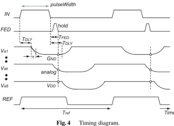
The schematics of the PWCO including TSTC (Time to Soft Thermometer code Converter) and a ring oscillator are shown in Fig. 3, and Fig. 4 shows their timing diagram. The input pulse from the PFD is delayed by DLY before entering theN stage buffer. Since each stage has a delay, the firstk stage input is ONE and the lastN−kstage input is ZERO
Fig. 3 Schematics of the time to soft thermometer code converter and the soft thermometer code controlled oscillator.
Fig. 4 Timing diagram.
at the falling edge of the input pulse, wherekdepends on the input pulse width. N =8 andk= 5 in the example of Fig. 3(b). The input of each stage is inverted by the slow in- verter denoted “s” in the inverter symbol in Fig. 3(a) in order to derive a slow fall time, and the inverter output voltageVa
is sampled and held to the output by the FED (Falling Edge Detector) pulse that is generated at the falling edge of the input pulse from the PFD, as shown in Fig. 4. In this way, the soft thermometer code output becomes that the firstk−1 stage output is ZERO, the output after thek+1 stage is ONE and the boundaryk-th stage has an analog voltage.
The converted soft thermometer code is fed to the ring oscillator whose load capacitor of each stage is controlled by the soft thermometer code input, as shown in Fig. 3. The wider pulse width from the PFD generates more ZEROs in the soft thermometer code and makes the higher oscillation frequency.
2.3 Timing Constraints
The fall time of the slow inverter is controlled by the driv- ability of the inverter and the load capacitor as shown in Fig. 3(a). The time constantτ plays an important role for generating the analog voltage for the ONE/ZERO boundary of the soft thermometer code as shown in Fig. 4.
Here, the slope region overlap betweenVS T iandVS T i+1
shown in Fig. 2(e) is realized whenτ is larger than the 1 stage delay,Tstage, and the slope region overlap gets wider as τbecomes larger. ThenVS T i,VS T i+1andVS T i+2would have slope region overlap ifτis larger than 2Tstage, but in such case, the three nodes would have analog voltage at the same time which is not desired situation for the noise tolerance.
So,
Tstage< τ <2Tstage (1)
is recommended for realizing the smooth pulse width to soft thermometer code conversion by having an appropri- ate slope region overlap ofi-th andi+1-th curve shown in Fig. 2(e).
The delay of DLY (TDLY) is set to be larger than the delay of FED (TFED) to insure thatVa of the first stage is
Fig. 5 Relations between (a) Pulse width vs. Soft thermometer code of TSTC, (b) Soft thermometer code and oscillation frequency of the ring os- cillator.
sampled and held to be ZERO before going up as shown in Fig. 4. It guarantees the monotonicity of the relation be- tween the pulse width and the soft thermometer code even when the incoming pulse width is short.
The other timing constraints is that the input pulse width should be larger than the delay of DLY and to be smaller than the N stage delay (N ·Tstage). Also the N stage delay should be smaller than the reference clock pe- riod (Perre f), to complete the soft thermometer code con- version before the next input pulse comes at the rising edge of the reference clock. These constraints are expressed as
TFED<TDLY <PW<N·Tstage<Perre f. (2)
2.4 PLL Loop Dynamics
The gain of the pulse width to soft thermometer code con- verter KT S TC[1/rad] and the gain of the soft thermometer code to the oscillator angular frequencyKRO[rad/s] are ex- pressed as
KT S TC= c2−c1
2πf0(w2−w1) (3)
KRO=2π(f2−f1)
c2−c1 (4)
wherew1, w2,c1,c2,f1,f2are shown in Fig. 5, and f0is the target frequency. Note that the unit ofwand 2πf0ware [s]
and [rad], respectively.
The transfer function of each block is as follows,
HPFD=1 (5)
HT S TC=KT S TC (6)
HRO=KRO/s (7)
Hd1=e−t1s (8)
Hd2=e−t2s (9)
HDIV =1/MDIV (10)
Hclosed= HPFDHT S TCHROHd1
1+HPFDHT S TCHROHd1HDIVHd2
= KT S TCKROe−t1s
s+KT S T CKROMe−(t1+t2)s (11)
wheret1 is the delay from PFD to the frequency change of the oscillator, and t2 is the delay of the 1/M divider cir- cuit. The closed loop transfer function of the PWPLL is expressed asHclosedof Eq. (11). When we neglect the delay t1andt2, the transfer function of our PWPLL becomes first
KPD= Δφ = 2πf0w (12)
KVCO=2πf/Vout (13)
thus
KPD·KVCO= f
f0w (14)
From Eqs. (3) and (4), KT S TC·KRO= f
f0w (15)
which is identical to Eq. (14), and both of them show the replations of PFD pulse width to output frequency conver- sion. Therefore, our PWPLL transfer function is the same as the one of a Type-I PLL with very high frequency pole LPF (equivalent with no LPF case) by replacingKPD·KVCO
withKT S TC·KRO.
2.5 Pulse Width vs. Frequency
When the input pulse enters the TSTC, the larger stage de- lay reduces the number of stages to propagate within the same pulse width period, and hence the number of ZE- ROs in the soft thermometer code is reduced, as shown in Fig. 3(a). Therefore the larger stage delay in TSTC makes KT S TCsmaller. In this case, theNstage delay can be larger as long asN·Tstage<Perre f as shown in Eq. (2).
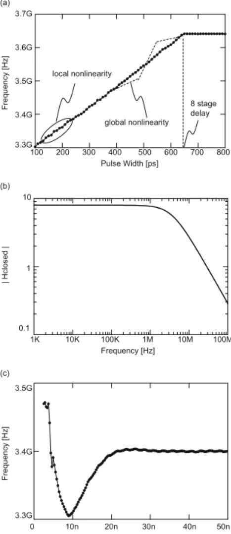
Here, the time constantτin Fig. 4 is not included in the transfer function. Theτ is used to make the slope region overlap in Fig. 2(e). However, theτmay result in local non- linearity of pulse width vs. oscillation frequency relations of PWCO as shown in Fig. 7(a), and the global nonlinearity occurs if each stage has different delay. These nonlinearity may affect the PLL loop dynamics. Here, Fig. 7(a) shows post-layout simulation results of PWCO.
The larger CL at the ring oscillator makes larger frequency change from the same soft thermometer code change, thus the largerKRO.
The maximum frequency occurs when the PWCO pulse width is the same as theNstage delays and the soft thermometer code becomes all ZERO. The minimum fre- quency occurs when the pulse width is as small asTDLY and the soft thermometer code becomes all ONE exceptVS T1
has an analog value. With this soft thermometer code, its oscillation frequency and locking range are decided by the ring oscillator withCL.
3. Chip Design and Measurement
3.1 Chip Design
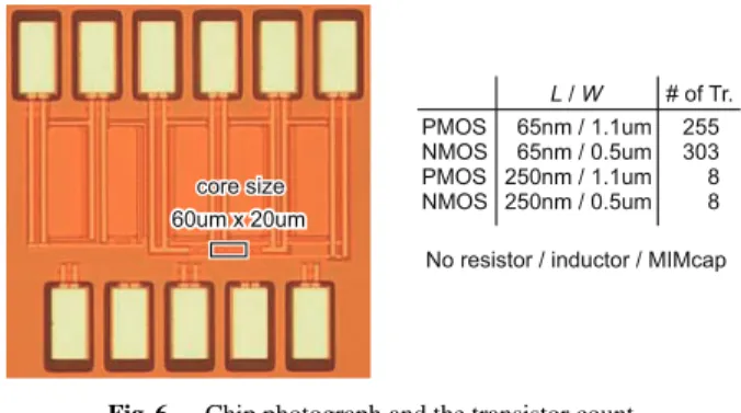
A prototype chip was designed and fabricated using 65 nm standard CMOS technology. The target frequency is
Fig. 6 Chip photograph and the transistor count.
3.125 GHz with the division ratio of M = 8 thus the ref- erence frequency is 390.625 MHz.
The number of stagesN in Fig. 3 is 8 in our design.
All the circuits except the slow inverters in Fig. 3(a) are de- signed withL=65 nm,Wp/Wn=1.1μm/0.5μm transistors in- cludingCb andCLin Figs. 3(a) and (b) consisting of 4 and 1 parallel NMOS gate capacitors, respectively. The slow inverters are designed to be L=250 nm with the same tran- sistor width. The total transistor count is 574 (NMOS 311 and PMOS 263). No resistor/inductor/MIM cap is used. The core size is as small as 1200μm2(60μm×20μm) as shown in Fig. 6.
Note thatCbin TSTC is small enough to be realized by only 4 parallel MOS gate capacitors since the time constant τis not so low as the time constant of the LPF in an analog PLL. It is also shown thatCbis not included in the transfer function in Eqs. (1)–(11). The role ofCmthat converts the input pulse width into the oscillator control code, which is an analog voltage for VCO on an analog PLL, is realized in the time to soft thermometer code conversion of TSTC using only tiny capacitors.
Figure 7 shows (a) the input pulse width vs. frequency (KT S TC·KRO) of PWCO, (b) PWPLL transfer function ex- pressed in Eq. (11) witht1=1 ns andt2=0.3 ns, (c) the tran- sient response of the output frequency. Figures 7(a) and (c) are the HSPICE post layout simulation results, and the parameters used in Fig. 7(b) are also extracted from the HSPICE post layout simulation. The bandwidth fBW is around 5 MHz from Fig. 7(b), and the locking time could be 1/(2πfBW)=32 ns, which is not so far from the transient response of Fig. 7(c).
3.2 Measurement
The measurement was conducted using on-chip direct prob- ing, as shown in Fig. 8. We used Agilent Technology Signal Generator N5181A to generate 390.625 MHz clock which is divided into two paths by a power splitter, one of which is used for the reference clock of the PLL and the other is used for the trigger of the sampling oscilloscope HP54750A in or- der to measure the 3.125 GHz (390.625 MHz×8) PLL out- put. The rms jitter from the PLL was measured to be 1.73 ps as shown in Fig. 8(b), under a 1.2 V supply with 2.81 mW power consumption. The locking range is from 2.880 GHz
Fig. 7 Post-layout simulation results of (a) Input pulse width vs. fre- quency of PWCO, (b) Transfer function of PWPLL and (c) Transient re- sponse of the output frequency.
to 3.184 GHz under a 1.2 V supply and the rms jitter is al- most constant along the locking range.
4. Discussion
4.1 Jitter Value
The measured PLL jitter was 1.73 ps, however, the sig- nal generator and the oscilloscope themselves have inter- nal jitter thus the intrinsic PLL jitter should be smaller than 1.73 ps. The signal generator is specified to have σS G ∼0.5 ps rms jitter and the oscilloscope is specified to have 2 ps rms jitter at maximum. We measured the jitter from the signal generator with the oscilloscope by splitting the signal generator output, one of which is connected to the oscilloscope signal input while the other is connected to the oscilloscope trigger, and it measuredσS G+OS C =1.46 ps as shown in Fig. 9(a). Thus the oscilloscope internal jitter is calculated to be σOS C = 1.37 ps fromσ2S G +σ2OS C = σ2S G+OS C. From the measurement results of the PLL output jitterσPLL+OS C =1.73 ps, the PLL jitter is calculated to be
Fig. 8 (a) Measurement setup, (b) Measured PLL jitter.
Fig. 9 (a) Measured jitter of the signal generator and the oscilloscope, (b) Measured PLL output spectrum.
σPLL=1.06 ps fromσ2PLL+σ2OS C=σ2PLL+OS C. In addition, since the PLL jitter includes jitter transfer from the reference clock, the intrinsic PLL jitter, which could be measured us- ing a clean reference clock with a precise oscilloscope, is estimated to be∼1 ps.
4.2 Reference Spurious
The measured PLL output spectrum is shown in Fig. 9(b).
It shows that the reference spurious noise is 38 dBc smaller than the peak power. The PFD works at every reference CLK and the SW in Fig. 3(a) switches ON and OFF, thus the ring oscillator frequency is fluctuated by the injected charge from the SW at every reference CLK. It is the cause of the reference spurious.
4.3 Comparison
The performance summary and comparison with small area and low jitter PLLs are listed in Table 1. Here the normal- ized area means the area divided by the square of the gate length and by 106: 0.0012 mm2/(65 nm)2/106 =0.29 in our case. It shows that our pulse width controlled PLL achieves small area as well as low jitter.
5. Conclusions
We have demonstrated a PWPLL without using an LPF. A PWCO accepts the PFD output where its pulse width con- trols the oscillation frequency. In the PWCO, the input pulse width is converted into soft thermometer code through a TSTC and the code controls the ring oscillator frequency.
By using this scheme, our PWPLL realizes LPF-less as well as quantization noise free operation. The prototype chip achieves 60μm×20μm layout area using 65 nm CMOS technology along with 1.73 ps rms jitter while consuming 2.81 mW under a 1.2 V supply with 3.125 GHz output fre- quency.
Acknowledgement
The VLSI chip in this study has been fabricated in the chip fabrication program of VLSI Design and Education Cen- ter (VDEC), the University of Tokyo in collaboration with STARC, e-Shuttle, Inc., and Fujitsu Ltd.
References
[1] R.B. Staszewski, K. Muhammad, D. Leipold, C.-M. Hung, Y.-C. Ho, J.L. Wallberg, C. Fernando, K.M.R. Staszewski, T. Jung, J. Koh, S.
John, I.Y. Deng, V. Sarda, O. Moreira-Tamayo, V. Mayega, R. Katz, O. Friedman, O.E. Eliezer, E. de-Obaldia, and P.T. Balsara, “All digi- tal TX frequency synthesizer and descrete-time receiver for bluetooth
G. Koo, J.H. Kim, J.H. Seo, M.L. Ko, and J.W. Kim, “A 1.2 mW 0.02 mm2 2 GHz current-controlled PLL based on a self-biased voltage-to-current converter,” ISSCC Dig. Tech. Papers, pp.310–311, Feb. 2007.
[4] K. Kim, D.M. Dreps, F.D. Ferralolo, P.W. Coteus, S. Kim, S.V. Rylov, and D.J. Friedman, “A 5.4 mW 0.0035 mm20.48 ps rms-Jitter 0.8-to- 5 GHz Non-PLL/DLL all-digital phase generator/rotator in 45 nm SOI CMOS,” ISSCC Dig. Tech. Papers, pp.98–99, Feb. 2009.
[5] X. Gao, E.A.M. Klumperink, G. Socci, M. Bohsali, and B. Nauta,
“Spur-reduction technique for PLLs using sub-sampling phase detec- tion,” ISSCC Dig. Tech. Papers, pp.474–475, Feb. 2010.
Toru Nakura was born in Fukuoka, Japan in 1972. He received the B.S., and M.S. degree in electronic engineering from The University of Tokyo, Tokyo, Japan, in 1995 and 1997 respec- tively. Then he worked as a high-speed com- munication circuit designer using SOI devices for two years, and worked as a EDA tool devel- oper for three years. He joined the University of Tokyo again as a Ph.D. student in 2002, and received the degree in 2005. After two years in- dustrial working period, he is now an associate professor at VLSI Design and Education Center (VDEC), The Univer- sity of Tokyo. His current interest includes signal integrity, reliability and digitally-assist analog circuits.
Kunihiro Asada was born in Fukui, Japan, on June 16, 1952. He received the B.S., M.S., and Ph.D. in electronic engineering from the University of Tokyo in 1975, 1977, and 1980, respectively. In 1980 he joined the Faculty of Engineering, the University of Tokyo, and be- came a lecturer, an associate professor and a professor in 1981, 1985 and 1995, respectively.
From 1985 to 1986 he stayed in Edinburgh the University as a visiting scholar supported by the British Council. From 1990 to 1992 he served as the first Editor of English version of IEICE (Institute of Electronics, Infor- mation and Communication Engineers of Japan) Transactions on Electron- ics. In 1996, he established VDEC (VLSI Design and Education Center) with his colleagues in the University of Tokyo. It is a center supported by the Government to promote education and research of VLSI design in all the universities and colleges in Japan. He is currently in charge of the head of VDEC. His research interests are design and evaluation of integrated systems and component devices. He has published more than 400 techni- cal papers in journals and conference proceedings. He has received Best Paper Awards from IEEJ (Institute of Electrical Engineers of Japan), and ICMTS1998/IEEE and so on. He is a member of the Institute of Electrical and Electronics Engineers (IEEE), and the Institute of Electrical Engineers of Japan (IEEJ).