Tile/Line Dual Access Cache Memory based on Hierarchical Z-order Tiling Data Layout
by
BaoKang Wang
(415DB53)
The Division of Systems Engineering,
Graduate School of Engineering, Mie University.
Tsu, Mie March, 2018
APPROVED BY:
Dr. Toshio Kondo (Chair of Advisory Committee) Dr. Tetsushi Wakabayashi
Dr. Yoshikatsu Ohta
ABSTRACT
The increasing disparity between the data access speed of cache and process- ing speeds of processors has recently caused a major bottleneck in achieving high- performance 2-dimensional (2-D) data processing, such as that in image processing and scientific computing. However, multi-core and single instruction multiple data (SIMD) extensions are current technologies that can effectively improve the process- ing speeds of processors. Even though 2-D data are generally arranged in row-major layout (C language) or column-major layout (Fortran language) in memory, single- directional layouts have poor locality for 2-D data access because vertically adjacent data are stored far apart. As a result, the translation lookaside buffer (TLB) misses frequently occur and the excessive data transfer problem cannot be avoided by using conventional caches. Therefore, ineffective non-major-directional data access to cache memory has become a bottleneck for efficient 2-D data processing by utilizing extended SIMD instructions.
This thesis proposes a cache memory with both tile (column and row directions) and line (row direction) accessibility for efficient 2-D data processing to solve this problem.
The proposed cache is based on a 4-level Z-order tiling data layout and a multi-bank memory array structure that supports skewed array storage schemes. 2-D data access to the proposed cache memory is enabled via a hardware-based multi-mode address translation unit that eliminates the overhead of software-based address calculation and transforms the conventional raster layout into the 4-level Z-order tiling data layout.
The proposed layout maximizes utilization of the 2-D reference locality, minimizes the TLB misses, and reduces the amount of excessive data transfer by dividing the data into hierarchical 3-level tiles (the 1st-level is a 2048 × 2048 byte-sized large tile, the 2nd-level is a 64 × 64 byte-sized medium tile and the 3rd-level is an 8 × 8 byte-sized tile), each of which is arranged in raster scan order at the same level.
In addition, the author has added a dual 1-D/2-D data access mode to the proposed cache. The proposed cache can appropriately switch a 2-D access mode for the proposed tile and line access to a 1-D data access mode for conventional raster line access.
Therefore, the proposed cache can be used for both 1-D and 2-D data processing. The author proposes a method of reducing tag memory to replace multiple tiles with an aligned tile set (RATS) in the cache to reduce the hardware overhead of the proposed cache. The RATS method greatly reduces the entire hardware scale and simplifies the cache architecture, even though it provides almost the same cache performance.
The author evaluated the proposed cache in two ways: First, to verify the feasibility
of the proposed cache, a large-scale integration (LSI) layout of a SIMD-based general
purpose-oriented datapath that embedded the proposed cache was designed in a 2.5 × 5
mm
2area using 0.18 µ m complementary metal oxide semiconductor (CMOS) technol-
ogy. The read latency was limited to 3 clock cycles under a 3.9 ns clock period (250
MHz), which was the same as that for the conventional cache memory of an Intel or
advanced reduced instruction set computer (RISC) machine (ARM) high-performance
processor. The entire hardware overhead of the proposed RATS-cache was reduced to only 7% of that required for a conventional cache by using the RATS method.
In addition, the author evaluated the performance of the proposed cache for matrix multiplication (MM) and LU decomposition (LUD) in terms of the number of L1, L2 cache and TLB misses and the execution time (cycles). The results from simulation for the proposed cache indicated a considerable reduction in L1 and L2 cache conflict misses compared with a conventional cache in power-of-two matrix size due to the column-directional address stride being sufficiently smaller than the page size. In addition, the proposed cache significantly improved the TLB performance compared to a conventional cache with all matrix sizes. Therefore, the proposed cache provided efficient column-directional parallel access that was the same as row directional parallel access so that it enabled efficient SIMD operation that required no transposition in MM. The proposed cache could provide almost the same performance as LUD for the column-major based LUD program as that for the row-major based LUD program.
These results indicated that the proposed cache did not restrict our freedom in selecting either row- or column-major order coding. In addition, the results from simulation also revealed that the RATS cache and the Non-RATS cache (the proposed cache did not adopt the RATS method) provided almost the same performance, which was not inferior to that of the conventional cache.
Finally, the number of parallel load instructions required for parallel column- and
row-directional access was reduced to about one fourth of that required for conventional
raster line access for MM. Since the performance of the proposed cache was also affected
by the performance of L1 and L2 caches, the execution time for parallel load instruction
was about one third of that required for conventional load instruction. The proposed
cache with tile/line accessibility further improved the performance of 2-D applications
by using SIMD instructions.
Contents
1 Introduction 1
1.1 Background and related work . . . . 1
1.2 Approach and main contributions of this thesis . . . . 3
1.3 Thesis Organization . . . . 6
2 Current insufficient utilization of 2-D spatial reference locality 7 2.1 Conventional raster layout . . . . 7
2.1.1 Layout features . . . . 7
2.1.2 Difficulty of the 2-D locality utilization . . . . 8
2.1.2.1 Problems with TLB misses for large-sized 2-D data access 9 2.1.2.2 Excessive data transfer problem . . . . 10
2.1.2.3 Parallel data access capability in the major direction . 11 2.2 Conventional methods of improvement . . . . 12
2.2.1 Usage of transposition . . . . 12
2.2.2 Cache tiling . . . . 14
2.2.2.1 Software-based cache tiling method . . . . 15
2.2.2.2 Hardware-based cache tiling method . . . . 16
2.2.2.3 Problem of the cache tiling method . . . . 18
2.2.3 Hardware prefetching . . . . 19
3 Current SIMD instruction set extensions 21 3.1 SIMD parallel processing . . . . 21
3.2 Gather/scatter operations . . . . 23
3.2.1 Non-contiguous memory access by gather and scatter operations 23 3.3 Efficient transposition . . . . 24
3.3.1 Transposition routine with Intel AVX2 . . . . 24
3.4 Non-major-directional operation in the Intel library . . . . 26
4 Skewed storage scheme 28
4.1 Parallel row- and column-directional access by using skewed storage scheme 28
4.1.1 Skewed storage scheme . . . . 28
4.1.2 Parallel non-major-directional tile access by using skewed storage
scheme . . . . 30
5 Hierarchical tiling data layout 34 5.1 Effectiveness of hierarchical tiling data layout . . . . 34
5.1.1 Block data layout . . . . 34
5.1.2 Z-Morton layout . . . . 35
5.1.3 Morton hybrid layout . . . . 38
5.2 Problem of the hierarchical tiling data layout . . . . 40
6 Proposed cache memory with tile and line accessibility 42 6.1 Proposed Multi-level Z-order tiling data layout . . . . 42
6.1.1 4-level Z-order tiling data layout . . . . 42
6.1.2 Cache-based hybrid Z-ordering layout . . . . 44
6.1.2.1 Utilization of hardware prefetching . . . . 45
6.1.2.2 Strassen algorithm for MM . . . . 48
6.2 The proposed cache architecture . . . . 49
6.2.1 Parallel tile and line accessibility . . . . 50
6.2.2 Improvement of data transfer speed . . . . 51
6.2.3 Improvement of degree of coding flexibility for 2-D program . . 52
6.2.4 Load instructions reduction by using SIMD extensions . . . . . 52
6.3 Parallel tile and line access mechanism . . . . 52
6.4 Hardware-based address bit-order interchange unit for raster scan order to the 4-level Z-order tiling space . . . . 55
6.5 Tag memory reduction method . . . . 58
6.6 Unaligned tile access in the column direction . . . . 60
6.7 Dual data access mode for 1-D/2-D data access . . . . 61
7 Hardware scale optimization of the proposed cache 62 7.1 RATS-tag memory reduction method . . . . 62
7.1.1 RATS-T access mode . . . . 64
7.1.2 RATS-S access mode . . . . 64
7.2 The proposed RATS-cache architecture . . . . 65
8 Evaluation 66 8.1 Hardware scale evaluation . . . . 66
8.1.1 Implementation . . . . 66
8.1.2 Hardware scale overhead and speed performance evaluation . . . 66
8.1.3 Critical path for loading . . . . 68
8.2 Performance evaluation . . . . 70
8.2.1 Execution environment . . . . 71
8.2.2 RATS-T access evaluation . . . . 73
8.2.2.1 Performance of multi-level cache and TLB . . . . 73
8.2.2.2 Execution time evaluation . . . . 76
8.2.3 RATS-S access evaluation . . . . 79
8.2.3.1 Performance of multi-level cache and TLB . . . . 79
8.2.3.2 Execution time evaluation . . . . 82
8.2.4 Parallel tile/line access evaluation . . . . 83
8.2.4.1 Evaluation of reduction to load instructions . . . . 83
8.2.4.2 Execution time evaluation . . . . 84
9 Conclusion 87 A Appendix 90 A.1 Number of cycles required for data loadings . . . . 90
References 93
List of Figures
2.1 Raster layout: row-major order with 8 × 8 sized matrix. . . . 8
2.2 Raster layout: column-major order with 8 × 8 sized matrix. . . . 8
2.3 Excessive data transfer in raster data access. . . . 11
2.4 Mapping a 2-D matrix to row-major layout. . . . 12
2.5 Transpose a row-major order based 8 × 8 matrix to a column-major order based 8 × 8 matrix. . . . 13
2.6 Excessive data transfer in raster data access. . . . 14
2.7 Tiled and untiled MM. . . . 15
2.8 Software-based tiling. . . . 16
2.9 Hardware-based tiling. . . . 17
3.10 SIMD addition: C = A + B. . . . 22
3.11 Gather operation: VGATHERDPS instruction. . . . . 24
3.12 Elements permutation in YMM register: VPERM instruction. . . . 25
3.13 4 × 4 transposition processing. . . . 25
4.14 4-bank structured memory. . . . 29
4.15 4-bank structured memory that supports skewed storage scheme. . . . . 29
4.16 Block-offset mapping. . . . 30
4.17 8 × 4 byte-sized tile access by using skewed storage scheme. . . . 32
4.18 4 × 8 byte-sized tile access by using skewed storage scheme. . . . 32
4.19 Block-offset mapping for a large-sized 2-D data access. . . . 33
5.20 Block data layout, using 4 × 4 tile. . . . 35
5.21 Z-Morton layout. . . . 36
5.22 Z-Morton layout: 16 × 16 matrix. . . . 39
5.23 Morton hybrid layout: 16 × 16 matrix. . . . 40
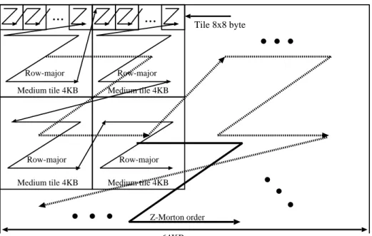
6.24 4-level Z-order tiling layout. . . . 43
6.25 Medium tile and tile store data in raster scan order. . . . 43
6.26 Cache-based hybrid Z-ordering layout (Medium tile and tile store data in raster scan order). . . . 44
6.27 Strassen algorithm performs a single level recursion 2 × 2 tile. . . . 48
6.28 Block diagram of the proposed cache memory. . . . 50
6.29 Tile data access. . . . 51
6.30 Conventional storage scheme. . . . 53
6.31 Parallel tile and line access scheme (line access). . . . 54
6.32 Parallel tile and line access scheme (tile access). . . . 54
6.33 Various sizes of 2-D data allocation in the 4-level Z-order tiling layout. 56 6.34 Memory allocation for 4-level Z-order tiling space. . . . 57
6.35 The address bit interchange. . . . 57
6.36 Address translation circuit. . . . 58
6.37 Each tag is added to each constituent subline of a skewed array com- posing an aligned tile. . . . 59
6.38 Each tag is added to each aligned tile. . . . 59
6.39 Unaligned tile access scheme. . . . 60
6.40 Proposed cache for both 1-D and 2-D data processing. . . . . 61
7.41 Aligned tile set in each medium tile. . . . 63
7.42 Two-bank tag memory structure. . . . 64
7.43 Block diagram of the proposed RATS-cache memory. . . . 65
8.44 Chip layout. . . . 68
8.45 Critical path for loading of the proposed 2-way/8-way set associative cache. . . . 70
8.46 RATS-T access, N × N MM: Number of DL1 cache misses. . . . 73
8.47 RATS-T access, N × N LUD: Number of DL1 cache misses. . . . 75
8.48 RATS-T access, N × N MM: Number of UL2 cache misses. . . . 76
8.49 RATS-T access, N × N LUD: Number of UL2 cache misses. . . . 76
8.50 RATS-T access, N × N MM: Number of TLB misses. . . . 77
8.51 RATS-T access, N×N LUD: Number of TLB misses. . . . 77
8.52 RATS-T access, overall speedup for MM. . . . 78
8.53 RATS-T access, overall speedup for LUD. . . . 78
8.54 RATS-S access, N × N MM: Number of DL1 cache misses. . . . 79
8.55 RATS-S access, N × N LUD: Number of DL1 cache misses. . . . 79
8.56 RATS-S access, N × N MM: Number of UL2 cache misses. . . . 80
8.57 RATS-S access, N × N LUD: Number of UL2 cache misses. . . . 80
8.58 RATS-S access, N × N MM: Number of TLB misses. . . . 81
8.59 RATS-S access, N × N LUD: Number of TLB misses. . . . 81
8.60 RATS-S access, overall speedup for MM. . . . 82
8.61 RATS-S access, overall speedup for LUD. . . . 82
8.62 Number of load instruction reduction. . . . 84
1.63 Evaluation results in the HorseRace sequence. . . . 91
1.64 Evaluation results in the Bronze with credits sequence. . . . 91
List of Tables
2.1 Throughout count breakdown of DCT in videolan x264. . . . 14
4.2 Access count reduction rate. . . . 31
5.3 Theoretical cache and TLB hit rate for row-directional access of a large- sized 2-D array of double-precision floating-point operations. We do not consider the additional conflict misses due to 2-D data locality. . . . 37
5.4 Theoretical cache and TLB hit rate for column-directional access of a large-sized 2-D array of double-precision floating-point operations. We do not consider the additional conflict misses due to 2-D data locality. . 37
6.5 Theoretical cache and TLB hit rate for MM with double-precision floating- point operations. The author does not consider the additional conflict misses due to 2-D data locality. . . . 47
6.6 Theoretical cache and TLB hit rate for MM with single-precision floating- point operations. The author does not consider the additional conflict misses due to 2-D data locality. . . . 47
6.7 Strassen algorithm. . . . 48
8.8 Chip specification. . . . 67
8.9 Cache speed. . . . . 67
8.10 Hardware scale for the 2-way set associative cache (Number of NAND gate equivalents). . . . 69
8.11 Hardware scale for the 8-way set associative cache (Number of NAND gate equivalents). . . . 69
8.12 Processor and memory hierarchy configuration. . . . 72
8.13 DL1 Cache miss rate for MM. . . . 73
8.14 DL1 Cache miss rate for LUD. . . . 74
8.15 The number of DL1 and UL2 cache misses for parallel tile and line access. 85 8.16 Execution time evaluation. . . . 86
1.17 Condition of the simulation. . . . 90
1 Introduction
1.1 Background and related work
Although computer performance has been considerably improving year by year, the demand for efficient 2-D data processing, such as that in numerical calculations, image processing, object recognition, and video coding, continues to increase. Improvements to processor and memory access speeds are important keys to improve the performance of 2-D data processing. Multi-core and single instruction multiple data (SIMD) exten- sions are current technologies that can effectively improve processing speeds [1] [2].
However, sufficiently efficient data access for parallel processing has not yet been ob- tained because conventional cache memory, which is based on either row- or column- major data layouts (raster or single-directional layouts), does not enable efficient opera- tions to spatially reference 2-D data, such as those used in image processing or scientific computing. For example, conflict misses and translation lookaside buffer (TLB) misses have frequently occurred in large-scale matrix multiplication (MM) because the cache memory does not contain all the data needed for the program’s execution or exploit 2-D data locality in the column direction. In addition, the raster layout is inefficient to access two-dimensionally localized block data in image processing, and the excessive data transfer problem cannot be avoided [3] [4].
A software-based, single-levels tiling technique (also known as blocking) has been
used to effectively improve 2-D data access capability to solve these problems. This
technique allows the cache to exploit temporal locality; therefore, this tiling technique
can reduce the cache capacity miss rate. However, 2-D data processing by using SIMD
operations is restricted because there is no availability of a column-directional parallel
access function so that performance degradation cannot be avoided if it does not use
manually or ingeniously optimized routines such as the OpenBLAS or the Intel math
kernel library (MKL). Also, the tiling technique does not effectively reduce the number
of TLB misses and the amount of excessive data transfer for two-dimensionally localized
block data access. User-transparent tile-based addressing, on the other hand, which
requires no address translation in the user software, relies on the compiler to restructure
the loop code, which causes additional overhead in the execution time because the cost
of tiling address computation cannot be avoided [5] [6] [7].
Hierarchical tile based addressing on the Z-Morton layout [8] is a more effective technique than conventional single-level tiling in terms of reducing column-directional conflict misses and TLB misses in the processing of power-of-two sized matrices. The Z-Morton layout, which is, a potential compromise between row- and column-major layouts [9] [10] can minimize conflict misses and TLB misses in both row and column directions and utilize the spatial reference locality, regardless of the data array size.
However, address calculation for the Morton layout is considerably more complex than that for the row- or column- major layouts, which causes significant processing over- head. As such, Morton address calculation imposes a software-overhead cost to exploit the 2-D spatial reference locality benefits of the Z-Morton layout.
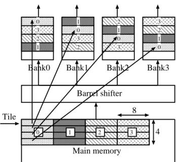
Wittenbrink and Somani [11] proposed a hardware approach with three important advantages over the software approach: 1) the image storing and transfer mechanisms, such as direct memory access (DMA) or I/O devices, are independent of the tiling scheme, 2) a small tile can be used to process images of an arbitrary size, and most importantly, 3) the address translation is transparent to the user software. Although this approach is highly effective in reducing the execution time, two problems remain to be solved: 1) each width of the 2-D processing area requires a different address bit-order interchange and 2) the approach cannot support simultaneous parallel small tile access.
Although other studies [12] [13] [14] [15] [16] have used the Morton layout to exploit 2-D data locality and reduce conflict misses and TLB misses, these approaches have increased the cycle time or access latency due to the versatility of Morton-index trans- lations. In contrast, [17] proposed a hardware-based bit-permuting unit to translate the raster scan order address to a Z-Morton address that indicated that the hardware- based method reduced the overhead of Z-Morton address calculation (total number of instructions) by about 40% compared with that of the software-based method on a superscalar processor [18]. However, the main focus of this study was not to ob- tain column-directional parallel access capability but to facilitate the reduction of the software overhead for Z-Morton address calculation.
The author proposes a new cache memory architecture for one-dimensional and
two-dimensional (1-D/2-D) data processing to eliminate these problems and combine it with a SIMD-based general purpose-oriented datapath [19] [20]. Our method provides more advanced features of a cache line-sized tile or line accessibility than the previous hardware and software cache tiling techniques and a user-transparent hybrid Z-order tile-based address implemented without additional latency.
1.2 Approach and main contributions of this thesis
The 13 most outstanding specific contributions of this thesis are highlighted below:
1. The author proposes a new 8-way set associative cache (32 Kbytes with a 64- byte cache line) with an 8×8 byte-sized tile and 64-byte-sized line accessibility.
Its parallel aligned/unaligned tile and line access corresponding to parallel data access in the column and row directions can improve throughput with a low latency overhead.
2. The tile access corresponding to column-directional parallel data access can elim- inate the transposition required in matrix calculation, orthogonal transform such as fourier transform or discrete cosine transform (DCT) and image feature detec- tion, and it can provide efficient 2-D unit block access for image processing and video coding, even though its utilization may require significant modifications to the program code.
3. The author proposes a method of reducing tag memory that replaces multiple tiles with an aligned tile set (RATS) in the cache to reduce the hardware overhead of the proposed cache. The RATS method considerably reduces the entire hardware scale of the proposed cache and simplifies the cache architecture without affecting cache performance.
4. The proposed cache can minimize TLB misses in both row and column direction
in 2-D processing. As a result, it can minimize the optimization efforts of an
original tiling code in which it is difficult to utilize manually coded libraries such as
OpenBLAS or Intel MKL. In other words, the proposed cache provides a column-
directional parallel access function and allows either row-major based or column-
major based 2-D program code so that it increases the degree of freedom of coding.
Therefore, the programmer’s burden of coding to improve processing efficiency can be reduced by using our proposed cache.
5. The column-directional address stride becomes sufficiently smaller than the 4 Kbytes page size (virtual memory page size) in the 4-level Z-order tiling layout. This small stride minimizes the conflict misses and TLB misses in the column-directional ad- jacent or contiguous access. As a result, the proposed cache can provide efficient column-directional access as well as row directional access with a minimal hardware increase so that it enables efficient SIMD operations that require no transposition in matrix computation.
6. The proposed cache scheme can be freely configured from a direct-mapped cache to an n-way set associative cache. To the best of my knowledge, the author is the first to design a high-performance on-chip n-way set associative cache memory with tile/line accessibility for 2-D data processing and combine the proposed cache with a general purpose-oriented datapath that supports SIMD extensions. The author also evaluates three main specifications to demonstrate the feasibility of the proposed cache: read and write latency, clock period, and hardware scale.
7. The author adds a dual data access mode to the proposed cache memory to support the conventional raster line access for 1-D data processing. The proposed cache can appropriately switch a 2-D data access mode for the proposed tile and line access to a 1-D data access mode for the conventional raster line access.
8. The author proposes a new data layout called the 4-level Z-order tiling layout based on the conventional Z-Morton layout to maximize the exploitation of 2-D reference locality, reduce cache misses and TLB misses and reduce the amount of excessive data transfer. The proposed 4-level Z-order tiling layout divides data into hierarchical 3-level tiles (1st-level large tiles, 2nd-level medium tiles and 3rd-level tiles), each of which is arranged in raster scan order at the same level.
9. The author proposes a new data layout called the Cache-based hybrid Z-ordering
layout based on the 4-level Z-order tiling layout and the conventional Z-Morton
layout to efficient exploit hardware prefetching technique. The proposed layout
can exploit constant-stride prefetching in both major-directional and non-major directional access. In addition, combining the Strassen algorithm with the proposed layout can improve MM performance for any matrix size.
10. The address bit-order interchanger in the proposed cache is performed by hardware and is transparent to the processor. This address bit-order interchange that cor- responds to a 64 Kbytes-wide area eliminates the address calculation overhead of Morton-index conversion for 2-D data access and allows the 4-level Z-order (based on the Z-Morton layout) curve tiling layout to be accessed as a conventional raster layout.
11. The author evaluates the performance of the proposed cache for MM and LUD in terms of the number of L1, L2 cache and TLB misses and the execution time (cycles). The results obtained from evaluation revealed that the RATS cache and the Non-RATS cache provide almost the same performance in matrix computation, which is not inferior to that of the conventional cache.
12. The author evaluates the hardware scale overhead of the RATS cache. Compared with the conventional cache, the entire hardware scale overhead of the RATS cache is reduced to only 5% and 7% for an 8-way set associative cache with a 32-byte cache line for the former and a 64-byte cache line for the latter. The RATS cache provides almost the same performance as that of the Non-RATS cache although it require only a minimum addition of hardware for both tile and line accessibility.
13. The author modifies the SimpleScalar simulator and evaluates the performance of load instruction reduction (SIMD processing) for parallel tile and line access. The results from evaluation indicated that the number of load instructions for SIMD processing is reduced to about one fourth of that required for non-SIMD processing.
The execution cycles for SIMD processing is reduced to about one third of those required for non-SIMD processing due to the effect of L1 and L2 caches misses.
The proposed cache with tile/line accessibility further improves the performance of
2-D applications by using SIMD instructions.
1.3 Thesis Organization
The remainder of this paper is organized as follows. Background information related
to the thesis is described in Section 2. This section introduces the conventional raster
layout and cache tiling method. Current SIMD instruction set extensions are described
in Section 3. This section introduces the current SIMD architecture, the Intel MK-
L/IPP library and non-contiguous memory access operation by using gather/scatter
instructions. Skewed storage scheme is described in Section 4. This section introduces
parallel data access in the row and column direction can be realized by using multi-bank
memory structure that supports skewed storage scheme. Section 5 compares various
hierarchical tiling data layouts such as the single-level tiling layout, multi-level Z-order
tiling layout, Z-Morton layout and Morton hybrid layout. The proposed 4-level Z-order
tiling data layout, the proposed cache architecture design, address translation unit and
parallel tile/line access scheme are presented in Section 6. The RATS tag memory
reduction method is presented in Section 7. The design result of the proposed cache
and the performance evaluation results are presented in Section 8. Finally, the author
provides a discussion and conclusion in Section 9.
2 Current insufficient utilization of 2-D spatial ref- erence locality
2.1 Conventional raster layout
Matrices in most language implementations are usually stored in contiguous memory locations using either row-major or column-major raster layout. Figures 2.1 and 2.2 outline the configurations for row-major and column-major layouts. As shown in Figure 2.1, the row-major layout stores the first row of a 1-D matrix in contiguous memory, and then the second, etc. As shown in Figure 2.2, the column-major layout stores the first column of a 1-D matrix in contiguous memory, and then the second, etc. Therefore, consecutive elements of the rows of the matrix are stored in contiguous memory in the row-major layout and consecutive elements of the columns of the matrix are stored in contiguous memory in column-major layout. The raster layout is also called 1-D contiguous order layout. The row-major layout is by far the most commonly used today as it has been adopted in C language.
2.1.1 Layout features
There are three main advantages of the raster layout. (1) It is easy to generate the address of each element since the address linearly increases in the major, i.e, either in the row or column direction. (2) If the accessed data are stored in the same page, they do not occur TLB misses. If the accessed data are stored in the same cache line, they can be loaded onto the processor in one cycle. Therefore, all the contiguous elements linearly arranged in the raster layout can be fetched very quickly in the major direction. Parallel access by using the cache line in the major direction can be achieved.
However, the raster layout provides poor access capability for 2-D arrays unless the data are accessed in the major direction (for a row-major layout, the row direction is the major direction and the column direction is a non-major direction). (3) This is efficient for 1-D data processing because the range of the same tag values maximizes in the major direction.
However, efficient access is only provided in the major direction because the ele-
ments for parallel access must be stored in almost the same cache line or the same
1 2 3 4
0 5 6 7
9 10 11 12
8 13 14 15
17 18 19 20
16 21 22 23
25 26 27 28
24 29 30 31
33 34 35 36
32 37 38 39
41 42 43 44
40 45 46 47
49 50 51 52
48 53 54 55
57 58 59 60
56 61 62 63
Figure 2.1: Raster layout: row-major order with 8 × 8 sized matrix.
8 16 24 32
0 40 48 56
9 17 25 33
1 41 49 57
10 18 26 34
2 42 50 58
11 19 27 35
3 43 51 59
12 20 28 36
4 44 52 60
13 21 29 37
5 45 53 61
14 22 30 38
6 46 54 62
15 23 31 39
7 47 55 63
Figure 2.2: Raster layout: column-major order with 8 × 8 sized matrix.
page. As a result, the raster layout has poor accessibility in the non-major direction for large-sized 2-D data. Non-major-directional contiguous access causes frequent TLB misses if the stride length is greater than the page size of virtual memory so that the non-major directional contiguous access exceeds the TLB size. Consequently, the raster layout is inefficient for 2-D data access.
2.1.2 Difficulty of the 2-D locality utilization
This raster layout does not lead to good access efficiency for 2-D data without a skillful
or tricky processing algorithm. This is because the raster layout imposes stride ad-
dressing on non-major directional contiguous elements so that it makes parallel data
access difficult in the non-major direction and it can only provide efficient access ca- pability in the major direction. In addition, the raster layout causes problem with frequent TLB misses in large-sized 2-D data access due to the small TLB sizes such as those with 64 entries.
2.1.2.1 Problems with TLB misses for large-sized 2-D data access
The processor generates logical addresses that just become virtual addresses. In addition, physical addresses are used to access memory. TLB is a cache of memory that stores recent translations of virtual to physical addresses for faster retrieval. Therefore, TLB only stores the most recently accessed page table entries. A TLB miss occurs when it does not contain the tag entry for translating a virtual address to a physical address.
If there is a TLB miss, the translation proceeds by looking up the page table in a process. A page fault occurs if the processor accesses data that cannot be found either in the TLB or in the main memory.
The raster layout causes frequent TLB misses for large-sized 2-D data access due to the small TLB size. The major-directional small address stride for 2-D data access is mostly not over the page size whereas the non-major-directional large address stride (stride length is greater than page size) always exceeds the page size and it often causes TLB misses. Therefore, non-major directional access causes frequent TLB misses.
Consider large scale matrices storing elements in a row-major layout for MM. Column- directional access causes frequent TLB misses because the address of elements in each column are mapped to a different page.
Listing 1: The basic MM version (ijk).
1
int main ()
2
{
3
for ( i = 0; i < 32; i ++)
4
for ( j = 0; j < 32; j ++)
5
for ( k = 0; k < 32; k ++)
6
C [ i ][ j ]+= A [ i ][ k ] * B [ k ][ j ];
7
}
Suppose that there are three matrices, A, B, and C, each of which is a 32 × 32 matrix composed of double precision elements and laid out in memory in row-major order and that their beginning is aligned to a page boundary (e.g., A[0][0] is located at the beginning of a page and B[0][0] is located on another page.). Consider the basic MM algorithm in ijk order as shown in Listing 1.
Assume the page size is 8 Kbytes and 256 Kbytes of physical addresses are covered by a 32 entry TLB. Each matrix needs 2
5× 2
5× 2
3= 8 Kbytes. The column-directional elements of matrix B accessed from the different rows are in the same page in the k loop scans, so that a TLB miss is caused in the element access. Consider the matrix size in Listing 1 is N × N where N is larger than the page size. The memory pages are accessed consecutively in the row-directional matrix A access. As a result, TLB misses caused by row-directional access are equal to N
2/P (P is the page size). In contrast, the number of the TLB misses in the column-directional matrix B access is almost equal to N since accessing a different row causes a TLB miss since each row is assigned to N different pages. Consequently, the more matrix size sharply increases, and the TLB misses increase since the row-major layout cannot exploit the 2-D reference locality in the column direction.
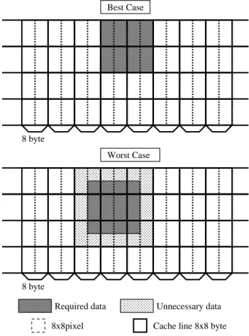
2.1.2.2 Excessive data transfer problem
The raster layout also cannot provide efficient access to the 2-D localized array
data because it only provides the data transmission function by cache line in the major
direction. For example, in block matching for motion search or image recognition, the
typical cache line size from 32 to 256 bytes is too long to load a block equal to or less
than the conventional 16 × 16 pixel block so that more than half of the accessed cache
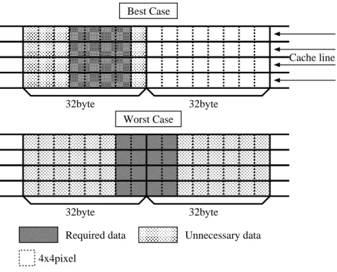
line data is unused. As shown in Figure 2.3, a 32 byte cache line contains a number of
data unnecessary for the 16 × 16 pixel macroblock access. If the required data are across
the two adjacent cache lines, 64 × 16 pixel data transmission is required nevertheless
the 48 × 16 pixel of the transmitted data may be unused. This inefficient raster data
access frequently occur in the feature detection of the motion recognition.
32byte 32byte
32byte 32byte
Required data Unnecessary data Worst Case
Best Case
4x4pixel
Cache line
Figure 2.3: Excessive data transfer in raster data access.
2.1.2.3 Parallel data access capability in the major direction
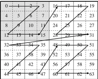
The elements of each column in row-major layout are non-contiguous in memory even though the elements of each row are contiguous in memory. Therefore, the row- major layout only provides row-directional parallel access capability.
Figure 2.4 show that an 8 × 8 matrix is stored in row-major layout. The processor
contiguously accesses the elements of the matrix in the row direction. Once the start
address of a row is obtained, the contiguously accessed elements in the row direction
can be fetched very quickly because they are almost in the same cache line or in the
same page. However, the processor cannot parallel access elements of the matrix in
the column direction since the address stride between adjacent elements in the column
direction is determined by the 2-D data width. Therefore, the accessed elements may
be stored in the same memory bank and cannot be read out in parallel even if the
cache memory is composed of a multi-bank structure. Consequently, only part of the
data can be read out in parallel.
0,1 0,2 0,3 0,4
0,0 0,5 0,6 0,7
1,1 1,2 1,3 1,4
1,0 1,5 1,6 1,7
2,1 2,2 2,3 2,4
2,0 2,5 2,6 2,7
3,1 3,2 3,3 3,4
3,0 3,5 3,6 3,7
4,1 4,2 4,3 4,4
4,0 4,5 4,6 4,7
5,1 5,2 5,3 5,4
5,0 5,5 5,6 5,7
6,1 6,2 6,3 6,4
6,0 6,5 6,6 6,7
7,1 7,2 7,3 7,4
7,0 7,5 7,6 7,7
Figure 2.4: Mapping a 2-D matrix to row-major layout.
2.2 Conventional methods of improvement
2.2.1 Usage of transposition
Since elements in the non-major direction in raster layout are stored in non-contiguous locations in memory, non-major-directional contiguous access may cause significant performance degradation. Transposition of the turning row (column) into the column (row) has been used to solve this ineffective data access problem. For example, let us consider that the matrix in Figure 2.4 stores elements in row-major layout. Transposi- tion can be used to enable the column data in Figure 2.5 to be contiguously accessed.
Transposition is required for 2-D data applications, such as matrix calculation, fast fourier transform (FFT), DCT or inverse discrete cosine transform (IDCT). Here, DCT is often used in image compression and video encoding. DCT in video encoding requires the second largest amount of operation and occupies about 10 to 20% of the total amount of encoding operations. Generally, N × N 2-D DCT consists of horizontal 1-D DCT and vertical 1-D DCT computing. The horizontal 1-D DCT processes data in the row direction while the vertical 1-D DCT processes data in the column direction.
Horizontal 1-D DCT is simply performed with high processing efficiency since it is
composed of 1-D operations in the row major layout. However, vertical 1-D DCT
suffers from the high processing load of prior transposition that is required to match
its column-directional operation to the row-major layout for efficient 1-D operation.
1,0 2,0 3,0 4,0
0,0 5,0 6,0 7,0
1,1 2,1 3,1 4,1
0,1 5,1 6,1 7,1
1,2 2,2 3,2 4,2
0,2 5,2 6,2 7,2
1,3 2,3 3,3 4,3
0,3 5,3 6,3 7,3
1,4 2,4 3,4 4,4
0,4 5,4 6,4 7,4
1,5 2,5 3,5 4,5
0,5 5,5 6,5 7,5
1,6 2,6 3,6 4,6
0,6 5,6 6,6 7,6
1,7 2,7 3,7 4,7
0,7 5,7 6,7 7,7
Figure 2.5: Transpose a row-major order based 8 × 8 matrix to a column-major order based 8 × 8 matrix.
The author has analyzed VideoLANx264, which is the most popular open source encoder software for H.264 [21], to speed-up the 2-D DCT. This VideoLANx264 ob- tains a practical processing speed by utilizing SIMD instructions such as multimedia extensions (MMX), streaming SIMD extensions (SSE) and advanced vector extensions (AVX). The author estimates the throughput of the x264 DCT function with different block sizes by referring to x86 and x64 instruction throughput [22]. The estimated re- sults are summarized in Table 2.1. The number of executed transpose operation cycles is as many as about 25-30% of the DCT processing cycles.
As a result, 2-D DCT processing can be executed without inefficient data access
in the column direction by utilizing transpose operation. However, the transpose op-
eration is so complicated for conventional SIMD instructions that it slows down the
execution time together with frequent TLB miss occurrences due to the long address
stride in the column direction. As can be seen from Figure 2.6, the basic transpose
operation used in VideoLANx264 is performed by using SIMD instructions. There are
13 instructions for each 4 × 4 transpose matrix. Eight of the instructions are unpack
instructions, and the rest are swap instructions. As a result, it is necessary to elim-
inate the overhead caused by the transpose operation to improve the performance of
2-D applications.
Table 2.1: Throughout count breakdown of DCT in videolan x264.
Block Memory 1-D Transpose 1-D Others Total SIMD
size Access DCT DCT Extension
DCT4 × 4DC(dct4x4dc function)
4 × 4 6 9 13 9 4.5 41.5 AVX
DCT4 × 4residual(sub < block size > dctfunction)
4 × 4 10.5 9 13 9 8 49.5 AVX
8 × 8 8 9 18 9 28.75 72.75 AVX2
16 × 16 48 36 72 36 53.5 245.5 AVX2
X11 X01 X10 X00 X13 X03 X12 X02 X31 X21 X30 X20 X33 X23 X32 X22
punpckldq punpckhdq punpckldq punpchldq punpcklqdq punpckhqdq punpcklqdq punpchlqdq X30 X20 X10 X00
X32 X22 X12 X02 X31 X21 X11 X01 X33 X23 X13 X03
* * X1 X0 X3 X2
Y3 Y2
punpckldq xmm0,xmm1 punpckhdq xmm0,xmm1
* *
* *
xmm0 xmm1
Y3 X3 Y2 X2 Y1 X1 Y0 X0
* * Y1 Y0
Figure 2.6: Excessive data transfer in raster data access.
2.2.2 Cache tiling
Single-level tiling technique (known as blocking) in the raster layout and hierarchical
tiling data layout have been used to effectively improve 2-D data access capability on
both hardware and software levels. Tiling is a widely used loop iteration reordering
technique to improve 2-D reference locality by enhancing the reuse of data in the cache
without changing the processing order of the raster layout [23]. On the other hand, hierarchical tiling data layout divides the raster layout into hierarchical n-level tile, each of which is arranged in raster scan order. It improves 2-D reference locality and TLB performance.
Conventional untiled MM
Tiled MM N = matrix_size
N = matrix_size T = tile size for(i = 0; i < N; i++) for(j = 0; j < N; j++) for(k = 0; k < N; k++) C[i][j] += A[i][k] * B[k][j];
for(ii = 0; ii < N; ii+=T) for(jj = 0; jj < N; jj+=T) for(kk = 0; kk < N; kk+=T) for(i = ii; i < ii + T; i++) for(j = jj; j < jj + T; j++) for(k = kk; k < kk + T; k++) C[i][j] += A[i][k] * B[k][j];
(a)
(b)
C A B
C A B
N
T T
N
Figure 2.7: Tiled and untiled MM.
Figure 2.7 shows an example of a conventional untiled MM code and a tiled MM code (tiling method). For conventional untiled MM code, the capacity misses will occur frequently if matrix size N is larger than cache size. Tiling technique improves cache performance by dividing the N × N matrix into sufficiently small size of T × T. T × T sized sub matrix are small and can be fit in the cache. Therefore, tiling reduces the capacity misses efficiently. There are two kinds of tiling method: software-based tiling and hardware-based tiling.
2.2.2.1 Software-based cache tiling method
Software-based tiling is a compiler optimization technique attempting to divide a
loop’s iteration space into multiple tiles, so as to ensure that data used in a loop stays
in the cache until it is reused. The division of loop iteration space leads to division of
a large-sized matrix into smaller tiles, thus fitting accessed matrix elements into cache size, reducing cache misses. As shown in Figure 2.8, 2-D data in memory are divided into equal sized multiple tiles. All tiles are arranged in row-major order in memory.
The tile size is equal to cache size to minimize the capacity misses.
Unaligned data access
Processor Address 0
1 2 3
N-1
N+0 N+1 N+2 N+3
2N-1 Tile
2N+0 2N+1 2N+2 2N+3
3N-1
Tile Tile Tile
Tile Tile
Tile Tile
Column-directional access
Figure 2.8: Software-based tiling.
However, software-based tiling containing no address translation steps in the user software, depend on the compiler to insert additional translation steps so that it suffers from additional overhead executing the translation steps. There are several software- based techniques that can reduce the tiling address calculation overhead. However, the address calculation overhead still cannot be sufficiently decreased because the address translation requires judgment of each tile boundary. In addition, unaligned row-directional access is difficult realized due to non-contiguous addresses between the row-directionally adjacent tiles are non-contiguous.
2.2.2.2 Hardware-based cache tiling method
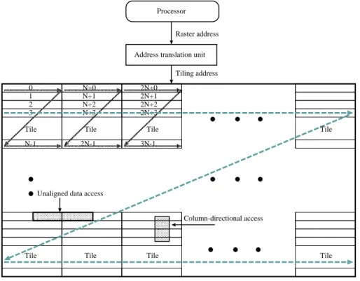
To reduce the address calculation overhead of the software-based tiling, a hardware-
based cache tiling structure for morphological image processing was proposed by Wit-
tenbrink and Somani. They showed that the hardware-based tiling approach has three important advantages over the software approach: 1) The image storing and transfer mechanisms, such as direct memory access (DMA) or I/O devices, are independent of the tiling scheme. 2) A small tile can be used to process images of arbitrary size, and, most importantly, 3) The address translation is transparent to the user software. These advantages are based on the address translation taking place in hardware, and not in software. As shown in Figure 2.9, by address bit-order interchange, the hardware-based address translation unit translates a raster address (logic address) from an external pro- cessor into a tiling address (virtual address) to access data in memory. At a result, the address bit-order interchange eliminates the tiling address calculation overhead and allow the tiling data of virtual address space to be accessed as conventional raster data of logic address space.
Address translation unit Raster address Processor
0 1 2 3
N-1
N+0 N+1 N+2 N+3
2N-1 Tile
2N+0 2N+1 2N+2 2N+3
3N-1
Tile Tile Tile
Tile Tile
Tile Tile
Unaligned data access
Column-directional access Tiling address
Figure 2.9: Hardware-based tiling.
Compared with the software-based tiling, unaligned row-directional access can be
easily realized because the address translation is transparent to the user software. How-
ever, this conventional address translation unit has a drawback, that is each width of the 2-D processing area requires a different address bit-order interchange. For appli- cations such as MM, if the width of the 2-D processing area is not fixed, a different address bit-order interchange is required for the width when the matrix size changes.
For example, if the matrix size is 128, the width of the 2-D processing area is set at 128. This complex address translation can avoid mapping the waste space of the 2-D data processing area. However, it increases hardware scale of the address translation and may cause a clock-cycle constraint problem.
2.2.2.3 Problem of the cache tiling method
Software-based tiling and hardware-based tiling method improve the 2-D reference locality and reduce the cache capacity misses efficiently. However, there are several problems remain to be solved:
• It cannot support parallel aligned/unaligned data access in both row and column direction.
• Conventional tiling only provides a major-directional access capability. 2-D data processing by SIMD operations is restricted by no availability of non-major- directional parallel access function so that it cannot avoid performance degra- dation caused by the ineffective non-major-directional access. In addition, the transposition processing required in such as DCT or FFT cannot be eliminated.
Transpose operation causes a significant processing overhead.
• Conventional tiling improves the 2-D reference locality and reduce capacity misses efficiently. However, it is inefficient for reducing TLB misses because the non- major directional access causes frequent TLB misses for large-sized 2-D data access.
• For conventional hardware-based tiling, each width of the 2-D processing area
requires a different address bit-order interchange. This complex address trans-
lation not only increases the hardware scale of address translation and but also
may cause a clock-cycle constraint problem.
• Conventional tiling cannot support simultaneous parallel small tile access. As a result, it cannot provide efficient 2-D unit block access so that excessive data transfer problem remains to be solved for image processing and video coding.
2.2.3 Hardware prefetching
In addition to the previously discussed method of cache tiling, many modern processors now uses hardware prefetching techniques to improve the performance of execution of applications [24]. Hardware prefetching is a technique used by processors that predicts soon-to-be used instructions or data and loads them from their original low-speed main memory into the high-speed cache memory before they are accessed. Prefetching has been used as an effective technique to improve the cache behavior of conventional raster layout by reducing memory access latency.
Hardware prefetching keeps track of memory access patterns, and fetches cache lines that may be accessed based on the memory access pattern in the future. There are several kinds of hardware prefetching methods. A commonly used method is sequential unit-stride prefetching, where cache lines are accessed with stride of one. For example, if the processor contiguously accesses the cache lines of A, A+1 and A+2, the prefetcher can predict that A+3 will be accessed next, and starts fetching the cache line of A+3.
Listing 2: The basic MM version (ikj).
1
int main ()
2
{
3
for ( i = 0; i < N ; i ++)
4
for ( k = 0; k < N ; k ++)
5
for ( j = 0; j < N ; j ++)
6
C [ i ][ j ]+= A [ i ][ k ] * B [ k ][ j ];
7
}
Another commonly used method of hardware prefetching is called constant-stride
prefetching, which is similar to sequential unit-stride prefetching, but with variable
access stride (not always + 1). For example, if the processor contiguously accesses
the cache lines of A, A+100 and A+200, the constant-stride prefetcher can detect
the memory access pattern and start fetching the cache line of A+300. Consider the MM given in Listing 2. All arrays in Listing 2 can be prefetched by using sequential unit-stride prefetching, because all of them are accessed in the major direction of the row-major layout.
There are significant cases where sequential unit-stride prefetching cannot be used.
Consider the MM given in Listing 3. Array A[i][k] can be prefetched in the innermost loop by using the sequential unit-stride prefetch because the sequential accesses in the row direction fits into the sequential unit-stride pattern. However, array B[k][j] cannot be prefetched by using the sequential unit-stride prefetch because the sequential access of array B[k][i] is oriented in the non-major column direction. The access pattern would be B, B+N, B+2N, and so on, which cannot be detected by the sequential unit-stride prefetcher.
Listing 3: The basic MM version (ijk).
1
int main ()
2
{
3
for ( i = 0; i < N ; i ++)
4
for ( j = 0; j < N ; j ++)
5
for ( k = 0; k < N ; k ++)
6
C [ i ][ j ]+= A [ i ][ k ] * B [ k ][ j ];
7