Solution‑Deposited at Near Room Temperature for Rigid or Flexible Perovskite Solar Cells with High Efficiencies
Author Qingshun Dong, Jiangwei Li, Yantao Shi, Min Chen, Luis K. Ono, Ke Zhou, Chunyang Zhang, Yabing Qi, Yuanyuan Zhou, Nitin P. Padture, Liduo Wang
journal or
publication title
Advanced Energy Materials
volume 9
number 26
page range 1900834
year 2019‑05‑28
Publisher John Wiley & Sons, Inc.
Rights (C) 2019 WILEY‑VCH Verlag GmbH & Co. KGaA, Weinheim
This is the accepted version of the following article: Dong, Q., Li, J., Shi, Y., Chen, M., Ono, L. K., Zhou, K., Zhang, C., Qi, Y., Zhou, Y., Padture, N. P., Wang, L., Improved SnO2 Electron Transport Layers Solution‐Deposited at Near Room Temperature for Rigid or Flexible Perovskite Solar Cells with High Efficiencies.
Adv. Energy Mater. 2019, 9, 1900834, which has been published in final form at
https://doi.org/10.1002/aenm.201900834. This article may be used for non‑commercial
purposes in accordance with the Wiley Self‑Archiving Policy
[https://authorservices.wiley.com/authorresour ces/Journal‑Authors/licensing/self‑archiving.h tml].
Author's flag author
URL http://id.nii.ac.jp/1394/00001198/
doi: info:doi/10.1002/aenm.201900834
1 DOI: 10.1002/ ((please add manuscript number)) Article type: Full Paper
Surface-Absorbed Water Mediated in situ Recrystallization of SnO2 Electron Transport Layer near Room Temperature for High Efficiency Perovskite Solar Cells
Qingshun Dong, Jiangwei Li, Yantao Shi,* Min Chen, Luis K. Ono, Yabing Qi, Yuanyuan Zhou, Nitin P. Padture,* and Liduo Wang*
Q. S. Dong, J. W. Li and Prof. L. D. Wang
Key Lab of Organic Optoelectronics, Molecular Engineering of Ministry of Education, Department of Chemistry, Tsinghua University, Beijing, 100084, China
*Email: [email protected] Prof. Y. T. Shi
State Key laboratory of Fine Chemicals, School of Chemistry, Dalian University of Technology, Dalian, 116024, China
*Email: [email protected]
M. Chen, Prof. Y. Y. Zhou and Prof. N. P. Padture
School of Engineering, Brown University, Providence, Rhode Island, 02912, United States
*Email: [email protected] Dr. L. K. Ono, and Prof. Y. B. Qi
Energy Materials and Surface Sciences Unit, Okinawa Institute of Science and Technology Graduate University, Okinawa, 904-0495, Japan
Keyword: tin dioxide, room temperature, recrystallization, morphological control, perovskite solar cells
Abstract
Electron transport layer (ETL) is a functional layer of great significance for boosting the power conversion efficiency (PCE) of perovskite solar cells (PSCs). To date, it is still a challenge to simultaneously reduce the surface defects and improve the crystallinity of ETL
2
during low-temperature processing of ETLs. Here, we report a novel strategy for the mediation of in situ recrystallization of SnO2 ETLs, by introducing controlled trace amounts of surface absorbed water on the fluorinated tin oxide (FTO) or indium-tin-oxide (ITO) surfaces of the substrates using ultraviolet ozone (UVO) pretreatment. The optimum amount of adsorbed water plays a key role in balancing the hydrolysis-condensation reactions during the structural evolution of SnO2 thin films. This new approach results in full-coverage SnO2
ETL with a desirable morphology and crystallinity for superior optical and electrical properties, as compared to the control SnO2 ETL without the UVO pretreatment. Finally, the rigid and flexible PSC devices based on our new SnO2 ETLs yield high PCEs of up to 20.5%
and 17.5%, respectively.
Introduction
Organic-inorganic halide perovskites (OIHPs) have recently emerged as a new class of semiconductor material with outstanding characteristics, such as facile solution-processibility, moderate band-gap, strong light-absorption, ultralong carrier-lifetime, etc. These characteristics of thin-film OIHPs make them highly versatile, with great potential for use in solar cells, light-emitting diodes (LEDs), photodetectors, and other applications.[1-4] In particular, the record power conversion efficiency (PCE) of perovskite solar cells (PSCs) has seen an extraordinary rise to nearly 24% within a relatively short period of time.[5-8] The electron transport layer (ETL) within the multilayer PSCs is of great significance as it performs the key role of extracting and transporting photo-generated electrons. In fact, some of the key advances in PSCs and their stability have been the result of advances in ETL materials and/or structures.[9-13] An ideal ETL should have full coverage, high electronic conductivity (n-type), and few surface trap states, as well as favorable band alignment and intimate contact with the adjacent light-absorber OIHP layer.[14] One of the advantages of
3
thin-film PSCs is that they can also be made to be flexible for possible consumer applications.
Thus, low-temperature (<150 °C) deposition of ETLs, compatible with plastic substrates, becomes a requirement.[15]
While TiO2 is the most widely used ETL material, recently SnO2 has proven to be an excellent ETL material, and it is being used more frequently in PSCs with PCEs exceeding 20%.[16-19] In addition to the high chemical stability and low-temperature processability, SnO2
has higher electronic conductivity, wider band gap, and excellent optical transparency compared to TiO2.[11] Also, SnO2 ETL has been found to have better band alignment, with some of the state-of-art OIHP compositions, as compared to TiO2 ETL.[11, 20-21] Furthermore, unlike TiO2, SnO2 does not photo-catalyze the undesirable decomposition of the OIHP layer under solar ultraviolet (UV) irradiation.
Since 2015, the groups of Fang and Yan have jointly conducted extensive research on SnO2-based ETLs, and they have reported some novel strategies for their low-temperature fabrication, nanostructure development, and electrical-properties tuning.[22] Very recently, they obtained a high PCE of 20.8% through precise control of the carrier concentration in an ETL based on SnO2 quantum dots (QDs).[18] In addition, Hagfeldt and co-workers have fabricated SnO2 layers by chemical-bath deposition, and obtained a high PCE of 20.8%.[17]
Meanwhile, a certified record PCE of 20.9% has been achieved by You and co-workers, whose PSCs with planar architecture had an ETL based on SnO2 nanoparticles.[19] However, a few key issues regarding SnO2 ETL still remain unresolved. For example, enhancing the crystallinity and eliminating surface defects in SnO2 ETLs still requires high-temperature heat-treatments (>180 °C). While post-deposition UV-ozone (UVO) is an effective treatment to eliminate surface defects in oxide ETLs at near room temperature, that treatment is ineffective in improving the inherent poor crystallinity of ETLs deposited using low- temperature methods.[17, 23-24] Thus, it is difficult to reduce the surface-defects concentration in
4
SnO2 ETL, enhance its crystallinity, and tune the surface roughness simultaneously during low-temperature processing.
Here we elucidate a new approach where UVO pretreatment of fluorinated-tin-oxide (FTO) or indium-tin-oxide (ITO) substrate surfaces before the deposition of the SnO2 ETLs generates absorbed water molecules in situ. During subsequent room-temperature sol-gel deposition of SnO2 nanocrystallites on the UVO-pretreated substrates, the optimum amount of surface-adsorbed water molecules facilitates optimal hydrolysis-condensation reactions for the recrystallization of SnO2. This results in full-coverage SnO2 ETL with a desirable morphology and crystallinity for superior optical and electrical properties, as compared to the control SnO2 ETL without the UVO pretreatment. Also, the new SnO2 ETL has an optimum roughness, which promotes better interfacial electrical coupling with the subsequently solution-deposited OIHP layer. Thus, the resulting improved charge-transfer dynamics yield high PCEs, up to 20.5% (with a steady-state output of 20.1%), in PSCs. Taking advantage of the low-temperature processability, fabrication of flexible PSCs incorporating the new high quality SnO2 ETL on plastic substrates with a high PCE of 17.5% is also demonstrated.
Results and Discussion
UVO is commonly used as a surface-cleaning method that can remove organic residue from substrate surfaces effectively, and increase the surface wettability.[25] Thus, it is assumed that water from the atmosphere (~50% RH) will adsorb more readily on UVO-pretreated FTO substrates, as illustrated schematically in Figure 1a. As it will be shown later, the amount of surface-adsorbed water depends on the UVO-pretreatment duration, which becomes a critical parameter for controlling the quality of the subsequently deposited SnO2 ETL. Figure 1b shows Fourier transform infrared (FTIR) spectra of FTO-coated glass substrates as a function of UVO-pretreatment duration, where the intensity of the band associated with vibration of
5
hydrogen-containing bonds gradually increases with the UVO-pretreatment duration (0 to 40 min). At the same time, the band position shifts from ~3650 cm-1 (t = 0 min) to ~3350 cm-1 (t
= 40 min), indicating the formation of intermolecular hydrogen bonds because of more surface-absorbed water molecules.[26] The relative amount of adsorbed water is estimated from Figure 1b, and it is plotted in Figure 1c. (As a reference, the band associated with the underlying glass remains unchanged in Figure 1b.) Thus, the FTIR results indicate that prolonged UVO pretreatment can effectively increase the adsorbed surface-water content on FTO, and hydrogen bonds are inclined to form as more water molecules are absorbed onto the FTO surface.
The SnO2 sol used for the following spin-coating was prepared according to our previous work, which contains SnO2 nanocrystallines (<5 nm) dispersed in anhydrous alcohol.[24] The SnO2 sol was spin-coated onto the UVO-pretreated FTO substrates for 0-40 min at a fixed ambient humidity (~50% RH). The SnO2 ETLs were subsequently heat-treated at 50 °C for 2 h in air, followed by a 20-min UVO post-treatment. Thus, the only parameter varied here is the UVO-pretreatment duration. Here, our samples are marked using “S-X”, where “X”
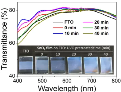
represents the duration time of UVO-pretreatment (min). The transmittance spectra and photographs in Figure S1 show that the two samples of S-10 and S-20 have higher transmittance compared to the bare FTO substrate, consistent with a previous report on the anti-reflection effect of the SnO2 films.[27] However, the ETLs begin to become foggy and the transmittance gets decreased as the UVO-pretreatment duration exceeds 20 min, indicating that the UVO-pretreatment has a notable effect on the SnO2 ETL optical characteristics.
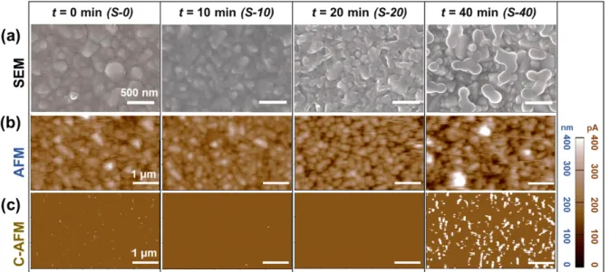
Scanning electron microscopy (SEM) results are presented in Figure 2a, showing the surface morphology and topography of SnO2 ETLs on FTO substrates as a function of UVO- pretreatment duration. Some small cracks and pinholes can be seen in the film without UVO pretreatment (Figure 2a, t = 0 min). The small amount of organic residue that is omnipresent
6
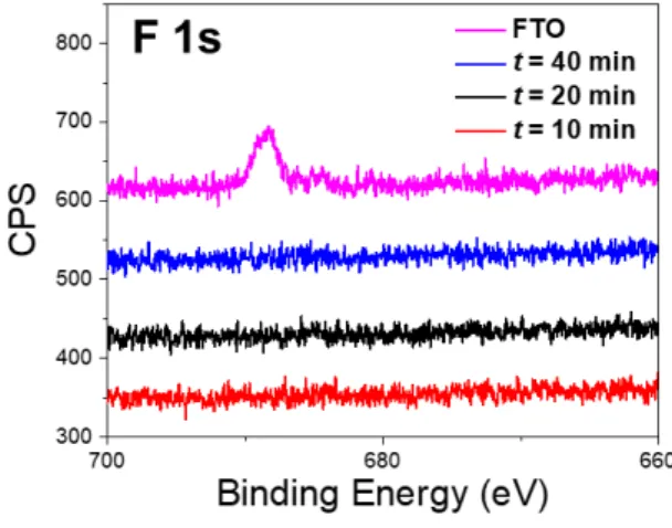
on the FTO surface before UVO pretreatment can cause poor substrate surface wetting, which can result in the formation of the cracks/pinholes and high roughness during annealing (see Figure S2 for variation of film roughness with UVO-pretreatment duration). In contrast, the cracks/pinholes have disappeared in S-10, resulting in a compact, full-coverage thin film with low roughness. Longer UVO pretreatment, for example in the case of S-20, causes an increase in surface roughness, while further UVO pretreatment (t = 40 min) results in films with agglomerated SnO2 grains and incomplete coverage. The AFM results (Figure 2b) are consistent with what is observed in the SEM. The conductive AFM (C-AFM) results in Figure 2c clearly show the underlying FTO substrate as high conductivity bright regions in all images except S-20. This confirms full SnO2 ETL coverage for UVO-pretreatment duration of 10 and 20 min. Fluorine (F) 1s X-ray photoelectron spectroscopy (XPS) on these SnO2 ETLs were also performed, but the results are inconclusive (Figure S3). This is most likely because the XPS detection depth is <10 nm, whereas C-AFM detection depth is >50 nm.
The two samples of S-10 and S-20 were further characterized, and the Hall-effect mobility of S-20 is 45.3 cm2·V-1·s-1, which is three times higher than that of S-10 (15.8 cm2·V-1·s-1).
Also, in specimens where the OIHP thin film is deposited on top of the SnO2 ETLs (described later), there are gaps at the interface between the OIHP thin film and the SnO2 ETL (S-10), as shown in the cross-sectional SEM images in Figure S4. In contrast, in the case using S-10 ETL there is no such gaps (Figure S4) while the interface roughness is relatively high (Figure S2), which could be advantageous in providing maximum electrical contact between the two layers.[28-29] These results show clearly that there is an optimum UVO-pretreatment duration, which in turn induces the adsorption of an optimum amount of water on the FTO substrate that controls the development of the most desirable SnO2 ETL microstructure and morphology. Henceforth, the S-10 ETL is considered as the ‘reference’ film, and the S-20
7
ETL is considered as the ‘optimum’ film, for a fair comparison as both ETLs are full- coverage.
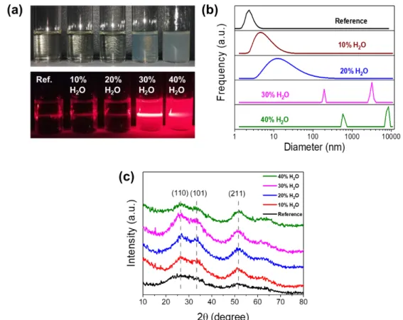
To demonstrate the key role water concentration plays in the sol-gel synthesis of SnO2, we have performed some model experiments. Here, different amounts of water (10%, 20%, 30%, and 40% in volume) were added to a stable SnO2 sol, and the results are summarized in Figure S5. Although there is no obvious variation in the appearance of the sol (see photographs in Figure S5a) with 10% and 20% water, the dynamic light scattering (DLS) results (Figure S5b) show that the average colloidal-particles size has increased from ~3 nm (0% water) to ~5 nm (10% water) to 10-20 nm (20% water). With the addition of more water (30% and 40%), the sol becomes translucent and turbid, with the bimodal particle sizes reach several hundred nanometers and few microns. These sols were dried at room temperature, and they were characterized using X-ray diffraction (XRD). The results (Figure S5c) indicate that the water did not promote the formation of any new phases, but its main effect is on the crystallinity of the SnO2 particles. After a certain amount of added water (<30%) into the sol, the SnO2 110 and 101 XRD peaks develop, indicating an increase in the SnO2 crystallinity.
Dried powders from original SnO2 sol and with 20% added water were characterized using transmission electron microscopy (TEM). The results (Figure S6) show an increase in the SnO2 particle size and enhanced crystallinity, which is consistent with the DLS and XRD results. These results confirm that optimum water concentration is needed to obtain desirable crystallinity and size in SnO2 particles.
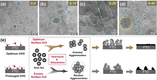
It is argued that, in the case of sol-gel deposition of SnO2 ETL using spin-coating, a similar optimum amount of water on UVO-pretreated substrates is needed for obtaining high crystallinity and control over the particle size as well as surface roughness. It is suggested that the hydrolysis of the SnO2 sol is inadequate if the amount of adsorbed water on the substrate is deficient (t = 0-10 min), resulting in small SnO2 particles with poor crystallinity. This is
8
confirmed by TEM characterization of freshly spin-coated SnO2 ETL (without the 50 °C-heat- treatment or UVO post-treatment) scraped from the substrate (Figs. 3a and 3b). However, the hydrolysis and condensation reactions occur in a balanced way when there is moderate amount of adsorbed water (in the case of S-20),[30]which can promote oriented attachment of the tiny SnO2 nanocrystallites during recrystallization resulting in higher crystallinity.[26] The TEM image in Figure 3c (S-20) shows evidence for larger SnO2 particles with relatively high crystallinity. However, when there is excess adsorbed water (for example, in the case of S-40), the hydrolysis reaction is likely to occur more rapidly, resulting in randomly agglomerated nanoparticles, as evidenced in the TEM image in Figure 3d. Figure 3e is a schematic illustration of the proposed mechanism.
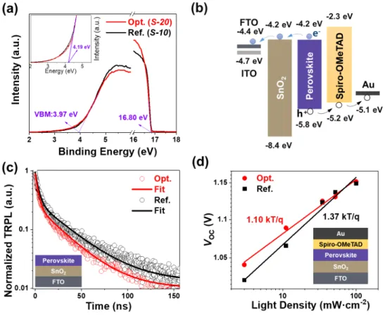
Although methylammonium lead triodide (CH3NH3PbI3 or MAPbI3) is the most widely studied OIHP for solar cells, the mixed-composition OIHPs, such as Cs0.05(FA0.85MA0.15)0.95Pb(I0.85Br0.15)3, have been shown to be more suitable light absorbers, and they are also more stable.[31] However, the relatively deeper conduction band minimum (CBM) level (-4.2 eV) of this OIHP (valence band maximum or VBM level -5.8 eV; band gap 1.6 eV) makes TiO2 ETL unsuitable for PSCs,[32] whereas SnO2 is ideally suited for efficient electron extraction.[20] Here, we have measured the energy levels of the bands of the reference SnO2 ETL (S-10) and the optimum SnO2 ETL (S-20) using ultraviolet photoemission spectroscopy (UPS) and UV-vis absorption. As shown in the inset of Figure 4a, the optical band gap (Eg) is estimated to be ~4.2 eV. The cutoff energy in Figure 4a is ~16.8 eV, and the Fermi level is ~4.0 eV below the vacuum level. This results in the VBM level of -8.4 eV (considering photon energy of He-Ia excitation to be 21.2 eV) and the CBM level of -4.2 eV (considering Eg of ~4.2 eV). The energy-level diagram is presented in Figure 4b, showing good band alignment for electron and hole transfer, with
9
Cs0.05(FA0.85MA0.15)0.95Pb(I0.85Br0.15)3 composition OIHP which is used in the rest of this study.
While the band structures of the reference and the optimum SnO2 ETLs are similar, the charge-transfer dynamics and trap-assisted recombination are improved in the optimum SnO2
ETL, as shown in Figs. 4c and 4d. Time-resolved photoluminescence (TRPL) results on devices with OIHP layer deposited on top of the optimum SnO2 ETL in Figure 4c reveal rapid decay, with carrier (electrons) lifetimes of τ1 = 3.0 ns and τ2 = 28.0 ns (two-parameters curve fitting). In comparison, the reference SnO2 ETL carrier lifetimes are somewhat longer: τ1 = 3.4 ns and τ2 = 31.9 ns, suggesting less efficient electrons quenching by that ETL. Full PSC devices with n-i-p architecture, FTO/SnO2/Cs0.05(FA0.85MA0.15)0.95Pb(I0.85Br0.15)3/Spiro- OMeTAD/Au, were also fabricated. Figure 4d is a semi-logarithmic plot of the measured VOC
of the PSCs as a function of incident light intensity, showing near-ideal kT/q slope of 1.1 indicating reduced trap-assisted recombination in the PSC with the optimum SnO2 ETL (slope is 1.37 for PSC with the reference SnO2 ETL). The improved properties of the optimum SnO2
ETL are attributed to its improved crystallinity and larger grain size.
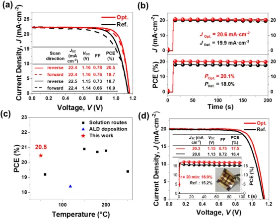
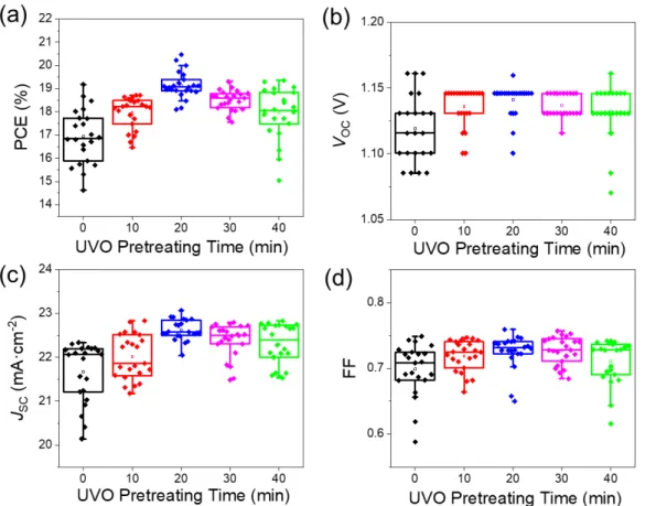
The PV performance of PSCs with SnO2 ETLs on FTO substrates UVO-pretreated for t = 0, 10, 20, 30, or 40 min were measured. The PV-performance data and statistics are presented in Figure S7, and they are summarized in Table S1. These results indicate clearly that optimum UVO-pretreatment, for optimum amount of adsorbed water on FTO substrates, gives the best SnO2 ETL for maximum PV performance. Figure 5a presents current density-voltage (J-V) curves and the extracted PV-performance data (inset table) for ‘champion’ PSCs with reference and optimum SnO2 ETLs. Although both PSCs show hysteresis, it is much more pronounced in the reference PSC. Both PSCs have similar short-circuit current density (JSC) values (22.4 to 22.5 mA·cm-1, reverse scan), but the open-circuit voltage (VOC) of the PSC with optimum ETL (1.16 V, reverse scan) is somewhat higher, and the fill factor (FF) is
10
significantly improved (0.78, reverse scan). The highest PCE of the PSC with optimum ETL is 20.5% (reverse scan) compared to 18.7% for the PSC with reference ETL. Maximum power-point J and PCE for PSCs with reference and optimum ETL are plotted in Figure 5b, showing steady PV performance. The J-V responses of other PSCs with reference and optimum SnO2 ETLs are presented in Figure S8a, which also show a similar trend. The external quantum efficiency (EQE) and the integrated JSC data are presented in Figure S8b, where the JSC measured from the J-V curve (22.4 mA·cm-2, reverse scan) is consistent with that from EQE spectrum (21.8 mA·cm-2) for the optimum PSC. The average series (RS) and shunt (RSH) resistance values of the PSC with reference ETL were measured to be 7.1 Ω·cm2 and 5573 Ω·cm2, respectively, whereas they are 5.5 Ω·cm2 and 6182 Ω·cm2, respectively, for the PSC with optimum ETL. The simultaneous decrease in RS and an increase in RSH suggests improved charge-transfer dynamics in the PSC with optimum SnO2 ETL, which appears to be responsible for the overall improved PV performance.
It has been shown that trapped charge can induce irreversible degradation of OIHPs,[9, 33]
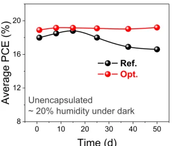
and both the presence of trap states at the ETL/OIHP interface and the low charge mobility of the ETL could impede the electron transfer. Therefore, it is reasonable to speculate that improved charge transport and reduced trap state density between the optimum SnO2 ETL and the OIHP layer can result in a more stable device. To verify this hypothesis, unencapsulated PSCs with reference and optimum SnO2 ETLs were stored at room temperature in a desiccator (humidity <20%) in dark, and their PCEs were measured in ambient atmosphere about every 5 days. As shown in Figure S9, after 50 days of storage, PSC with optimum SnO2
ETLs shows almost no degradation, whereas the PCE of the PSC with reference SnO2 ETLs has degraded to 90% of the original value.
We also put this work in the context of other studies, Figure 5c plots maximum PCE achieved against the highest temperature needed for the deposition of SnO2 ETLs in PSCs.[17-
11
18, 20, 34-36] It can be clearly seen that the temperature for tuning the ETL crystallinity and microstructure in this work is the lowest among these relevant researches. Thus, taking advantage of the low-temperature (50 °C) processing of high quality SnO2 ETLs, flexible PSCs on plastic substrates (polyethylene naphthalate or PEN with indium tin oxide or ITO) were fabricated with reference or optimum SnO2 ETL (same PSC architecture as above).
Figure 5d presents the J-V curves and PV-performance data for the ‘champion’ PSCs, showing 17.5% maximum PCE (16.9% steady-state PCE) using optimum SnO2 ETL, compared with 16.9 % maximum PCE (15.4% steady-state PCE) using reference SnO2 ETL.
The >17% PCE is comparable to PCEs of state-of-the-art flexible PSCs.[37]
Conclusions
In conclusion, for the, we have demonstrated a new strategy for simultaneously tuning the crystallinity, density of trap states, and surface roughness in SnO2 ETL used in PSCs at near room temperature. The key of this new method is the regrowth of SnO2 nanocrystallines triggered by the water absorbed on the FTO or ITO surfaces introduced by UVO pretreatment.
It was found that the amount of water is a critical factor for obtaining high quality SnO2 ETLs through balanced hydrolysis-condensation reactions. As compared to control SnO2 ETL, our new SnO2 ETL have improved optical and electrical properties. Also, a relatively rough surface ensured that the new SnO2 ETL bonds tightly with perovskite layer, providing good interfacial electrical coupling. The structural advantages of the new ETL results in an improvement in charge transfer dynamics, by which the energy loss within PSCs is further minimized, and a notable enhancement in PCE is achieved as a result. Finally, PSC devices based on our new SnO2 ETL show high PCEs up to 20.5%, with a steady-state output of 20.1%. In the case of flexible PSC, a high PCE of 17.5% is obtained using the new SnO2 ETL.
12 Supporting Information
Supporting Information is available from the Wiley Online Library or from the author.
Acknowledgements
This research was funded primarily by the National Natural Science Foundation of China (Grant No. 91433205, 51773025) and the Fundamental Research Funds for the Central Universities (Grant No. DUT18ZD208). The work at Brown University was funded by the US National Science Foundation (OIA-1538893). L.K.O. and Y.B.Q. acknowledge the funding support from the Energy Materials and Surface Sciences Unit of the Okinawa Institute of Science and Technology Graduate University, the OIST Proof of Concept (POC) Program, the OIST R&D Cluster Research Program, and JSPS KAKENHI Grant Number JP18K05266.
The authors are grateful to M. Shen for his assistance with the TEM characterization.
Received: ((will be filled in by the editorial staff)) Revised: ((will be filled in by the editorial staff)) Published online: ((will be filled in by the editorial staff)) References
[1] M. Chen, M.-G. Ju, M. Hu, Z. Dai, Y. Hu, Y. Rong, H. Han, X. C. Zeng, Y. Zhou, N. P. Padture, ACS Energy Letters 2019, 4, 276.
[2] M. V. Kovalenko, L. Protesescu, M. I. Bodnarchuk, Science 2017, 358, 745.
[3] Y. Liu, Y. Zhang, Z. Yang, H. Ye, J. Feng, Z. Xu, X. Zhang, R. Munir, J. Liu, P. Zuo, Q. Li, M. Hu, L.
Meng, K. Wang, D.-M. Smilgies, G. Zhao, H. Xu, Z. Yang, A. Amassian, J. Li, K. Zhao, S. Liu, Nat.
Commun. 2018, 9, 5302.
[4] M. Chen, M.-G. Ju, A. D. Carl, Y. Zong, R. L. Grimm, J. Gu, X. C. Zeng, Y. Zhou, N. P. Padture, Joule 2018, 2, 558.
[5] M. M. Lee, J. Teuscher, T. Miyasaka, T. N. Murakami, H. J. Snaith, Science 2012, 338, 643.
[6] H.-S. Kim, C.-R. Lee, J.-H. Im, K.-B. Lee, T. Moehl, A. Marchioro, S.-J. Moon, R. Humphry-Baker, J.-H. Yum, J. E. Moser, Sci. Rep. 2012, 2, 591.
[7] J.-W. Lee, Z. Dai, C. Lee, H. M. Lee, T.-H. Han, N. De Marco, O. Lin, C. S. Choi, B. Dunn, J. Koh, D.
Di Carlo, J. H. Ko, H. D. Maynard, Y. Yang, J. Am. Chem. Soc. 2018, 140, 6317.
[8] N. J. Jeon, H. Na, E. H. Jung, T.-Y. Yang, Y. G. Lee, G. Kim, H.-W. Shin, S. Il Seok, J. Lee, J. Seo, Nat.
Energy 2018, 3, 682.
13
[9] H. Tan, A. Jain, O. Voznyy, X. Lan, F. P. García de Arquer, J. Z. Fan, R. Quintero-Bermudez, M.
Yuan, B. Zhang, Y. Zhao, F. Fan, P. Li, L. N. Quan, Y. Zhao, Z.-H. Lu, Z. Yang, S. Hoogland, E. H.
Sargent, Science 2017, 355, 722.
[10] S. S. Shin, E. J. Yeom, W. S. Yang, S. Hur, M. G. Kim, J. Im, J. Seo, J. H. Noh, S. I. Seok, Science 2017, 356, 167.
[11] Q. Jiang, L. Zhang, H. Wang, X. Yang, J. Meng, H. Liu, Z. Yin, J. Wu, X. Zhang, J. You, Nat. Energy 2016, 2, 16177.
[12] B. Roose, Q. Wang, A. Abate, Adv. Energy Mater. 2019, 9, 1803140.
[13] M. M. Tavakoli, P. Yadav, R. Tavakoli, J. Kong, Adv. Energy Mater. 2018, 8, 1800794.
[14] L. Xiong, Y. Guo, J. Wen, H. Liu, G. Yang, P. Qin, G. Fang, Adv. Funct. Mater. 2018, 28, 1802757.
[15] Y. Wang, S. Bai, L. Cheng, N. Wang, J. Wang, F. Gao, W. Huang, Adv. Mater. 2016, 28, 4532.
[16] Q. Dong, Y. Shi, K. Wang, Y. Li, S. Wang, H. Zhang, Y. Xing, Y. Du, X. Bai, T. Ma, J. Phys. Chem. C 2015, 119, 10212.
[17] E. H. Anaraki, A. Kermanpur, L. Steier, K. Domanski, T. Matsui, W. Tress, M. Saliba, A. Abate, M.
Grätzel, A. Hagfeldt, J.-P. Correa-Baena, Energy Environ. Sci. 2016, 9, 3128.
[18] G. Yang, C. Chen, F. Yao, Z. Chen, Q. Zhang, X. Zheng, J. Ma, H. Lei, P. Qin, L. Xiong, W. Ke, G. Li, Y. Yan, G. Fang, Adv. Mater. 2018, 30, e1706023.
[19] Q. Jiang, Z. Chu, P. Wang, X. Yang, H. Liu, Y. Wang, Z. Yin, J. Wu, X. Zhang, J. You, Adv. Mater.
2017, 29, 1703852.
[20] J. P. Correa Baena, L. Steier, W. Tress, M. Saliba, S. Neutzner, T. Matsui, F. Giordano, T. J.
Jacobsson, A. R. Srimath Kandada, S. M. Zakeeruddin, A. Petrozza, A. Abate, M. K. Nazeeruddin, M. Grätzel, A. Hagfeldt, Energy Environ. Sci. 2015, 8, 2928.
[21] Q. Dong, Y. Shi, C. Zhang, Y. Wu, L. Wang, Nano Energy 2017, 40, 336.
[22] W. Ke, G. Fang, Q. Liu, L. Xiong, P. Qin, H. Tao, J. Wang, H. Lei, B. Li, J. Wan, G. Yang, Y. Yan, J. Am.
Chem. Soc. 2015, 137, 6730.
[23] M. Park, J.-Y. Kim, H. J. Son, C.-H. Lee, S. S. Jang, M. J. Ko, Nano Energy 2016, 26, 208.
[24] Q. S. Dong, Y. T. Shi, C. Y. Zhang, Y. K. Wu, L. D. Wang, Nano Energy 2017, 40, 336.
[25] W. Ke, G. Fang, J. Wan, H. Tao, Q. Liu, L. Xiong, P. Qin, J. Wang, H. Lei, G. Yang, M. Qin, X. Zhao, Y.
Yan, Nat. Commun. 2015, 6, 6700.
[26] T. L. Tso, E. K. Lee, The Journal of Physical Chemistry 1985, 89, 1612.
[27] L. Xiong, M. Qin, G. Yang, Y. Guo, H. Lei, Q. Liu, W. Ke, H. Tao, P. Qin, S. Li, H. Yu, G. Fang, J.
Mater. Chem. A 2016, 4, 8374.
[28] D. Liu, S. Li, P. Zhang, Y. Wang, R. Zhang, H. Sarvari, F. Wang, J. Wu, Z. Wang, Z. D. Chen, Nano Energy 2017, 31, 462.
[29] M. M. Tavakoli, P. Yadav, R. Tavakoli, J. Kong, Adv. Energy Mater. 2018, 8, 1800794.
[30] R. L. Penn, J. F. Banfield, Science 1998, 281, 969.
[31] M. Saliba, T. Matsui, J.-Y. Seo, K. Domanski, J.-P. Correa-Baena, M. K. Nazeeruddin, S. M.
Zakeeruddin, W. Tress, A. Abate, A. Hagfeldt, Energy Environ. Sci. 2016, 9, 1989.
[32] C. Zhang, Y. Shi, S. Wang, Q. Dong, Y. Feng, L. Wang, K. Wang, Y. Shao, Y. Liu, S. Wang, J. Mater.
Chem. A 2018, 6, 17882.
[33] N. Ahn, K. Kwak, M. S. Jang, H. Yoon, B. Y. Lee, J.-K. Lee, P. V. Pikhitsa, J. Byun, M. Choi, Nat.
Commun. 2016, 7, 13422.
[34] D. Yang, R. Yang, K. Wang, C. Wu, X. Zhu, J. Feng, X. Ren, G. Fang, S. Priya, S. F. Liu, Nat. Commun.
2018, 9, 3239.
[35] Q. Jiang, Z. Chu, P. Wang, X. Yang, H. Liu, Y. Wang, Z. Yin, J. Wu, X. Zhang, J. You, Adv. Mater.
2017, 29, 10.1002/adma.201703852.
[36] K.-H. Jung, J.-Y. Seo, S. Lee, H. Shin, N.-G. Park, J. Mater. Chem. A 2017, 5, 24790.
[37] D. Yang, R. Yang, S. Priya, S. Liu, Angew. Chem. Int. Ed. 2018, DOI: doi:10.1002/anie.201809781.
14
Figure 1. (a) Schematic illustration of the UVO pretreatment and water adsorption on an FTO substrate. (b) FTIR spectra of FTO/glass substrate after UVO pretreatment for different durations. (c) Relative surface water (estimated using the FTIR spectra) as a function of UVO-pretreatment duration.
Figure 2. Top-surfaces of SnO2 ETLs on FTO substrates with UVO pretreatment for t = 0 min, 10 min, 20 min, and 40 min: (a) SEM micrographs, (b) AFM images (‘nm’ scale), and (c) corresponding C- AFM maps (‘pA’ scale).
15
Figure 3. TEM images of freshly spin-coated SnO2 ETL scraped off from FTO substrates that were UVO-pretreated for t =: (a) 0 min, (b) 10 min, (c) 20 min, and (d) 40 min. The turquoise and yellow dashed circles denote single-nanocrystals and clusters, respectively. (e) Schematic illustration of the proposed mechanisms for the structural evolution of SnO2 thin films on FTO substrates with optimum and excess adsorbed water.
16
Figure 4. (a) UPS spectra showing the Fermi edge (left) and cut-off energy (right) of reference (S-10) and optimum (S-20) SnO2 ETLs. Inset: Corresponding UV-vis spectra. (b) Energy levels diagram for the n-i-p PSC device structure. (c) TRPL data for OIHP on reference and optimum SnO2 ETLs (Inset:
device structure schematic). (d) VOC as a function of incident light intensity for PSCs with reference and optimum SnO2 ETLs (inset: device structure schematic).
17
Figure 5. (a) J-V curves and PV parameters (inset), (b) steady-state output of photocurrent and PCE of the champion cells on the reference and 20 min UVO pretreated ETLs; (c) statistics of the current highest performance PSCs on SnO2 ETLs prepared at different temperatures; (d) the champion performance of flexible devices on the reference and 20 min UVO pretreated ETLs.
18 The table of contents entry
We report a novel strategy where controlled FTO surface absorbed water to mediate in situ nanocrystalline regrowth of SnO2 ETLs at room temperature, which gives high PCE of 20.5%
and 17.5% to rigid and flexible PSCs, respectively.
Keyword: tin dioxide, room temperature, recrystallization, morphological control, perovskite solar cells
Q. S. Dong, J. W. Li, Y. T. Shi*, M. Chen, L. K. Ono, Y. B. Qi, Y. Y. Zhou, N. P. Padture,*
L. D. Wang*
Surface-Absorbed Water Mediated in situ Recrystallization of SnO2 Electron Transport Layer near Room Temperature for High Efficiency Perovskite Solar Cells
ToC figure
100 200
18 19 20 21 22
23 SnO2 Electron Transport Layer in Perovskite Solar Cells
Solution routes ALD deposition This work
PCE (%)
ETL Fabrication Temperature (°C) 20.5
1
Supporting Information
Surface-Absorbed Water Mediated in situ Recrystallization of SnO2 Electron Transport Layer near Room Temperature for High Efficiency Perovskite Solar Cells
Qingshun Dong, Jiangwei Li, Yantao Shi,* Min Chen, Luis K. Ono, Yabing Qi, Yuanyuan Zhou, Nitin P. Padture,* and Liduo Wang*
Q. S. Dong, J. W. Li and Prof. L. D. Wang
Key Lab of Organic Optoelectronics, Molecular Engineering of Ministry of Education, Department of Chemistry, Tsinghua University, Beijing, 100084, China
*Email: [email protected]
Prof. Y. T. Shi
State Key laboratory of Fine Chemicals, School of Chemistry, Dalian University of Technology, Dalian, 116024, China
*Email: [email protected].
M. Chen, Prof. Y. Y. Zhou and Prof. N. P. Padture
School of Engineering, Brown University, Providence, Rhode Island 02912, United States
*Email: [email protected]
Dr. L. K. Ono, and Prof. Y. B. Qi
Energy Materials and Surface Sciences Unit, Okinawa Institute of Science and Technology Graduate University, Okinawa, 904-0495, Japan
Experimental Section Materials and Reagents
All the chemicals were used as received, including PbI2 and PbBr2 (>99%, TCI), CH3NH3Br (MABr, Xi’an Polymer Light Technology Corp), NHCHNH2I (FAI, Xi’an Polymer Light Technology Corp), CsI (99.999%, Alfa Aesar), SnCl2·2H2O (98-103%, Alfa Aesar), Spiro-OMeTAD (99.7%, Lumtec Co., Taiwan), ethanol (99.8%, Sinopharm Chemical Reagent Co., Ltd), FK209 (98%, HeptaChroma). 4-tert-butylpyridine (TBP, 96%), Bis (trifluoromethane) sulfonimide lithium salt (99.95%), and solvents acetonitrile (99.9%), dimethylformamide (DMF, 99.8%), dimethylsulfoxide (DMSO, 99.9%), and chlorobenzene (CB, 99.8%) were all purchased from Sigma Aldrich. Fluorinated tin oxide (FTO)-coated glass substrates (7 Ω/sq) and indium tin oxide (ITO)-coated polyethelene naphthalate (PEN) substrates (15 Ω/sq) were purchased from Yingkou OPVtech New Energy Co. Ltd.
SnO2 Sol Preparation
SnCl2·2H2O sol was prepared by dissolving SnCl2·2H2O in anhydrous ethanol (0.1 M) in an open reflux apparatus and stirred at 80 °C for 3 h. After standing at 40 °C for 3 h, the sol was aged for 24 h at room temperature.
SnO2 Electron Transport Layer (ETL) Preparation
FTO/glass or the ITO/PEN substrates were etched with zinc powder and 4 M HCl to obtain the electrode pattern, and then washed with cleaning fluid, deionized water, ethanol (99.7%, Sinopharm), acetone (99.5%, Beijing Shiji), and isopropanol (99.7%, Sinopharm)
2
sequentially. To regulate the crystallinity and morphology of SnO2 films, FTO/glass and ITO/PEN substrates were pretreated with ultraviolet-ozone (UVO) for different duration (0-40 min) under ambient conditions. Subsequently, SnO2 sol was spin-coated on the substrates at 2000 rpm for 30 s, and then heated at 50 °C for 2 h to remove the solvent. For better repeatability, the ambient humidity during UVO-pretreatment and spin-coating was maintained at ~50% RH. All ETLs were then UVO-post-treated for 20 min. The typical thickness of the ETL is 70-100 nm. Finally, the ETL substrates were transferred to the dry air glove box (H2O <0.01 ppm) for Organic-Inorganic Halide Perovskite (OIHP) deposition below.
OIHP Thin Film Preparation
OIHP of composition Cs0.05(FA0.85MA0.15)0.95Pb(I0.85Br0.15)3 was prepared using a procedure described in a previous report.[S1] First, anhydrous mixture of DMF and DMSO (4:1 by volume) containing FAI (1 M), PbI2 (1.1 M), MABr (0.2 M), and PbBr2 (0.22 M) was prepared by stirring at 60 °C for 0.5 h. Subsequently, 50 μL 1.5 M solution of CsI in DMSO was added to the above solution. To prepare the perovskite films, 50 μL solution was spread on the SnO2-ETL/FTO/glass or the SnO2-ETL/ITO/PEN substrates, followed by a two-stage spin-coating processes (1000 rpm for 10 s and 6000 rpm for 20 s). During the second spin coating stage, 100 µL of chlorobenzene were dripped on the spinning substrate 5 s prior the end of spin-coating. Finally, the substrates were annealed at 100 °C for 50 min. This resulted in an OIHP thin film of 600 nm thickness.
Hole Transport Layer (HTL) and Au Electrode Preparation
Precursor solution of HTL was prepared by dissolving 72.3 mg spiro-MeOTAD, 28.8 μL 4-tert-butylpyridine, 17.5 μL lithium bis (trifluoromethylsulphonyl) imide acetonitrile solution (520 mg mL-1) into 1 ml chlorobenzene. Subsequently, HTL was deposited on top of the OIHP layer by spin coating at 3000 rpm for 30 s. Typical thickness of the HTL is ~250 nm. Finally, a 60-nm Au electrode was thermally evaporated on top of the HTL. The active area of the device was 0.16 cm2, as defined by a non-reflective mask.
Characterizations
The size distributions of SnO2 particles were measured using SZ-100Z analyzer (Horiba).
Transmission electron microscopy (TEM) was performed on 2100F (JEOL) instrument using an acceleration voltage of 200 KV. To observe the SnO2 nanoparticles, 20-fold diluted original SnO2 sol (5 μL) was dripped onto holey-carbon TEM grids, and the dried in air at room temperature for 6 h. For the SnO2 ETLs, the as-spin-coated films (without heat-treatment or UVO post-treatment) were scraped off and dispersed in anhydrous ethanol.
About 5 μL of this suspension was dripped onto holey-carbon TEM grids and dried at room temperature for 6 h. Scanning electron microscope (SEM) images were acquired using JSM-7401F (JEOL) and Merlin (Zeiss) field-emission instruments.
Atomic force microscope (AFM) and conducting AFM (C-AFM) images of FTO and SnO2 ETL surfaces were obtained using MFP-3D (Asylum Research) instrument. A conducting Pt-coated Si tip (Econo-SCM-PIC, Asylum Research) was used. All the SnO2 thin films on FTO were connected to the substrate with Ag paste. No bias voltage was applied to obtain the C-AFM images to exclude any possible tunneling effects.
Transmittance Spectra were recorded using U-3900 spectrophotometer (Hitachi).
Photoluminescence (PL) lifetime was measured by FLIM with a FV1200 laser scanning confocal microscope (Olymplus). A 488-nm pulsed diode laser was used for excitation. The emission was filtered through a 50/50 dichroic beam splitter and a 700-800 nm long pass filter.
Fourier transform infrared spectroscopy (FTIR) of the UVO-pretreated FTO substrates were obtained in attenuated total reflection (ATR) mode using V70 spectrometer (Bruker). X-ray
3
photoelectron spectroscopy (XPS) was performed using Kratos Analytical spectrometer (AXIS ULTRA HAS, monochromated Al-Ka = 1486.6 eV) and all XPS spectra were shifted to account for sample charging using inorganic carbon at 284.80 eV as a reference. Ultraviolet photoemission spectroscopy (UPS) was performed using Kratos Analytical spectrometer (AXIS ULTRA DLD), and mono-chromatized He-Ia radiation at 21.2 eV was used.
Hall-effect measurements on the SnO2 ETLs were performed on a device with four-Ga electrode system using 2400 SourceMeter (Keithley).
The current density-voltage (J-V) characteristics of PSCs were measured 2400 SourceMeter (Keithley) at the scan speed of 100 mV s-1 under AM 1.5G one-sun illumination (100 mW·cm-2) generated by an Solar 3A (Oriel) solar simulator. The intensity was calibrated using a VLSI standard incorporated PN 91150V Si reference cell. The PSCs were masked using a black metal mask with a hole area of 0.096 cm2. Steady-state output of current density and PCE were measured using 2400 SourceMeter (Keithley) under a certain bias. The EQE spectra were obtained using IQE 200B quantum efficiency measurement system (Oriel). For long-term stability testing, the devices were stored in the dark in a dry box, and the J-V test was measured regularly.
Supplementary Figures
Figure S1. Transmittance of FTO, and SnO2 ETLs deposited on FTO with different UVO-pretreatment durations. Inset: photographs of the samples (top and bottom dark bands indicate bare glass with the FTO etched away).
4
Figure S2. Roughness variation of the SnO2 ETLs on FTO substrates UVO-pretreated for different durations.
Figure S3. XPS F 1s spectra obtained from the surfaces of bare untreated FTO and SnO2
ETLs on FTO substrates UVO-pretreated for different durations.
Figure S4. Cross-sectional SEM images of perovskite on SnO2 ETLs deposited on FTO substrates UVO-pretreated for 10 min (left) and 20 min (right).
5
Figure S5. (a) Regular images and Tyndall effect of SnO2 sol after added different volume ratio of water; (b) Size distributions of the colloid after adding different water in the sol, determined by dynamic light scattering spectroscopy; (c) XRD results of the powders from the room temperature dried sol with different amount of water in it.
Figure S6. TEM image of (a) the SnO2 nanocrystallines in original sol, (b) the SnO2
nanocrystallines in original sol with 20% H2O added.
5 nm 5 nm
(a) (b)
SnO2Sol SnO2Sol with 20% water
6
Figure S7. Photoelectric performance distribution of the devices on SnO2 ETLs with different UVO pretreatment duration.
Figure S8. Representative J-V curves (a) and corresponding IPCE spectrum (b) of the devices on reference and 20 min UVO pretreated ETLs.
7
Figure S9. Long-term stability measurements of devices without any encapsulation under dark condition.
Supplementary Table
Table S1. Average photovoltaic parameters of PSCs using different ETLs.
UVO Pretreatment
JSC
(mA·cm-2)
VOC
(V) FF PCE
(%)
RS
(W·cm2)
RSH
(W·cm2) t = 0 min 21.67±0.68 1.12±0.03 0.70±0.04 16.94±1.18 6.53±2.61 4786±2905 t = 10 min 22.01±0.51 1.14±0.02 0.72±0.02 17.97±0.69 7.09±1.19 5573±1848 t = 20 min 22.56±0.26 1.15±0.01 0.74±0.02 19.23±0.52 5.46±1.24 6182±791 t = 30 min 22.38±0.39 1.14±0.01 0.73±0.02 18.50±0.42 6.15±0.92 4667±1950 t = 40 min 22.30±0.47 1.13±0.02 0.71±0.03 17.95±1.11 6.47±0.91 4590±1288
Supplementary Reference
[S1] E. H. Anaraki, A. Kermanpur, L. Steier, K. Domanski, T. Matsui, W. Tress, M. Saliba, A. Abate, M. Grätzel, A. Hagfeldt, J.-P. Correa-Baena, Energy Environ. Sci. 2016, 9, 3128.
0 10 20 30 40 50
8 12 16 20
Ref.
Opt.
Average P CE (%)
Time (d)
Unencapsulated
~ 20% humidity under dark