博士論文
Nanoscale magnetic properties and
spin-dependent transport
in Ge-based ferromagnetic epitaxial films
(Geをベースとした強磁性エピタキシャル薄膜における
ナノスケール磁気物性とスピン依存伝導
)
平成
28 年 12 月 1 日提出
指導教員 大矢 忍 准教授
東京大学大学院工学系研究科
電気系工学専攻
37-147067
若林 勇希
Table of Contents
Chapter 1: Introduction and the purpose of this study 3
1. 1. Semiconductor spintronics 3
1. 2. Ge-based ferromagnetic epitaxial films; the ferromagnetic
semiconductor Ge1-xFex and the Ge1-xMnx granular films 4 1. 3. Non-uniformity of magnetic atoms
in Ge-based ferromagnetic epitaxial films 7
1. 4. Purpose of this work 8
Chapter 2: Principle of Measurements 9
2. 1. X-ray magnetic circular dichroism (XMCD) 9 2. 2. Angle resolved photoemission spectroscopy (ARPES) 10 2. 3. Tunneling magnetoresistance (TMR) 13 Chapter 3: Crystal Structure, Annealing Effect, Magnetic Properties, and Electronic
Structure of the Ferromagnetic Semiconductor Ge1-xFex 16 3. 1. Crystal structure and magnetic Properties 16
3. 2. Annealing effect 30
3. 3. XMCD measurements 42
3. 4. ARPES measurements 55
Chapter 4: Fe/MgO/Ge0.935Fe0.065 Magnetic Tunnel Junctions 59 4. 1. Growth of Fe/MgO/Ge1-xFex magnetic tunnel junctions 59 4. 2. TMR in Fe/MgO/Ge1-xFex magnetic tunnel junctions 62 Chapter 5: Crystal Structure, Magnetic Properties, and Spin-Dependent Transport of
the Ge1-xMnx Granular Films 67
5. 1. Approach to clarify the origin of the spin-dependent transport
in GeMn granular films 67
5. 2. Crystal structure and magnetic properties 68
5. 3. XMCD measurements 71
5. 4. Spin-dependent transport 84
Chapter 6: Summary and Prospect 87
Acknowledgment 95
Chapter 1: Introduction and the purpose of this study
1. 1. Semiconductor Spintronics
Generally, electronic charges and spins are controlled separately. The electronic charges are utilized for semiconductor-based data processing devices, such as very large scale integration (VLSI), central processing unit (CPU), dynamic random access memory (DRAM), etc. Also, the electronic charges are utilized for optical devices, such as light emitting diode (LED) and semiconductor laser, in which interband or intraband transition of electron is used. On the other hand, the electronic spins are utilized for data storage devices, such as hard disc drives (HDDs), which are realized using nonvolatile hysteresis of the magnetization of ferromagnetic (FM) materials. Almost all computers are composed of both the high-frequency data processing components and the data mass-storage components. Although the electrons are utilized in both components, they have been developed independently for a long time.
In 1988, giant magneto-resistance (GMR) was discovered in FM metal / nonmagnetic metal multilayers by Fert et al.1 and Grünberg et al.2 independently. GMR was observed in multilayers composed of at least two FM layers separated by a nonmagnetic metal spacer layer. The resistance depends on the alignment of magnetization vectors of the FM layers, which means that the charge transport can be controlled by the direction of spins. This is the concept of spintronics. The GMR has been applied to a magnetic head of HDD and has dramatically extended the data storage capacity. The GMR device is thus a milestone of spintronics, and Fert and Grünberg received the Novel Prize in Physics in 2007.
The purpose of semiconductor spintoronics is realization of new functional devices, like a spin-metal-oxide-semiconductor field effect transistor (spin-MOSFET),3,4 by utilizing the electronic charges and spins simultaneously. In a MOSFET, paramagnetic (PM) semiconductors are used as the source and drain electrodes, and a current flows in the semiconductor channel region. In the spin-MOSFET, FM materials are used as the source and drain electrodes, and a spin polarized current flows in the semiconductor channel region. The spin-MOSFET is expected to add novel functionalities required for low power consumption (e.g. non volatile data storage, reconfigurable logic, and power gating) to the conventional data processing semiconductor devices. To realize such semiconductor spintronic devices, FM materials which can be grown on existing semiconductors and have a high compatibility with the existing semiconductor technology are needed.
1. 2. Ge-based ferromagnetic epitaxial films; the ferromagnetic
semiconductor Ge
1-xFe
xand the Ge
1-xMn
xgranular films
The choice of a base semiconductor is important to develop semiconductor-based FM materials which can be grown on existing semiconductors and to realize semiconductor spintronic devices. In this study, Group-IV semiconductor Ge is selected as the base semiconductor. Ge has a diamond type single crystal structure. It can be epitaxially grown on Si substrates. Furthermore, both electron and hole have higher mobilities than those of Si. Therefore, it is expected to be a next-generation high performance semiconductor material, which has a high compatibility with mature Si technology.5-7 There are two typical FM materials that can be epitaxially grown on Ge substrates; ferromagnetic semiconductors (FMSs) and granular films.
In FMSs, magnetic atoms substitute for a portion of the host atoms of the base semiconductor. They have the following features.
(1) High quality single crystals, which have a base semiconductor’s crystal structure and can be epitaxially grown on the base semiconductor without any precipitates.
(2) The conductivity can be controlled by carrier doping.
Owing to these advantages, in the sight of device processing and integration, FMSs have a high compatibility with the current semiconductor technology. For real applications of the FMSs, following requirements exist.
(A) The Curie temperature (TC) should be higher than room temperature.
(B) It should have a large spin polarization at the Fermi energy (EF).
However, currently, no FMSs satisfy the above requirements.
Group-IV-based FMS Ge1-xFex (GeFe) is expected to be an efficient spin injector and detector which are compatible with Si- and Ge-based devices, because it can be epitaxially grown on Si8 and Ge9 substrates without a disordered interfacial layer or formation of ferromagnetic intermetallic Fe-Ge precipitates (Fig. 1). One of the important characteristics of GeFe is that the conductivity can be controlled by boron (B) doping independently of the Fe concentration x (Fig. 2).10 Therefore, when a spin current is injected from GeFe to a nonmagnetic semiconductor, we can avoid the conductivity mismatch problem and suppress the spin-flip scattering at the interface. However, the TC value of GeFe is currently at the
highest 170 K. Furthermore, detailed microscopic understanding of the ferromagnetism and the magnetization process in GeFe, which is vitally important for room-temperature applications, is lacking.9,11,12 In addition, the presence of spin-polarized carriers at EF in
GeFe has not been confirmed.
Fig. 1. High resolution transmission electron microscopy (HRTEM) lattice image projected along the Ge[110]
axis of the Ge0.895Fe0.105 epitaxially grown on a Ge (001) substrate. [Y. K. Wakabayashi et al., Physical Review
Fig. 2. (a),(b) Temperature dependence of the resistivity of the Ge1-xFex films with the Fe concentration (a) x =
1.0% and (b) 2.3%, with or without boron doping. The boron doping concentrations y of the Ge1-xFex films (x =
1.0%) are y = 4.4 × 1019 cm−3 (orange), 4.8 × 1020 cm−3 (red), and 0 (undoped, yellow), and those of the
Ge1-xFex films (x =2.3%) are y = 4.4 × 1019 cm−3 (blue) and 0 (undoped, green). The temperature dependence
of boron-doped Ge at the B concentration of y = 4.4 × 1019 cm−3 on an SOI (001) substrate is also shown as a
reference. [ Y. Ban, Y. K. Wakabayashi et al., AIP advances 4, 097108 (2014).]
Another typical FM material that can be epitaxially grown on semiconductor substrates is ferromagnetic granular films. They are nanocomposite materials which have magnetic nanoparticles embedded in a nonmagnetic matrix. They show various large magnetoresistance (MR) effects such as GMR and magnetic field-dependent avalanche breakdown. Owing to these MR effects, they are expected to be a high sensitive magnetic sensor. In addition, they can be applied to a high density perpendicular magnetic recording medium because of their high stability of heat.
Ge1-xMnx (GeMn) granular thin films have attracted much interest for spintronic applications owing to their large positive MR, which can be as high as ~280% (under 5 T at 40 K) and to their compatibility with existing semiconductor technology.13–21
1. 3. Non-uniformity of magnetic atoms in Ge-based ferromagnetic
epitaxial films
Non-uniformity of magnetic atoms in FMSs and granular films influences their physical properties, such as electronic structure, magnetization process, TC, magneto-optical property,
and spin-dependent transport, etc.22 The non-uniformity of the magnetic atoms can be controlled by selecting appropriate growth conditions, layers’ layout, and/or codoping.22 For example, when the non-uniformity of the magnetic atoms in the FMS becomes larger than a threshold such as the solubility limit, second-phase magnetic precipitates appear in the matrix,
Hole concentration
p
( = 1/
qR
H)(cm
-3)
A
B
C
Ge:B
(c)
x
=
1.0%
y = 4.4×10
19cm
-3y = 4.8×10
20cm
-3y = 0
Resisti
vity
(Ω
)
A
B
C
Ge:B
(a)
x
=
1.0%
y = 4.4×10
19cm
-3y = 4.8×10
20cm
-3y = 0
Mo
b
ility
(cm
2/sV)
Temperature (K)
A
B
C
Ge:B
(e)
x
=
1.0%
y = 0
Temperature (K)
D
E
Ge:B
(f)
x
=
2.3%
y = 4.4×10
19cm
-3y = 0
D
E
Ge:B
(d)
x
=
2.3%
y = 4.4×10
19cm
-3y = 0
D
E
Ge:B
(b)
x
=
2.3%
y = 4.4×10
19cm
-3y = 0
cm
namely, the FMS becomes a granular film. Thus, controlling the non-uniformity of magnetic atoms can be viewed as a new class of bottom-up approach to nanofabrication. To develop the spin-dependent functionality in the FMSs and granular films, understanding the correlation of the non-uniformity of the magnetic atoms with nanoscale magnetic properties and spin-dependent transports is necessary.
In the equilibrium phase diagram of the crystalline Fe-Ge system, there are several compounds, such as FeGe2, FeGe (monoclinic, hexagonal, and cubic), Fe6Ge, and Fe3Ge
(hexagonal and cubic).23 The Fe content x of Ge1-xFex films studied in this thesis is 6.5 and 10.5%. These values are in the range between those of Ge (0%) and FeGe2 (33.3%), and we
do not see any known phases in this region of x. Thus our GeFe films are a new material, which can be realized only at the non-equilibrium growth condition.9 It is known that the GeFe films grown by low-temperature molecular-beam epitaxy (LT-MBE) have a diamond-type single crystal structure with a non-uniform distribution of Fe atoms and stacking-fault defects in locally high-Fe-concentration regions.9 However, their relevance to the magnetic properties has not been clarified yet.
Previous studies of GeMn have suggested that the large MR is related to the nanoscale spinodal decomposition of GeMn into the FM metallic Mn-rich nanoparticles and the PM Mn-poor matrix.14,15,19,20 However, the microscopic origin of the MR has not yet been clarified over the past decade since the first report of GeMn, although understanding the microscopic origin of the MR is vitally important for the development of spin-dependent functionality in granular films.
1. 4. Purpose of this study
Purpose of this study is understanding the correlation of the non-uniformity of the magnetic atoms with nanoscale magnetic properties and spin-dependent transports in the
Group-IV-based FMS GeFe and the GeMn granular films. All the films studied in this thesis are epitaxially grown on Ge substrates by LT-MBE with various growth conditions. Comprehensive studies of the crystal structures, magnetic properties, electronic structures, and magnetotransport characteristics are carried out. We have also grown magnetic tunnel junctions (MTJs) composed of epitaxial Fe/MgO/Ge0.935Fe0.065 trilayer structure to examine
the spin-dependent transports. The existence of the spin-polarized carriers at EF in both
Group-IV-based FMS GeFe and GeMn granular film is confirmed by the spin-dependent transport measurements.
Chapter 2: Principle of Measurements
2. 1. X-ray magnetic circular dichroism (XMCD)
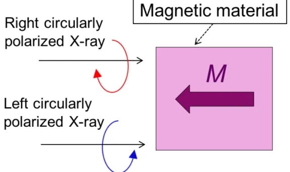
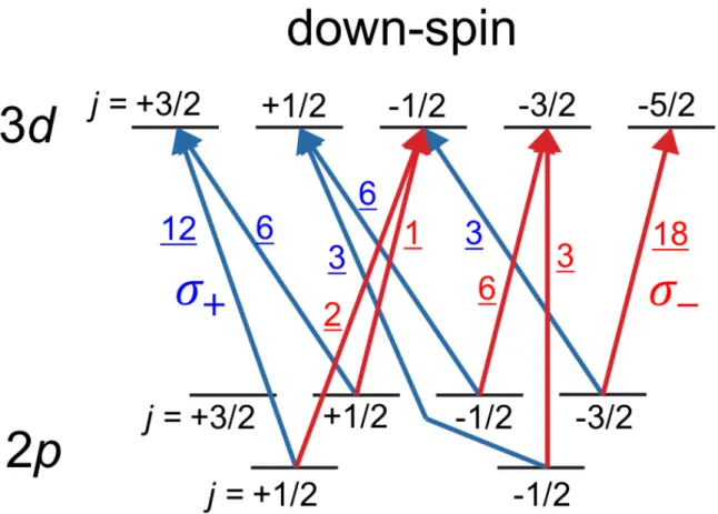
In XMCD measurements,24 we measure the difference of the absorption between right- and left- circularly polarized X-ray (Fig. 3). Figure 4 shows a schematic diagram of the relative transition probabilities between the 2p core levels and the 3d down-spin states of Fe. Here, relative transition probabilities between the 2p core levels and the 3d up-spin states of Fe are not shown for simplicity, because most of the 3d up-spin states are occupied in Fe atoms. The degeneracy of the 2p core levels is resolved by the spin-orbit interactions, which results in the two-fold degenerated 2p1/2 and the four-fold degenerated 2p3/2 levels. The
magnetic moment of Fe reflects the difference of the occupancies between the up-spin states and down-spin states of the 3d levels. In XMCD, this difference of the occupancy is detected as the difference of the absorption between the right- and left- circularly polarized X-rays. XMCD has following large advantages. First, we can detect element-specific magnetic moments using 2p-3d absorption edges which depend on elements. Second, we can separately estimate orbital and spin magnetic moments using the XMCD sum rules. In addition, the sum of the absorptions is called X-ray absorption spectroscopy (XAS). Using XAS, we can estimate a valence of atoms.
Fig. 4. Schematic diagram of the relative transition probabilities between the 2p core levels and the 3d
down-spin states of Fe.
See the section 3.3 and 5.3 for detailed explanations of the XMCD sum rules and examples of its application.
2. 2. Angle resolved photoemission spectroscopy (ARPES)
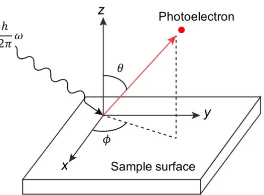
Angle resolved photoemission spectroscopy (ARPES) is a powerful technique to observe the electronic structure of solids using the photoelectric effect.25,26 Figure 5 shows the experimental configuration of the ARPES measurements. In the ARPES measurements, we detect numbers, kinetic energies, and the directions of the photoelectrons escaping from the sample surface when the X-ray is irradiated to the sample surface. In the ARPES measurements, we can observe the density of states and the band dispersion.
Fig. 5. Experimental configuration of the ARPES measurements. The red arrow represents the direction of the
photoelectron escaped from the sample surface. The angle 𝜃 represents the polar angle between the normal line
of the sample surface and the the direction of the photoelectron. The angle 𝜙 represents the azimuthal angle in
the sample surface.
Fig. 6. Schematic illustration of the energy conservation in ARPES.
ℎ
2#
$
z
x
y
%
&
Sample surface
Photoelectron
ℎ
2#
$
Ener gy Wave vectorFree electron band
band in the sample
Sample surface Sample Vacuum Ei Ef E0 W EK Fermi level (EF= 0) (defined as the energy origin) Vacuum level Photoelectron
Figure 6 shows the schematic illustration of the energy conservation in ARPES. The principle of ARPES can be explained in accordance with Fig. 6.
The electron on the energy band in the sample is excited to the final state, whose energy is Ef, from the initial state, whose energy is Ei, by irradiating the X-ray with the photon energy of (h/2𝜋)𝜔. In this process, the following energy conservation is kept.
'(& 𝜔 = 𝐸𝑓 − 𝐸𝑖. (1) We can view the electron at the final state to be a free electron. Here, E0 is defined as the
energy difference between the Fermi level (EF) and the bottom of the energy band of the free
electron. Here, EF is defined as the energy origin. Thus, Ef is expressed as follows. 𝐸/= ℏ
2(𝑘
∥2 + 𝑘⊥2)
2𝑚 − 𝐸9, (2)
where, 𝑘: and 𝑘∥ represent the perpendicular and in-plane components of the wave number
of the electron at the final state.
In addition, the following energy conservation between the electron at the final state and the photoelectron escaped from the surface is kept.
𝐸/ = 𝐸;+ 𝑊, (3) where, EK and W represent the kinetic energy of the photoelectron escaped from the surface
and the work function of the sample, respectively.
The perpendicular (𝐾:) and in-plane (𝐾∥) components of the wave number of the
photoelectron escaped from the surface are expressed as follows. 𝐾:=
2𝑚𝐸K
ℏ cos 𝜃, (4)
𝐾∥= 2𝑚𝐸ℏ Ksin 𝜃, (5) where, 𝜃 represents the polar angle shown in Fig. 5.
When the sample surface is flat, the in-plane component of the wave number does not change, e.g.
𝐾∥= 𝑘∥, (6) By solving eqs. (1)-(6), we can obtain the following equations.
𝑘: =
2𝑚{𝐸𝑖 + ℏ𝜔 − 𝑊}cos2𝜃 + 𝐸
0 + 𝑊
ℏ . (8)
In addition, x and y components of the wave number of the electron at the final state are expressed as follow.
𝑘G = 𝑘∥cos 𝜙, (9)
𝑘H = 𝑘∥sin 𝜙, (10) In the ARPES measurements, we observe 𝜃, 𝜙, and 𝐸;. In addition, we obtain the W value by reference measurements typically for Au electrically contacting the sample. Thus, by using eqs. (1) and (3), we can obtain 𝐸I. In addition, by using eqs. (7)-(10), we can determine the band dispersion of the sample. The 𝐸9 value is treated as a fitting parameter in the ARPES measurements. In this thesis, the energy resolution of the ARPES measurements is estimated to be 170 meV. Note that the accuracy of the energy position of the EF is much
higher (typically ~10 meV). This can be determined by the shape of the photoemission spectrum near EF for Au.27
2. 3. Tunneling magnetoresistance (TMR)
MTJs are tunnel junctions composed of two FM electrodes and a insulating tunnel barrier.28 TMR occurs in MTJs. The directions of the magnetizations of the two FM electrodes can be controlled separately by an external magnetic field or a spin transfer torque. When the magnetizations are aligned parallel, the tunneling probability of the electrons is higher than that when the magnetizations are aligned antiparallel. Therefore, MTJs can be switched between high and low resistance states. The TMR is applied to the magnetic head of the HDD and the magnetoresistive random access memory (MRAM). Observation of the TMR in MTJ is direct evidence of a finite spin polarization of the FM electrodes because the TMR originates from the spin polarization of the FM electrodes as explained below.
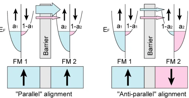
Fig. 7. Schematic illustration of the spin-dependent tunneling process at the parallel alignment and antiparallel
alignment of the two FM electrodes in the MTJ, where carriers tunnel from FM1 electorde to FM2 electrode
through the tunnel barrier, and a1 and a2 represent the existence probability of the majority spin at the EF for the
FM1 and FM2, respectively.
Assuming that carriers tunnel without spin flip, up-spin carriers of one FM layer are allowed to tunnel only into the up-spin state of the other FM layer, and down-spin carriers are allowed to tunnel only into the down-spin state of the other FM layer. The tunneling probability of the up-spin (down-spin) carriers depends on the density of states (DOS) of the up-spin (down-spin) band of both FM layers. Figure 7 shows the schematic illustrations of the spin-dependent tunneling process in the parallel magnetization alignment and antiparallel magnetization alignment of the two FM electrodes in the MTJ, where carriers tunnel from FM1 electorde to FM2 electrode through the tunnel barrier, and a1 and a2 represent the ratio
of the density of the majority spin at the EF to that of the sum of the majority and minority
spins for FM1 and FM2, respectively. The tunnel conductances of carriers in parallel magnetization (GP) and anti-parallel magnetization (GAP) are described as follows.
𝐺P ∝ 𝑎O𝑎'+ (1 − 𝑎O)(1 − 𝑎'). (11)
𝐺AP ∝ 𝑎O(1 − 𝑎') + (1 − 𝑎O)𝑎'. (12) Using the resistance in the parallel magnetization (RP) and the one of anti-parallel
magnetization (RAP), the TMR ratio is given by the following equation,
𝑇𝑀𝑅 = 𝑅AP𝑅 − 𝑅P
P =
𝐺P − 𝐺AP
where R = 1/G is used. Defining the spin polarization P as P1, 2 = a1, 2 - (1 - a1, 2) = 2a1, 2 - 1,
Eq. (13) is transformed as,
𝑇𝑀𝑅 = 1−𝑃2𝑃1𝑃2
1𝑃2. (14)
Eq. (14) means that the FM electrodes with a high spin polarization will give a high TMR ratio.
Chapter 3: Crystal Structure, Annealing Effect, Magnetic
Properties, and Electronic Structure of the
Ferromagnetic Semiconductor Ge
1-xFe
x3. 1. Crystal structure and magnetic properties
In this section, we present the growth temperature (TS) dependence of TC, the lattice
constant, the non-uniformity of Fe atoms, and the stacking-fault defects of GeFe films, that are investigated by magnetic circular dichroism (MCD), X-ray diffraction (XRD), high-resolution transmission electron microscopy (HRTEM), and spatially resolved transmission electron diffraction (TED) combined with energy dispersive X-ray spectroscopy (EDX). Also, we employ channeling Rutherford backscattering (c-RBS) and channeling particle induced X-ray emission (c-PIXE) characterizations to investigate the location of the Fe atoms in the GeFe lattice.29
We have epitaxially grown Ge1-xFex thin films with the Fe concentration x of 0.065 and 0.105 on Ge(001) substrates by LT-MBE. Figure 8(a) shows the schematic structure of the samples. The growth process is described as follows. After the Ge(001) substrate was chemically cleaned and its surface was hydrogen-terminated by buffered HF solution, it was introduced in the MBE growth chamber through an oil-free load-lock system. After degassing the substrate at 400°C for 30 minutes and successive thermal cleaning at 900ºC for 15 min, we grew a 30-nm-thick Ge buffer layer at 200ºC, which was followed by the growth of a 120-nm-thick Ge0.935Fe0.065 layer at TS = 160-280ºC (8 samples) or a 120-nm-thick
Ge0.895Fe0.105 layer at TS = 200-280ºC (6 samples). After that, we grew a 2-nm-thick Ge
capping layer at 200ºC to avoid the surface oxidation of the GeFe layer. We used in-situ reflection high-energy electron diffraction (RHEED) to monitor the crystallinity and surface morphology of the Ge buffer layer, GeFe layer, and Ge capping layer during the growth. Figure 8(b)-(d) shows the RHEED patterns of (b) the Ge buffer layer surface, (c) 120-nm-thick Ge0.935Fe0.065 layer surface grown at TS = 240°C, and (d) 2-nm-thick Ge
capping layer surface with the electron-beam azimuth along the <110> direction of the Ge(001) substrate. The diffraction pattern of the Ge buffer layer surface showed intense and sharp 2 × 2 streaks, which indicate a 2-dimensional growth mode and exhibit a diamond-type single crystal structure, and also the weak Kikuchi lines indicating good crystallinity. The GeFe layer surface showed intense and sharp 2 × 2 streaks but with no clear Kikuchi lines. The Kikuchi lines appeared again after the growth of the Ge capping layer.
Fig. 8. (a) Schematic structure of the samples consisting of Ge cap (2 nm) / Ge1-xFex (120 nm) / Ge buffer (30
nm) / Ge(001) substrate. (b)-(d) RHEED patterns of (b) the Ge buffer layer surface, (c) 120-nm-thick Ge0.935Fe0.065 layer surface grown at TS = 240°C, and (d) 2-nm-thick Ge capping layer surface with the
electron-beam azimuth along the <110> direction of the Ge (001) substrate. [Y. K. Wakabayashi et al., Journal of Applied Physics 116, 173906 (2014).]
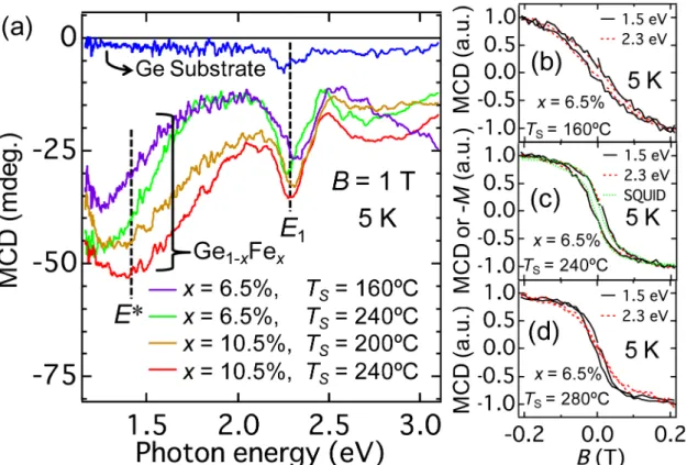
Fig. 9. (a) MCD spectra of the Ge substrate (blue curve), of the Ge0.935Fe0.065 (x = 0.065) films grown at TS
= 160ºC (violet curve) and TS = 240ºC (green curve), and of the Ge0.895Fe0.105 (x = 0.105) films grown at TS
= 200ºC (brown curve) and TS = 240ºC (red curve), with a magnetic field B of 1 T applied perpendicular to
the film plane at 5 K. (b)-(d) MCD intensity as a function of B measured at 5 K with the photon energies of 1.5 eV (black curve) and 2.3 eV (red dotted curve) for the Ge0.935Fe0.065 films grown at (b) TS = 160ºC, (c)
TS = 240ºC, and (d) TS = 280ºC. In (c), the green dotted curve expresses the B dependence of −M
measured by SQUID. [Y. K. Wakabayashi et al., Journal of Applied Physics 116, 173906 (2014).]
We have carried out magneto-optical measurements on the GeFe films to investigate the
TS dependence of TC. MCD, which is defined as the difference between the optical
reflectances of right- and left- circular polarized lights, is a powerful tool to investigate the magnetic properties of FMSs.30 This is because the MCD intensity is proportional to the
s,p-d exchange interaction, which is considered to be the origin of the ferromagnetism in
FMSs, and also proportional to the vertical component of the magnetization (M) in FMSs. Figure 9(a) shows the MCD spectra of the Ge substrate (blue curve), of the Ge0.935Fe0.065
films grown at TS = 160ºC (violet curve) and 240ºC (green curve), and of the Ge0.895Fe0.105
films grown at TS = 200ºC (brown curve) and 240ºC (red curve), with the magnetic field B of
1 T applied perpendicular to the film plane at 5 K. All the GeFe samples show the E1 peak at
around 2.3 eV corresponding to the L point of the bulk Ge as we can see in the MCD spectrum of the Ge substrate. These E1 peaks, that are enhanced by the s,p-d exchange
interaction in all the GeFe films, are the characteristic property of FMSs.31 The broad peak (E*) at around 1.4 eV observed in all the GeFe samples is thought to be related to the Fe-related impurity bands or d-d transitions.32 Figure 9(b)–(d) shows the B dependence of the MCD intensities measured at 5 K with the incident photon energies of E* (1.5 eV, black curve) and E1 (2.3 eV, red dotted curve) for the Ge0.935Fe0.065 films grown at (b) 160ºC, (c)
240ºC, and (d) 280ºC. Figure 9(c) also shows the B dependence of the normalized −M (green dotted curve) measured by a superconducting quantum interference device (SQUID). Here, the diamagnetic signal of the Ge substrate was subtracted from the raw M data. As shown in Fig. 9(b) and (c), in the Ge0.935Fe0.065 films grown at 160ºC and 240ºC, the shapes of
the MCD - B curves at 1.5 eV and 2.3 eV are identical with each other, which means that the MCD signals at 1.5 eV and 2.3 eV originate from the same FM phase of GeFe.33 Moreover, Fig. 9(c) shows that the shapes of the MCD - B curves are the same as that of the −M vs. B curve measured by SQUID. This indicates that the M data measured by SQUID has the same origin as that induces the spin splitting of the energy band of GeFe. These results indicate that the origin of the ferromagnetism is the single FMS phase of GeFe. In the Ge0.935Fe0.065 film
grown at 280ºC, the shapes of the MCD - B curves at 1.5 eV and 2.3 eV are not identical with each other [Fig. 9(d)], indicating that there are two or more magnetic phases in the film. From the same analyses on other samples, we have found that the Ge1-xFex films grown with the range of TS from 160ºC to 260ºC have a single FMS phase for both of x = 0.065 and 0.105.
Figure 10(a) shows the B dependence of the MCD intensity of the Ge0.935Fe0.065 film
grown at TS = 240°C measured with the incident photon energy of 2.3 eV at 5 K (blue curve),
80 K (violet curve), 100 K (orange curve), and 110 K (red curve). In the inset of the close-up view near zero magnetic field, a clear hysteresis curve is observed up to 100 K. In Fig. 10(b), we have estimated TC using the Arrott plots (MCD2 - B/MCD) of the MCD-B curves
measured with the incident photon energy of 2.3 eV at various temperatures for the Ge0.935Fe0.065 film grown at TS = 240°C. In the plots, we can estimate the square of the
spontaneous MCD (∝ M) by extrapolating the data in the high magnetic-field region (0.8-1.25 T), where the MCD2 - B/MCD data is sufficiently linear for accurately estimating
TC. This method is well-established and convenient because it is free from the effect of the
magnetic anisotropy which affects the low-magnetic-field properties and sometimes makes the accurate estimation of TC difficult. The estimated TC is 100 K in this film, and we can see
that the same TC value is obtained both from the hysteresis loop analysis shown in the inset of
Fig. 10(a) and from the Arrott plots in Fig. 10(b).
In Fig. 10(a), the MCD-B curve at 110 K, that is above TC (= 100 K), still has a large
curvature, indicating that superparamagnetism appears above TC. Because any second-phase
or in the MCD analyses in our GeFe films, this origin is not the FM intermetallic Fe-Ge precipitates. Meanwhile, because we see non-uniform distribution of the Fe atoms in these HRTEM lattice images of our films, the large curvature of the MCD - B curve indicates that the local FM regions are formed only in the high-Fe-concentration regions by the short-range interaction even above TC. The similar local FM regions have been observed in III-V-based
FMS (Ga,Mn)As34 and II-VI-based FMS (Zn,Cr)Te.35
Fig. 10. (a) MCD intensity as a function of B of the Ge0.935Fe0.065 film grown at TS = 240°C measured with the
incident photon energy of 2.3 eV at 5 K (blue curve), 80 K (violet curve), 100 K (orange curve), and 110 K (red curve). The inset shows the close-up view near zero magnetic field. (b) Arrott plots of the MCD-B data
measured with the incident photon energy of 2.3 eV at various temperatures for the Ge0.935Fe0.065 film grown at
TS = 240°C. [Y. K. Wakabayashi et al., Journal of Applied Physics 116, 173906 (2014).]
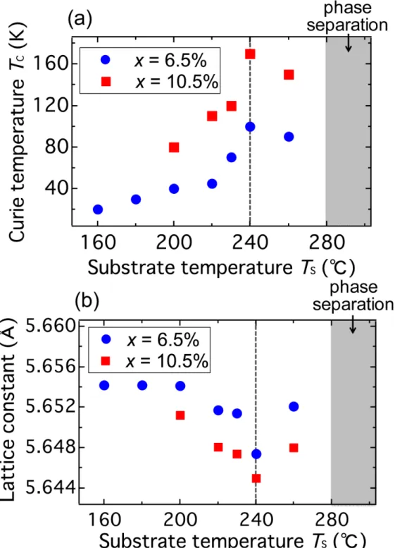
Figure 11(a) shows the TS dependence of TC of the Ge0.935Fe0.065 (x=0.065) films grown
at TS = 160-260ºC (blue circles) and the Ge0.895Fe0.105 (x=0.105) films grown at TS =
200-260ºC (red squares). When TS ≥ 280ºC (gray area), the GeFe films were phase-separated
magnetically as mentioned above. Here, we estimated the TC values using the Arrott plots of
MCD at 2.3 eV. For both of x, the maximum TC is achieved when TS = 240ºC. The saturation
magnetization MS, that was obtained at 5 K by SQUID with a magnetic field of 1 T applied
perpendicular to the film plane, in the Ge0.935Fe0.065 films grown at TS = 160ºC (TC = 20 K)
and TS = 240ºC (TC = 100 K) is 0.7µB and 1.3µB per one Fe atom, respectively, where µB is
the Bohr magneton. The MS in the Ge0.895Fe0.105 films grown at TS = 200ºC (TC = 80 K) and TS = 240ºC (TC = 170 K) is 0.7 µB and 1.0 µB per one Fe atom, respectively. For both x, the
magnetic moment increases with increasing TC, which suggests that MS is related to the
Fig. 11. (a) Curie temperature TC as a function of TS of the Ge0.935Fe0.065 films (blue circles) and Ge0.895Fe0.105
films (red squares), that were estimated by the Arrott plots (MCD2 - B/MCD) with the photon energy of 2.3 eV,
where B is the magnetic field. (b) Lattice constant as a function of TS of the Ge0.935Fe0.065 (x=0.065) films grown
at TS = 160-260ºC (blue circles) and the Ge0.895Fe0.105 (x=0.105) films grown at TS = 200-260ºC (red squares). [Y.
Fig. 12. (a),(b) HRTEM lattice images of the Ge0.935Fe0.065 layer grown at (a) TS = 160ºC and (b) TS = 240ºC
projected along the Ge[110] axis. (c)-(f) TED images taken at (c) the point *1 (bright region), (d) the point *2
(dark region) in the Ge0.935Fe0.065 layer grown at TS = 160ºC, (e) the point *3 (bright region), and (f) the point *4
(dark region) in the Ge0.935Fe0.065 layer grown at TS = 240ºC. [Y. K. Wakabayashi et al., Journal of Applied
Physics 116, 173906 (2014).]
Figure 12 shows the HRTEM lattice images of the Ge0.935Fe0.065 films grown at (a) TS =
160ºC and (b) TS = 240ºC projected along the Ge[110] axis. The both images indicate that the
Ge0.935Fe0.065 layers have a diamond-type single-crystal structure. Although there is color
(bright and dark) shading which is attributed to the non-uniform distribution of Fe atoms both in (a) and (b), there are no other ferromagnetic intermetallic Fe-Ge precipitates with a
different crystal structure. By the spatially resolved EDX measurements, the local Fe concentration at *1 (bright region) and *2 (dark region) in the Ge0.935Fe0.065 film grown at TS
= 160ºC shown in Fig. 12(a) was estimated to be 4±1% and 7±1%, respectively. The local Fe concentration at *3 (bright region) and *4 (dark region) in the Ge0.935Fe0.065 film grown at TS
= 240ºC shown in Fig. 12(b) was estimated to be 3±1% and 10±1%, respectively. These results mean that the non-uniformity of Fe atoms in the Ge0.935Fe0.065 film grown at TS =
240ºC is larger than that in the Ge0.935Fe0.065 film grown at TS = 160ºC. Figure 12(c)-(f) shows
the TED images at *1-*4. The TED images at point *1 (bright region), *2 (dark region) in the Ge0.935Fe0.065 film grown at TS = 160ºC, and *3(bright region) in the Ge0.935Fe0.065 film grown
at TS = 240ºC showed the diffraction patterns of the diamond structure without any other
crystal phases. The TED image at point *4 (dark region) in the Ge0.935Fe0.065 film grown at TS
= 240ºC showed the diffraction pattern of the diamond structure with weak extra spots caused by stacking-fault defects along the (111) plane, which indicates that the density of the stacking-fault defects in the Ge0.935Fe0.065 film grown at TS = 240ºC is larger than that in the
Ge0.935Fe0.065 film grown at TS = 160ºC.
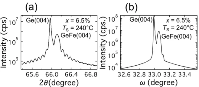
Fig. 13. (a),(b) XRD (a) θ-2θ spectrum and (b) rocking curve of the GeFe(004) reflection of the Ge0.935Fe0.065
film grown at TS = 240ºC. [Y. K. Wakabayashi et al., Journal of Applied Physics 116, 173906 (2014).]
Figure 13 shows (a) the XRD θ-2θ spectrum and (b) the XRD rocking curve of the GeFe(004) reflection of the Ge0.935Fe0.065 film grown at TS = 240ºC. In Fig. 13(a), the (004)
diffraction peak of the GeFe film is clearly seen on the higher-angle side of the Ge(004) peak with the clear fringes, which indicates that the film is a high-quality single crystal with an abrupt and smooth interface. The excellent crystallinity of the Ge0.935Fe0.065 film grown at TS
= 240ºC is also confirmed by the XRD rocking curve of the GeFe(004) reflection shown in Fig. 13(b) exhibiting a narrow full width at half maximum of 0.03º, which is comparable to
that of the Ge substrate, 0.01º.36-38 Figure 11(b) shows the TS dependence of the lattice
constant that is estimated from the XRD spectra of the Ge0.935Fe0.065 (x=0.065) films grown at TS = 160-260ºC (blue circles) and the Ge0.895Fe0.105 (x=0.105) films grown at TS = 200-260ºC
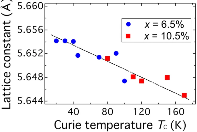
(red squares). For both of x, the lattice constant is minimum at TS = 240ºC. Figure 14 shows
the lattice constant of the Ge0.935Fe0.065 films grown at TS = 160-260ºC (blue circles) and the
Ge0.895Fe0.105 films grown at TS = 200-260ºC (red squares), plotted as a function of TC. We see
a universal relationship between the TC and the lattice constant, which does not depend on x.
The TC value increases as the lattice constant of the GeFe films decreases.
Fig. 14. Lattice constant estimated from the XRD spectra plotted as a function of TC of the Ge0.935Fe0.065 films
(blue circles) and the Ge0.895Fe0.105 films (red squares). [Y. K. Wakabayashi et al., Journal of Applied Physics
116, 173906 (2014).]
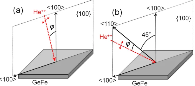
We employed c-RBS and c-PIXE to determine the position of the Fe atoms in the host Ge lattice. Figure 15 shows our experimental configurations of the PIXE-Fe- Kα and the RBS angular scans in the {100} plane (a) around the <100> axis and (b) around the <110> axis. The red dotted arrows represent the direction of the incident 4He++ beam. We measured the scattering yields as a function of the incident angle φ, that is defined as the angle between the crystal-axial (<100> or <110>) direction and the incident direction of an energetic ion beam
of 4He++, by varying φ in a few degrees from 0º. Ideally, the scattering yields have a minimum value at φ=0º, where the incident beam is perfectly aligned in the crystal axis and the scattering is most suppressed, while they tend to increase and finally saturate when |φ| becomes larger than several degrees.39 - 42 We define 𝜒𝒅(𝐴) as the scattering yield
originating from the element A normalized by the averaged value of the scattering yields at |φ| ranging from 2.5 to 3º when the measurement is carried out around the d crystal-axial direction. Also, 𝜒YZ[𝒅 (𝐴) is defined as the minimum value of 𝜒𝒅(𝐴), that is obtained at φ=0º.
Figure 16(a) shows the schematic illustration of the possible sites that can be occupied in the diamond-type lattice structure, including the substitutional (or host) sites S (yellow spheres), the bond-center site BC (black sphere), the antibonding sites Q (violet spheres), the hexagonal site H (blue sphere), and the tetrahedral sites T (red spheres).43,44 Here, we refer to these sites as specific sites. Figure 16(b),(c) illustrates the locations of these specific sites when seen from the <100> and <110> directions, respectively. We note that other sites that are equivalent to these specific sites are neglected in Fig. 16 for simplicity.
Fig. 15. (a),(b) Experimental configurations of the PIXE-Fe-Kα and RBS angular scans in the {100} plane (a)
around the <100> axis and (b) around the <110> axis. The red dotted arrows represent the direction of the
incident 4He++ beam, and φ represents the angle between the incident beam direction and the axial direction. [Y.
Fig. 16. (a) Schematic illustration of the possible specific sites in the diamond-type lattice structure, including
the substitutional sites S (yellow spheres), the bond-center site BC (black sphere), the antibonding sites Q (violet spheres), the hexagonal site H (blue sphere), and the tetrahedral sites T (red spheres). (b),(c) The location of the specific sites when seen from the (b) <100> and (c) <110> directions. [Y. K. Wakabayashi et al., Journal of Applied Physics 116, 173906 (2014).]
Figure 17(a)-(d) shows the PIXE-Fe-Kα and RBS angular scans in the {100} plane (a),(c) around the <100> axis and (b),(d) around the <110> axis for the Ge0.935Fe0.065 films
grown at (a),(b) TS = 160ºC and (c),(d) TS = 240ºC measured with a 2.275-MeV-4He++ beam.
In all the graphs, the normalized yield has a minimum value at φ ≈ 0º, which indicates that a lot of Fe atoms are shadowed by the host atoms and that they are not visible to the beam along the <100> or <110> axial directions. Ideally, 𝜒YZ[\O99](Ge) and 𝜒
YZ[\OO9](Ge) should be
nearly zero.43 In our case, however, 𝜒YZ[\O99](Ge) (=0.25 and 0.32 in the Ge
0.935Fe0.065 films
grown at TS = 160ºC and 240ºC, respectively) and 𝜒YZ[\OO9](Ge) (=0.12 and 0.10 in the
Ge0.935Fe0.065 films grown at TS = 160ºC and 240ºC, respectively) are larger than zero. We
think that these results are attributed to the local fluctuation of the host Ge atom positions (lattice fluctuation) in our GeFe films, which is probably caused by the stacking-fault defects and the non-uniform Fe distribution. However, we obtained nearly the same values of
𝜒YZ[\O99](Ge) (=0.25 and 0.32) and 𝜒
YZ[\OO9](Ge) (=0.12 and 0.10) in the both samples grown at
different TS, which means that this local lattice fluctuation is not sensitive to TS. Because we
discuss the TS dependence of the Fe location here, the lattice fluctuation is not so important
for this purpose as long as the yield does not depend on TS. Thus, we neglect the influence of
Fig. 17. (a)-(d) PIXE-Fe-Kα (solid red circles) and RBS (blank red squares) angular scans around (a),(c) the
<100> axis and (b),(d) the <110> axis for the Ge0.935Fe0.065 films grown at (a),(b) TS = 160ºC and (c),(d) TS =
240ºC. [Y. K. Wakabayashi et al., Journal of Applied Physics 116, 173906 (2014).]
The first important point is that 𝜒YZ[\O99](Fe) is almost the same as 𝜒
YZ[\O99](Ge) in both
samples [Figs. 17(a) and 17(c)]. This result indicates that most Fe atoms are located on the S or T sites because the specific sites which are shadowed by the host atoms in the <100> axial direction are only the S and T sites as we can see in Fig. 16(b). We define fS+T as the sum of
the densities of the Fe atoms located on the S and T sites divided by the total density of the Fe atoms. We can estimate fS+T by using the following equation with 𝜒YZ[\O99](Fe) and
𝜒YZ[\O99](Ge) obtained in the <100> axial direction:39
𝑓S+T = 1 − 𝜒YZ[\O99] Fe / 1 − 𝜒YZ[\O99] Ge . (15)
By using eq. (15), fS+T in the Ge0.935Fe0.065 films grown at TS = 160ºC and TS = 240ºC is
grown at TS = 160ºC and TS = 240ºC, the small fraction of 7% and 4% of the doped Fe atoms
is located on the sites other than the S or T sites.
The second important point is that 𝜒YZ[\OO9](Fe) is higher than 𝜒
YZ[\OO9](Ge) in the both
Ge0.935Fe0.065 films grown at TS = 160ºC [Fig. 17(b)] and TS = 240ºC [Fig. 17(d)]. As can be
seen in Figs. 16(b) and 16(c), the Fe atoms on the T sites in the diamond lattice are shadowed by the host atoms in the <100> direction but are exposed in the <110> direction. The atoms on the T sites are irradiated by the beam in all the φ range shown in Fig. 17(b) and 17(d). It is known that the yields coming from the exposed atoms on the T sites are slightly enhanced in the vicinity of the <110> direction (φ ≈ 0º) due to the flux peaking effect,45 which has been well understood both theoretically46 and experimentally.47 The flux peaking effect is induced by the increase in the flux of the incident energetic ion beam near the T sites in the <110> direction.48-50 From the numerical calculation, the enhancement factor F for a surface layer, which is defined as the ratio of the intensity of the Fe-Kα-X-rays coming from the atoms on the T sites at φ=0º to that at |φ|=2º, has been estimated to be in the range of 1.8 - 2.2 in the <110> axis for a diamond cubic lattice.39,43 The ratio fT of the density of the Fe atoms on the
T sites to the sum of those on the S and T sites can be obtained from the <110> channeling results by the following equation:49
𝜒YZ[\OO9] Fe = 1 − 𝑓
S+T + 𝑓S+T 𝐹𝑓T+ 𝜒YZ[\OO9] Ge 1 − 𝑓T . (16)
By eq. (16), fT in the Ge0.935Fe0.065 films grown at TS = 160ºC and TS = 240ºC is estimated to
be 13-16% and 15-18%, respectively. In the case of typical III-V-based FMS (Ga,Mn)As, the similar fractions of the Mn atoms on the T sites have been found,50 ,51 and it has been known
that the density of the substitutional Mn atoms is correlated with TC, which means that they
determine the FM properties of (Ga,Mn)As films.34,52 In the case of GeFe, however, we do
not see a clear difference in the Fe density on the T sites between the two samples, which have the large difference in the TC values (20 K and 100 K for the films grown at TS = 160ºC
and TS = 240ºC, respectively). This indicates that the ferromagnetism in GeFe is not directly
related to the density of the substitutional Fe atoms.
As described above, the fT values obtained in the Ge0.935Fe0.065 films grown at TS =
160ºC (TC = 20 K, MS = 0.7 µB per one Fe atom) and TS = 240ºC (TC = 100 K, MS = 1.0 µB
per one Fe atom) are almost the same (13-16% and 15-18%, respectively), but the lattice constants (5.654 and 5.647 Å), Fe concentration fluctuations (4-7% and 3-10%), and the stacking-fault densities are different between them. Our results indicate that these characteristics, except for fT, are correlated with the ferromagnetism. Similar crystallographic
changes have been reported in face-centered cubic crystals (CuMnSi and CrMnNi alloys), in which the (004) diffraction peak shifts to the higher angle side with an increase in the density of the stacking-fault defects along the (111) plane.53-55 Our results mean that the non-uniform
distribution of the Fe atoms is a key factor in determining the detailed crystallographic features and magnetic properties.56 The same tendency has been observed in the annealing-temperature dependence of the GeFe films (see section 3.2).32 When the non-uniformity of the Fe concentration is enhanced, the locally high-Fe-concentration regions can easily connect each other magnetically, resulting in higher TC. In III-V and II-VI-based
FMSs, such an increase in TC due to the enhancement of the non-uniformity of the magnetic
impurities is predicted theoretically57 by the random phase approximation in the Heisenberg model.58,59 Thus, room-temperature ferromagnetism will be achieved by doping a higher concentration of Fe atoms and enhancing the non-uniformity of Fe atoms adequately. The important point is that the GeFe films have a single FMS phase which is confirmed by the MCD and SQUID measurements [see Fig. 9(c)], even though they have the non-uniformity of the Fe concentration. This means that, once ferromagnetism appears, the locally high-Fe-concentration regions and low-Fe-concentration regions are magnetically coupled by the s,p-d exchange interaction, which is confirmed by the enhancement of the E1 peak in the
MCD spectra [see Fig. 9(a)].
In summary of this section, we have studied the TS dependence of TC, the lattice constant,
the non-uniformity of Fe atoms, and the stacking-fault defects of the Ge1-xFex films with x = 0.065 and 0.105, and observed continuous changes in TC and in the lattice constant as a
function of TS. The TC value increases with the decrease in the lattice constant, and the
relationship between TC and the lattice constant does not depend on x. The TC reaches
maximum values of 100 K and 170 K when TS = 240ºC for x = 0.065 and 0.105, respectively.
By using the spatially resolved TED combined with the EDX, we have found that the density of the stacking-fault defects and the non-uniformity of Fe atoms in the Ge0.935Fe0.065 film
grown at TS = 240ºC are larger than those in the Ge0.935Fe0.065 film grown at TS = 160ºC. By
using c-RBS and c-PIXE characterizations, we have found that the small fraction of 7% and 4% of the doped Fe atoms are located on the sites other than the S or T sites in the Ge0.935Fe0.065 samples with TC of 20 and 100 K, respectively. Among the Fe atoms located on
the S and T sites, 13-16% and 15-18% of them exist on the T sites in the Ge0.935Fe0.065 films
with the different TC values of 20 and 100 K, respectively. By considering these results, we
conclude that the non-uniformity of the Fe concentration and the stacking-fault defects formed in the high Fe concentration region play an important role in determining the FM properties of the GeFe films. The influences of the tetrahedral interstitial magnetic impurities on the ferromagnetic properties are completely different between GeFe and (Ga,Mn)As.
3. 2. Annealing effect
The current problem of GeFe is its low TC, which is at the highest 170 K as shown in Fig.
11. Recently, GeFe quantum dots with a high TC of ~400 K without any observable
precipitates have been reported.60 Thus, if we can grow GeFe quantum dots (or nano-particles) inside a Ge film with a flat surface or interfaces with other layers (or substrates), they are very promising. In fact, the ferromagnetic MnAs nano-particles embedded in GaAs have shown intriguing properties induced by Coulomb blockade and spin-dependent tunneling.61,62 In III-V-based FMS (Ga,Mn)As, post-growth annealing is known to be a powerful technique to improve the TC by removing the interstitial Mn atoms
from the (Ga,Mn)As layer.63,64 In this section, we investigate the annealing effect on GeFe in order to enhance the ferromagnetism of GeFe and its relevance to the structural and magnetic properties. Through this study, we find that the ferromagnetism of GeFe becomes strong with the enhancement of the non-uniformity of the Fe atoms by the annealing.
The Ge0.895Fe0.105 thin film studied here was epitaxially grown on a Ge(001) substrate by
LT-MBE. The growth process is described as follows. After the Ge(001) substrate was chemically cleaned and its surface was hydrogen-terminated by buffered HF solution, it was introduced in the MBE growth chamber through an oil-free load-lock system. After degassing the substrate at 400°C for 30 min and successive thermal cleaning at 900°C for 15 min, a 30-nm-thick Ge buffer layer was grown at 200°C, followed by the growth of a 60-nm-thick Ge0.895Fe0.105 layer at 240°C. The in-situ RHEED was used to observe the crystallinity and
morphology of the surface during the growth. The diffraction pattern of the Ge buffer layer surface showed intense and sharp 2 × 2 streaks, and the Ge0.895Fe0.105 surface also showed a 2
× 2 pattern with no extra spots, indicating two-dimensional epitaxial growth. Post-growth annealing was carried out in a nitrogen atmosphere for 30 min at 400, 500, and 600°C.
The crystallographic analyses of the Ge0.895Fe0.105 films were performed by HRTEM.
Figure 18(a),(b) shows the HRTEM lattice images of the Ge0.895Fe0.105 film as grown and
annealed at 500°C projected along the Ge [110] axis, respectively. The both images indicate that the Ge0.895Fe0.105 layers have a diamond-type single-crystal structure with an atomically
flat surface. Although the color (dark and bright) contrast in the GeFe layer is attributed to the non-uniform distribution of Fe atoms and stacking-fault defects as discussed in section 3.1, there are no other ferromagnetic intermetallic Fe-Ge precipitates with a different crystal structure.
Fig. 18. (a)-(c) HRTEM lattice images projected along the Ge[110] axis of Ge0.895Fe0.105 (a) as grown and after
annealing at (b) 500°C and (c) 600°C. [Y. K. Wakabayashi et al., Physical Review B 90, 205209 (2014).]
Fig. 19. (a) HRTEM lattice image projected along the Ge[110] axis of a ferromagnetic nano-particle formed in
the Ge0.895Fe0.105 film after annealing at 600°C. (b),(c) TED images obtained from (b) the
diamond-crystal-structure region (*1) and from (c) the nano-particle (*2). [Y. K. Wakabayashi et al., Physical Review B 90, 205209 (2014).]
Figure 18 (c) shows a HRTEM lattice image of the Ge0.895Fe0.105 film annealed at 600°C
projected along the Ge [110] axis, where we see many nano-particles formed in the film. Figure 19 (a) shows the magnified view of the HRTEM lattice image of one of the nano-particles in the Ge0.895Fe0.105 film annealed at 600°C, indicating that the nano-particles
have periodic twins and stacking faults. By the spatially resolved TED combined with the spatially resolved EDX, the local electron-diffraction pattern and Fe concentration were obtained. In the EDX measurements, the error bar of the Fe concentration is ±1%, which mainly originates from the sample drift of ~1 nm during the measurements. The local Fe concentration at *1 (bright region) and *2 (dark region) of the GeFe film annealed at 500°C shown in Fig. 18 (b) was estimated to be 8 and 23%, respectively. When the annealing temperature is 600°C, the local Fe concentration at *1 (homogeneous diamond-crystal-structure region) and *2 (inside the nano-particle) in Fig. 19 (a) was estimated to be 5 and 25%, respectively. These results indicate that the higher the annealing temperature is, the larger the non-uniformity of the Fe concentration becomes. Figure 19 (b) shows the TED image at *1, exhibiting the diffraction pattern of the diamond-type lattice structure with extremely weak extra spots due to stacking-fault defects. Figure 19 (c) shows the TED image at *2, indicating a similar diffraction pattern of the diamond-type lattice structure including clear twins and stacking faults.65 In either TED images, we do not see any diffractions from precipitates with crystalline Fe-Ge intermetallic compounds of other crystal structures.
Fig. 20. Normalized MCD spectra of the Ge0.895Fe0.105 film annealed at 500°C with magnetic fields of 1 T (red
solid curve), 0.5 T (orange dotted curve), and 0.2 T (blue broken curve) applied perpendicular to the film plane at 10 K. [Y. K. Wakabayashi et al., Physical Review B 90, 205209 (2014).]
Figure 20 shows the normalized MCD spectra of the Ge0.895Fe0.105 film annealed at
500°C at different magnetic fields (0.2, 0.5, and 1 T) applied perpendicular to the film at 10 K. They are superimposed on a single spectrum over the whole photon energy range, indicating that the MCD spectrum originates from the nearly single ferromagnetic phase of
GeFe18 even though it has the non-uniform distribution of Fe atoms. As described later, although the non-uniformity induces weak spin-glass-like behavior in a very low temperature region, it is not strong enough to induce magnetic phase separation. This suggests that the locally high-Fe-concentration region and low-Fe-concentration region are magnetically coupled by the s,p-d exchange interaction, which results in the nearly homogeneous ferromagnetic behavior.
Figure 21 (a) shows the MCD spectra of the Ge substrate, the as-grown Ge0.895Fe0.105
film, and the Ge0.895Fe0.105 film annealed at 400, 500, and 600°C (from the top to the bottom)
with a magnetic field of 1 T applied perpendicular to the film plane at 10 K. All the samples show the E1 peak at around 2.3 eV corresponding to the L point of bulk Ge as we can see in
the MCD spectrum of the Ge substrate and a broad peak (E*) at around 1.4 eV. The E1 peak
enhanced by the s,p-d exchange interaction is a characteristic property of FMSs.31 As described in section 3.1, for the origin of the E* peak, there are two possibilities; optical transitions from the impurity bands, which have been observed in III-V-based FMS Ga1-xMnxAs,66 and d-d transitions related to the crystal-field splitting of substitutional Fe atoms. The E1 peak is suppressed by the annealing at 600°C, which is thought to be related to
the phase separation shown in Fig. 18 (c). Generally, an MCD spectrum of a phase-separated material is expressed by the sum of these phases. During the annealing at 600°C, the Fe atoms are removed from the region *1 in Fig. 19(a) and it becomes nearly pure Ge, which results in the decreased intensity of the E1 peak. Figure 21 (b)-(d) shows the magnetic-field
(B) dependence of the normalized MCD intensities at the E* (1.5 eV, solid curve) and E1 (2.3
eV, dotted curve) for (b) the as-grown Ge0.895Fe0.105 film and for the Ge0.895Fe0.105 films
annealed at (c) 500°C and (d) 600°C. Figure 21 (c) also shows the B dependence of the normalized M for the Ge0.895Fe0.105 film annealed at 500°C (green curve) measured by
SQUID. Here the diamagnetic signal of the Ge substrate was subtracted from the raw M data. In the as-grown GeFe film and the annealed film at 500°C, the shapes of the curves at 1.5 and 2.3 eV are identical with each other, which means that the E* and E1 peaks originate from the
nearly single ferromagnetic phase of GeFe as previously mentioned. Moreover, Fig. 21 (c) shows that the hysteresis loops of MCD have the same shape as that of the M - B curve measured by SQUID at 10 K in the Ge0.895Fe0.105 film annealed at 500°C. This indicates that
the M data measured by SQUID has the same origin as that induces the spin splitting of the energy band of GeFe. Therefore, we conclude that the origin of the magnetization is only the nearly single ferromagnetic phase of GeFe. In contrast, after the annealing at 600°C, the curves are not identical, which indicates that there are two or more magnetic phases in the film. These results mean that the GeFe layer was phase-separated magnetically and crystallographically by the annealing at 600°C.
Fig. 21. (a) MCD spectra of the Ge substrate, the as-grown Ge0.895Fe0.105 film, and the Ge0.895Fe0.105 film
annealed at 400, 500, and 600°C (from the top to the bottom) with a magnetic field of 1 T applied perpendicular
to the film plane at 10 K. (b)-(d) Magnetic-field dependence of the MCD at 1.5 eV (E* peak) and 2.3 eV (E1
peak) for the GeFe films (b) as grown and annealed at (c) 500°C and (d) 600°C. In (c), the green curve
expresses the magnetic-field dependence of the normalized -M measured by SQUID for the Ge0.895Fe0.105 film
annealed at 500°C. [Y. K. Wakabayashi et al., Physical Review B 90, 205209 (2014).]
Figure 22 (a) shows the magnetic-field dependence of MCD at E1 (2.3 eV) of the
Ge0.895Fe0.105 film annealed at 500ºC measured at 10 K (blue curve), 150 K (green curve), 210
K (pink curve), and 240 K (red curve). The inset shows the close-up view near the zero magnetic field. A clear hysteresis curve is observed up to 210 K. We estimated the TC values
of our films by using the Arrott plots (MCD2 - B/MCD), which were obtained from the MCD-B data. In the plots, we can estimate the square of the spontaneous MCD by extrapolating the data in the high magnetic-field region. This method is well-established and convenient because it is free from the effect of the magnetic anisotropy which affects the low magnetic field properties and sometimes makes the accurate estimation of TC difficult.
annealed at 500°C, indicating that the TC is 210 K. The same TC value is obtained both in the
hysteresis loop analysis in Fig. 22 (a) and the Arrott plots in Fig. 22 (b).
Fig. 22. (a) Magnetic-field dependence of the MCD intensity at E1 (2.3eV) of the Ge0.895Fe0.105 film annealed at
500°C measured at 10 K (blue curve), 150 K (green curve), 210 K (pink curve), and 240 K (brown curve). The inset shows the close-up view near zero magnetic field. (b) Arrott plots of the MCD-B data at 2.3 eV measured
at various temperatures for the Ge0.895Fe0.105 film annealed at 500°C. [Y. K. Wakabayashi et al., Physical Review
B 90, 205209 (2014).]
Fig. 23. (a) Curie temperature as a function of the annealing temperature of the Ge0.895Fe0.105 films estimated by
the Arrott plot (MCD2 – B/MCD) at the photon energies of 1.5 eV (square) and 2.3 eV (triangle). [Y. K.
Figure 23 shows the TC of the Ge0.895Fe0.105 films estimated at the photon energy of 1.5
eV (square) and 2.3 eV (triangle). In the as-grown film, the TC values at both of the photon
energies are the same. When it is annealed at 400 or 500°C, even though the film is magnetically homogeneous as discussed above, we see a slight difference in the TC values
between at 1.5 and 2.3 eV most likely due to the non-uniformity of the Fe concentration, which is enhanced by the annealing. When the annealing temperature is 600°C, the TC values
at 1.5 and 2.3 eV are completely different due to the phase separation.
Fig. 24. (a)-(d) Magnetization versus temperature (M-T) curves of the Ge0.895Fe0.105 samples (a) as grown and
annealed at (b) 400, (c) 500, and (d) 600°C. The measurements were performed in the two processes of field cooling (FC, red curve) and zero field cooling (ZFC, blue curve) with a magnetic field of 100 Oe applied
perpendicular to the film plane. The red and blue arrows are the TC values estimated by the Arrott plots of the
MCD-B data obtained at 1.5 and 2.3 eV, respectively. The green arrows express θa estimated by the Curie-Weiss
plots. [Y. K. Wakabayashi et al., Physical Review B 90, 205209 (2014).]
The magnetization versus temperature (M - T) curves of the films were measured by SQUID. Figure 24 (a)-(d) shows the M-T curves of the Ge0.895Fe0.105 samples as grown and
annealed at 400, 500, and 600°C, respectively. In the zero-field-cooling (ZFC) process shown by the blue curves, M was measured with a magnetic field of 100 Oe applied perpendicular to
the film plane with increasing temperature after the sample was cooled down to 5 K from room temperature without a magnetic field. In the field-cooling (FC) process shown by the red curves, M was measured with decreasing temperature from room temperature to 5 K under a magnetic field of 100 Oe applied perpendicular to the film plane. The red and blue arrows are the TC values estimated by the Arrott plots obtained at 1.5 eV and 2.3 eV,
respectively. The small leap of M at around 80 K in Fig. 24 (b) is the artifact caused by the switching of the measurement range of SQUID. Figure 25(a)-(d) shows the Curie-Weiss plots (1/M-T curves) obtained in the FC process for the Ge0.895Fe0.105 films (a) as grown and
annealed at (b) 400, (c) 500, and (d) 600°C. The high-temperature part is described by the Curie-Weiss law. The green arrows in Fig. 24 are the asymptotic Curie temperature θa
deduced from these Curie-Weiss plots. The θa values are higher than the TC values, which
indicates the existence of the ferromagnetic domains above TC in the GeFe films as
mentioned below. The θa value is increased from 260 K (as grown) to 285 K (annealed at
500°C) by the annealing while the film keeps the single magnetic phase. This result means that the enhancement of the non-uniformity of the Fe concentration increases the ferromagnetic interaction in the locally high-Fe-concentration region.
Fig. 25. (a)-(d) Inverse of M versus temperature (1/M-T) curves of the Ge0.895Fe0.105 samples (a) as grown and
annealed at (b) 400, (c) 500, and (d) 600°C. The measurements were performed in the FC process. [Y. K. Wakabayashi et al., Physical Review B 90, 205209 (2014).]
Fig. 26. Magnetic-field H dependence of the spin-glass transition temperature TSG(H) of the as-grown
Ge0.895Fe0.105 film with the AT line. [Y. K. Wakabayashi et al., Physical Review B 90, 205209 (2014).]
The M - T curves in Fig. 25 are characterized by the irreversibility between the ZFC and FC processes. In all the samples, a cusp is seen at around 15 K in the ZFC curves, being a characteristic feature of a magnetic random system like a spin glass. The similar phenomena were observed in III-V-based FMS GaMnAs,67 II-VI-based FMS ZnCrTe,35 and AuFe
alloys.68 In GaMnAs, this magnetic randomness comes from the difference of magnetic anisotropy between the low and high hole concentration regions,67 while it comes from existence of the antiferromagnetic interaction due to the RKKY interaction in AuFe alloys. In GeFe, it does not originate from the ferromagnetic intermetallic precipitates but from the non-uniform distribution of Fe atoms which is observed by the EDX measurements. The position of the cusps is insensitive to the annealing temperature, indicating that the annealing does not much influence this weak spin-glass-like behavior. Here, the spin-glass transition temperature TSG(H), which is related to a typical scale of the anisotropy-energy barriers in the
system, is defined as the temperature at which the difference between the M values in ZFC and FC processes appears when a magnetic field of H (Oe) is applied perpendicular to the film plane. When a material system is in a spin-glass-like phase, it is well known that TSG(H)
follows the de Almeida-Thouless (AT) line69 given by
𝑇SG 𝐻 = 𝑇SG(0)(1 − 𝛼𝐻hi), (17) where 𝛼 is a constant. Figure 26 shows the H dependence of the TSG(H)of the as-grown
![Fig. 1. High resolution transmission electron microscopy (HRTEM) lattice image projected along the Ge[110]](https://thumb-ap.123doks.com/thumbv2/123deta/8495955.922492/5.892.124.766.225.951/high-resolution-transmission-electron-microscopy-hrtem-lattice-projected.webp)