ヘリウム損傷ナノ構造形成タングステンの冷却特性と損傷回避法
Cooling Characteristics and Mitigation of He-Defected Tungsten with Nanostructured Surface
髙村秀一✝,宮本隆徳✝,大野哲靖
Shuichi TAKAMURA, Takanori MIYAMOTO, Noriyasu OHNO
✝ ✝
Abstract Precise evaluation of radiation cooling capability of the tungsten with fiber-form nanostructure is done using an electron beam power calibration system. It is found that the total emissivity of black nanostructured tungsten is very close to 1.0, meaning a complete black body. Discrepancies for the determination of total emissivity between the electron beam method and the fixed biasing procedure were discussed in terms of energy transmission through the plasma sheath, focusing on the ion energy reflection and the cooling associated by secondary electron emission. Some recovery techniques to obtain an almost original flat tungsten surface from nanostructured one is introduced, emphasizing on ITER-grade tungsten. Finally the effect of thin carbon layer on the formation of nanostructure on the tungsten surface is demonstrated as a mitigation technique.
1. Introduction
Tungsten (W) material is very important in terms of plasma-facing component not only in DEMO but also in ITER. But helium (He) radiation defects are strong concerns when employing W for the divertor target and/or the first wall because of an enormous heat load on such plasma-facing tungsten surfaces. Here, we note that He is one of fusion products. The fiber-form nanostructure, so called “fuzz”, has been investigated on a variety of W surface irradiated by He or He/D mixture plasmas since it was recently found 1, 2). In
Alcator C-Mod with all metal wall (Mo and W) it has been really observed at the outer strike point 3)
Cooling capability of nanostructured W is a curious issue, especially against big transient heat loads like ELMs. It is very important to mention that the enhanced power radiation due to an increased emissivity may contribute in particular for big ELM heat pulses because the radiated power amounts to a few tens
.
† Faculty of Engineering, AIT, Toyota 470-0392 †† Graduate School of Engineering, Nagoya Univ. Nagoya 464-8603
percents of the steady state power load of about 10 MW/m2. A quantitative evaluation of cooling
characteristics can be obtained by determining the total emissivity (TE) et through the power balance equation
using Stefan-Boltzmann law, P = etσT4
Although we have some favorable properties of the tungsten with fiber-form nanostructure on its surface
S where P is the
power input to the target, σ is the Stefan-Boltzmann constant, T is the surface temperature, and S is the surface area.
4, 5), such as enhanced cooling 6), suppression of
secondary electron emission (SEE) 7), and some
resistance against cracking 8, 9), the possibilities of dust
formation and arcing 10, 11) would be serious issues so
that some recovery 12)
In this research work, some tries to determine the TE by the temperature change are introduced, while the calibration using an electron beam power are compared to the above estimations with a discussion about the plasma power incidence on the target material. Then, some recovery processes will be shown as well as a mitigation technique with a thin film formation on W surface.
or mitigation technique will be welcome.
2. Evaluation of Total Emissivity
The TE is the most appropriate measure for the radiation cooling characteristics. It is well documented for normal W 13), and has been confirmed by an
electron beam calibration 14). However, we do not have
enough evaluations of those for nanostructured W 15, 16).
The experiment has been done in the compact plasma device AIT-PID 17).
2.1 Fixed Biasing Method
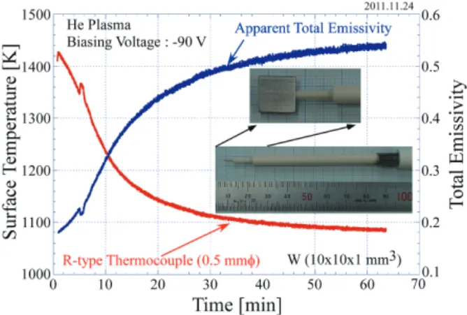
We try to estimate the TE by a change in surface temperature on the way to nanostructure formation. The Stefan-Boltzmann law is invoked by assuming that the fixed biasing of the target does not change the plasma heat flux substantially and that the conduction loss through the thin sheath of the R-type thermocouple with the diameter of 0.5 mm can be almost negligible in such a high temperature range. Figure 1 shows the time evolutions of W temperature in the He plasma with a fixed biasing of – 90 V with respect to the potential of vacuum chamber of AIT-PID together with the photo showing an assembly of the W target and the thermocouple, where the plasma potential is + 5 V. The TE obtained with the relation of et*(t)σ{T*(t)}4S = e
t σT4S ,where the right-hand side corresponds to the virgin W at the start with et =0.18 at this temperature 13)
A similar but different approach is shown in Fig.2 where W with nanostructure was exposed to Ar plasma in AIT-PID which provided a sputtering of W surface leading to a normal flat W with a biasing of - 100 V. The starting and final biasing voltages are the same, - 12V, in between the biasing voltage is set down to – 100 V in order to enhance the sputtering. The TE at the final stage e
. A substantial increase in the TE has been observed. The final value is about 0.54 in the present case. Several similar experiments gave it over the range between 0.45 and 0.55. Here, we assume that the macroscopically geometric surface area does not change with the nanostructure formation. But the microscopic area is effectively increased. However, we do not need to know the exact microscopic surface area because this increase is converted to the radiation emissivity with a constant surface area.
t = 0.14 for the temperature of 1150 K. It is traced back to the original nanostructured tungsten. Again the value for the TE is close to 0.50.
2.2 Electron Beam Method
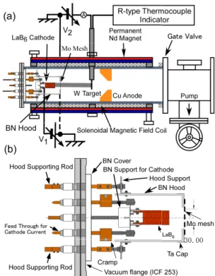
The absolute value of TE has been estimated by a completely different way from the previous method, using the known electron beam power for the same tungsten target in which the thermocouple is inserted. The device for the present purpose is almost the same as AIT-PID as shown in Fig.3(a) under the vacuum condition without any gas feeding, but a small grounded molybdenum mesh (20 meshes/inch) just in front of LaB6 cathode is set at the head of boron-nitride
(BN) hood as shown in Fig.3(b) to pull out the electrons by the voltage of V1 along the axis of vacuum chamber where the multicusp magnetic field intensity is very weak or zero. The electron beam is transported through this region to arrive the W target which is positively biased by V2 with respect to the grounded chamber, Fig. 2 Temporal changes in PM-W temperature measured with thermocouple, biasing current, biasing voltage and calculated apparent total emissivity in the sputtering process in Ar plasma for the originally nanostructured W.
Fig. 1 Time evolutions of the temperature of PM-W (10×10×1 mm3) measured with R-type thermocouple (0.5
mm in diameter) and the corresponding apparent total emissivity deduced Stefan-Boltzmann law on the way to nanostructure formation in He plasma with a fixed biasing voltage.
2. Evaluation of Total Emissivity
The TE is the most appropriate measure for the radiation cooling characteristics. It is well documented for normal W 13), and has been confirmed by an
electron beam calibration 14). However, we do not have
enough evaluations of those for nanostructured W 15, 16).
The experiment has been done in the compact plasma device AIT-PID 17).
2.1 Fixed Biasing Method
We try to estimate the TE by a change in surface temperature on the way to nanostructure formation. The Stefan-Boltzmann law is invoked by assuming that the fixed biasing of the target does not change the plasma heat flux substantially and that the conduction loss through the thin sheath of the R-type thermocouple with the diameter of 0.5 mm can be almost negligible in such a high temperature range. Figure 1 shows the time evolutions of W temperature in the He plasma with a fixed biasing of – 90 V with respect to the potential of vacuum chamber of AIT-PID together with the photo showing an assembly of the W target and the thermocouple, where the plasma potential is + 5 V. The TE obtained with the relation of et*(t)σ{T*(t)}4S = e
t σT4S ,where the right-hand side corresponds to the virgin W at the start with et =0.18 at this temperature 13)
A similar but different approach is shown in Fig.2 where W with nanostructure was exposed to Ar plasma in AIT-PID which provided a sputtering of W surface leading to a normal flat W with a biasing of - 100 V. The starting and final biasing voltages are the same, - 12V, in between the biasing voltage is set down to – 100 V in order to enhance the sputtering. The TE at the final stage e
. A substantial increase in the TE has been observed. The final value is about 0.54 in the present case. Several similar experiments gave it over the range between 0.45 and 0.55. Here, we assume that the macroscopically geometric surface area does not change with the nanostructure formation. But the microscopic area is effectively increased. However, we do not need to know the exact microscopic surface area because this increase is converted to the radiation emissivity with a constant surface area.
t = 0.14 for the temperature of 1150 K. It is traced back to the original nanostructured tungsten. Again the value for the TE is close to 0.50.
2.2 Electron Beam Method
The absolute value of TE has been estimated by a completely different way from the previous method, using the known electron beam power for the same tungsten target in which the thermocouple is inserted. The device for the present purpose is almost the same as AIT-PID as shown in Fig.3(a) under the vacuum condition without any gas feeding, but a small grounded molybdenum mesh (20 meshes/inch) just in front of LaB6 cathode is set at the head of boron-nitride
(BN) hood as shown in Fig.3(b) to pull out the electrons by the voltage of V1 along the axis of vacuum chamber where the multicusp magnetic field intensity is very weak or zero. The electron beam is transported through this region to arrive the W target which is positively biased by V2 with respect to the grounded chamber, Fig. 2 Temporal changes in PM-W temperature measured with thermocouple, biasing current, biasing voltage and calculated apparent total emissivity in the sputtering process in Ar plasma for the originally nanostructured W.
Fig. 1 Time evolutions of the temperature of PM-W (10×10×1 mm3) measured with R-type thermocouple (0.5
mm in diameter) and the corresponding apparent total emissivity deduced Stefan-Boltzmann law on the way to nanostructure formation in He plasma with a fixed biasing voltage.
while the cathode is negatively biased to have an acceleration of electrons. Such a potential configuration may inhibit any release of secondary electrons from the target which ensures that the input power to the target can be calculated by the product of the target current and the acceleration voltage which corresponds to V1 +
V2.
The relations between the target input power and the temperature are shown in Fig.4 for the virgin as well as nanostructured black W with the size of 15x15x1 mm3. In the case of the black W with
fiber-form nanostructure on its surface, a fairly rapid measurement ensures a negligible change in nanostructure coming from a kind of annealing although the maximum temperature is less than 1200 K which is much lower than the temperature for annealing
12, 18), e.g. more than 1600 K. Such a careful
measurement makes the number of data points not so large as those for virgin W. Some small corrections are made for the power balance equation: P = et(T)σST4 + κT – P0 where P0 is the additional power input from LaB6 heat radiation and the second term corresponds to
the conduction loss through the metallic sheath of thermocouple. The data points are well reproduced by the fitted curves. The corrections to the Stephan-Boltzmann relation, κT – P0, are less than 10 % at T ~ 1000 K. The value of κ is 2.0 x 10⁻³W/Κ
and P0 is 2W for virgin W and 3 W for nanostructured W. The temperature dependence formula of total emissivity for virgin W shown in the figure comes from the reference 13). We note that more than 400 K
temperature reductions are detected, which is larger than the temperature changes shown in Figs. 1 and 2. The electron beam calibration gives the TE close to 1.0 corresponding to almost black body for nanostructured W.
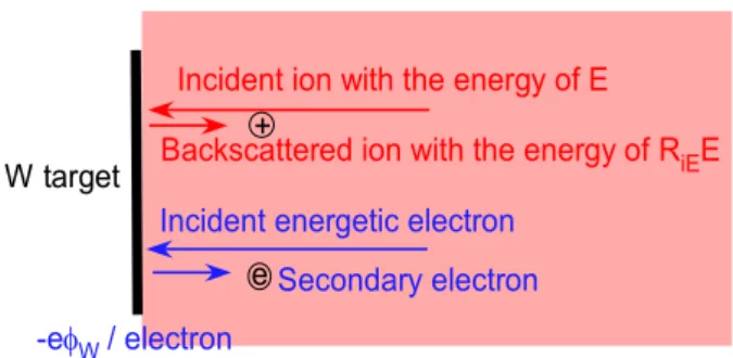
2.3 Discussions on the Difference in Total Emissivity We have to examine the discrepancy between the above two methods to determine the TE. The fixed biasing method assumes that under the fixed biasing the plasma gives the same power input to the target even on the way to surface modification. A schematic view for the power into the target due to ions and electrons is shown in Fig.5 where RiE is the ion energy reflection coefficient on the tungsten surface and φw is the
tungsten work function. Therefore, 1 - RiE is the fraction of ion kinetic energy given to the surface. If the ion energy reflection coefficient on both samples is commonly zero or equal and there is no SEE, then we are certain that the power inputs are the same for both kinds of tungsten. However, the ion energy reflection coefficient would be different between these two which have different surface morphologies. Recently, it was found that the nanostructured W gives a smaller ion energy reflection coefficient compared with the flat tungsten without nanostructure 19). In addition we have
energetic electrons which may generate SEE 17).
Secondary electrons may come out to the surface from the metallic bulk by consumption of the energy Fig. 3 Schematic diagram of electron beam calibration
system using AIT-PID (a) and electron beam source (b).
Fig. 4 Relation between the temperature T and the input power P for virgin tungsten as well as blackened one with the nanostructure, obtained with the electron beam calibration system.
corresponding to the work function, ~4.54 eV in the present case. As mentioned above, deep troughs produced by fiber-form nanostructure makes the incident ion kinetic energy to be consumed much more by multi-collisions with nano-fibers compared with a simple reflection from the flat normal surface. According to the suppression of SEE, we can say that the nanostructured W gets more plasma heat power than the flat normal W does under the same biasing condition. We may write Pv = etvσTv4S for virgin W and PB = etBσTB4S for the final stage of nanostructure formation in Fig.1 by neglecting a small heat conduction loss. The relation, etB = etv(Tv/ TB)4(PB / Pv), is derived. For the case that PB > Pv as discussed above, then we must say an underestimation of TE for the fixed biasing method. It means that the plasma heat loads Pv and PB must be determined precisely by taking account of various surface effects, like ion energy reflection, SEE, and so on. Therefore, it is recognized that the sheath voltage dependence of power transmission factor is very important, especially those for nanostructured as well as virgin W surface in plasmas with high energy electron component.
3. Recovery and Mitigation 3.1. Dust Formation
One of the serious issues for the W with the fiber-form nanostructure is a dust formation. It seems that so called “fuzz” may easily peel off due to a mechanical or a thermal shock. In fact an adhesive carbon tape on the defected W sticks the nanostructure easily as shown in Fig.6(a). Instead these structures can be shaved also easily with a cutting knife. A shaved
surface is shown in Fig.6(b) where many holes can be seen over all the shaved area, and a remain of nanostructure can be seen at the edge of upper right. The dust thus collected is also shown in Fig.6(c) and (d). A kind of fragility has been demonstrated in these treatments.
3.2. Recovery
If we can develop a recovery technique from defected W to normal W, it could be beneficial. With respect to recovery towards the normal flat surface, preferably without any bubbles inside, the argon plasma annealing technique has been employed, in which the W surface temperature was elevated up to around 1850 K by making the target potential towards the plasma potential for the exposure time of 25 min 18). The
plasma heat comes mainly from electrons, while the ion energy is too low to have a sputtering. This idea was based on the effect of temperature excursion on the W surface morphology, that is, shrinkage and fattening of W fibers on the surface 6). The technique has been
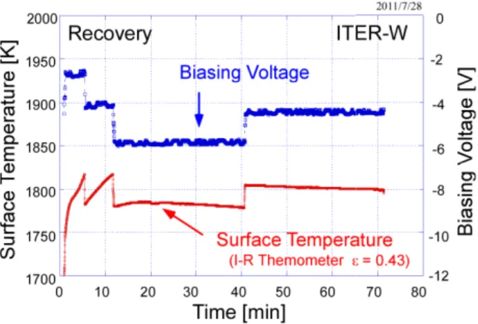
extended to the case of He plasma annealing with the surface temperature of 1800 K for 60 min by the electronic heat load with a small sheath voltage less than 6 V in order to avoid additional formation of bubbles/holes 12, 20)
Figure 7 shows time evolutions of the biasing voltage and the surface temperature over the recovery process
.
Incident ion with the energy of E
Backscattered ion with the energy of R+ iEE Incident energetic electron
eSecondary electron -eφW/ electron
W target
Plasma
Fig. 5 Schematic diagram showing the energy input and output mechanisms at the target due to plasma ion and electron incidences. RiE is the ion energy reflection
coefficient and φw is the work function.
Fig. 6 Possibility of W dust formation from nanostructured W. (a) Nano-fibers peeled off from it on an adhesive carbon tape, (b) shaved W surface with cutting knife, (c) collected W nano-fibers and (d) the magnified view.
corresponding to the work function, ~4.54 eV in the present case. As mentioned above, deep troughs produced by fiber-form nanostructure makes the incident ion kinetic energy to be consumed much more by multi-collisions with nano-fibers compared with a simple reflection from the flat normal surface. According to the suppression of SEE, we can say that the nanostructured W gets more plasma heat power than the flat normal W does under the same biasing condition. We may write Pv = etvσTv4S for virgin W and PB = etBσTB4S for the final stage of nanostructure formation in Fig.1 by neglecting a small heat conduction loss. The relation, etB = etv(Tv/ TB)4(PB / Pv), is derived. For the case that PB > Pv as discussed above, then we must say an underestimation of TE for the fixed biasing method. It means that the plasma heat loads Pv and PB must be determined precisely by taking account of various surface effects, like ion energy reflection, SEE, and so on. Therefore, it is recognized that the sheath voltage dependence of power transmission factor is very important, especially those for nanostructured as well as virgin W surface in plasmas with high energy electron component.
3. Recovery and Mitigation 3.1. Dust Formation
One of the serious issues for the W with the fiber-form nanostructure is a dust formation. It seems that so called “fuzz” may easily peel off due to a mechanical or a thermal shock. In fact an adhesive carbon tape on the defected W sticks the nanostructure easily as shown in Fig.6(a). Instead these structures can be shaved also easily with a cutting knife. A shaved
surface is shown in Fig.6(b) where many holes can be seen over all the shaved area, and a remain of nanostructure can be seen at the edge of upper right. The dust thus collected is also shown in Fig.6(c) and (d). A kind of fragility has been demonstrated in these treatments.
3.2. Recovery
If we can develop a recovery technique from defected W to normal W, it could be beneficial. With respect to recovery towards the normal flat surface, preferably without any bubbles inside, the argon plasma annealing technique has been employed, in which the W surface temperature was elevated up to around 1850 K by making the target potential towards the plasma potential for the exposure time of 25 min 18). The
plasma heat comes mainly from electrons, while the ion energy is too low to have a sputtering. This idea was based on the effect of temperature excursion on the W surface morphology, that is, shrinkage and fattening of W fibers on the surface 6). The technique has been
extended to the case of He plasma annealing with the surface temperature of 1800 K for 60 min by the electronic heat load with a small sheath voltage less than 6 V in order to avoid additional formation of bubbles/holes 12, 20)
Figure 7 shows time evolutions of the biasing voltage and the surface temperature over the recovery process
.
Incident ion with the energy of E
Backscattered ion with the energy of R+ iEE Incident energetic electron
eSecondary electron -eφW/ electron
W target
Plasma
Fig. 5 Schematic diagram showing the energy input and output mechanisms at the target due to plasma ion and electron incidences. RiE is the ion energy reflection
coefficient and φw is the work function.
Fig. 6 Possibility of W dust formation from nanostructured W. (a) Nano-fibers peeled off from it on an adhesive carbon tape, (b) shaved W surface with cutting knife, (c) collected W nano-fibers and (d) the magnified view.
for the ITER-grade W which has the same production procedure as for PM-W (Powder Metallurgy Tungsten), but the plasma-facing surface is perpendicular to the compressed layers. A spontaneous increase in surface temperature at the beginning with a fixed biasing voltage comes from the reduction in the total emissivity of W surface due to plasma annealing. After sufficient plasma annealing, we have a steady temperature.
Figure 8 shows surface morphologies of ITER-grade W observed with FE-SEM, where (a) shows a virgin surface as well as a photo of whole target. We can distinguish many parallel lines on the surface coming from pressed layers. Figure 8(b) shows a surface morphology made of fiber-form nanostructure, and a photo of the black target. A recovery is shown in Figs.8(c) and (d) with different magnifications together with a photo of a silver-colored recovered W target. We can distinguish some tiny holes although an apparent flat surface has been recovered.
Figure 9 shows some examples of recovered surfaces as well as original fiber-form nanostructured surface. Recovered surface for PM-W is shown in Fig.9(b), and advanced W material TFGR-W 1.1%TiC/H (Toughing, Fine-Grained Recrystalized W with TiC dispersoid) 21) is also shown in Fig.9(c),
obtained by the same plasma annealing condition as for PM-W. The recovery for TFGR-W is somewhat incomplete 12). Concerning ITER-grade W, it has a
recovery property similar to the normal PM-W. The recovered ITER-grade W has also similar bubbles with 50 ~ 100 nm in diameter under about 100 nm in depth.
Fig. 7 Temporal evolutions of the biasing voltage and the surface temperature measured with IR-thermometer for ITER-grade W with fiber-form nanostructure originally on its surface on the way to recovery of the surface.
Fig. 8 FE-SEM images for ITER-grade tungsten. (a) Virgin surface. The photo is inserted. (b) Nanostructure formed on the target (a) with the photo of black target. (c) and (d) Recovered surfaces which contains some holes on its surface. The photo is inserted.
Fig. 9 Original fiber-form nanostructured and plasma annealed W surfaces. (a) Nanostructure of He-defected PM-W due to He plasma irradiation where (a-1) shows a top surface and (a-2) is its cross-section. (b) recovered structure of PM-W where (b-1) is the top surface and (b-2) grazing view, and (c-1) and (c-2) are recovered top views for TFGR-W with different magnifications.
3.3. Mitigation
The most effective way against the formation of nanostructure on the W surface is to suppress the formation process itself. One way for the suppression is to make a thin carbon layer on the tungsten surface which prevents the helium ions to arrive at the tungsten. The thickness of carbon layer must be sufficiently large compared with the penetration depth of helium ions which is a few tens nanometer at most. The physical sputtering of carbon with He ion bombardment may dissipate the carbon layer. For example, the sputtering yield for 100 eV He is about 0.03. In addition, the chemical sputtering due to hydrogen ions may increase the erosion of carbon layer. Here, we try to demonstrate the principle of mitigation with carbon thin film. Figure 10 shows the schematic drawing of the system producing the carbon film formation on the W target with an introduction of methane gas into He plasmas. The best condition has been looked for by changing the CH4 gas flow rate and deposition time in helium – methane mixed gas discharge as shown in Table 1. The standard operation condition for the carbon film deposition is as follows: the He gas flow rate: 70 sccm, the CH4 gas flow rate: 0.5 sccm, the discharge current Id = 7.5 A and the deposition time is 60 min. The starting surface temperature is about 1240 ~ 1280 K, but the final temperature decreases down to 990 ~ 940 K due to radiation cooling caused by an increase in radiation emissivity.
Figure 11 shows the cross-section of carbon layer on the thin (35 µm) W plate. The thickness of 500 nm carbon film was found to be formed under the above mentioned standard operation. The carbon coated thick W target with R-type thermocouple (0.5 mmφ) was exposed to a pure He plasma with the discharge current of Id = 15 A, He gas flow rate of 70 sccm and the biasing voltage of -40 V (the ion incident energy: 45 eV), which is a typical He plasma condition producing a fiber-form nanostructure for virgin W without carbon layer. The typical temperature history measured with R-type thermocouple is shown in Fig.12, showing the temperature of 1120 to 1180 K. We confirmed no nanostructure formation on this sample as shown by the SEM photo inserted in Fig.12.
In order to demonstrate more clearly, the following procedure has been employed. First, a W sample of 10×10×0.1 mm3 was covered with another
Permanent Magnet ICF70
Port
Cooling Water Solenoidal Winding
Target
Bellows Vacuum Chamber
Port ICF70
CH4
Ceramic cove with SUSTube
Fig. 10 Schematic drawing of the system producing thin carbon film formation on the W target with an introduction of methane gas.
Table 1 Experimental conditions for the formation of protective carbon film against the fiber-form nanostructure growth on W surface.
Fig. 11 FE-SEM photo showing the cross-section of W substrate deposited by carbon layer under the standard condition.
thin W in a reduced size of10×7×0.035 mm3. This double W sample was exposed to He (70 sccm) and methane(0.5 sccm) mixed gas discharge plasma with the discharge current of 7.5 A and the target biasing of -15 V for one hour to have a carbon film coating on the whole surface.
Then, the thin cover W is removed to have a fresh W area. The sample with two areas was exposed to pure He plasma with a biasing voltage of -40 V for two hours with the surface temperature of 1100 K. The macroscopic view for the sample after He plasma exposure is shown in Fig.13 where the black area has a nanostructure while the gray one does not.
Figure 14 shows microscopic views for the above sample, where (a) and (c) show the cross-section, and (b) and (d) are grazing views for these areas. Now, the thickness of carbon layer decreased from about 500 nm down to 140 nm probably due to sputtering by helium ions. We found that the carbon thin layer protect against the formation of nanostructure. Such an inhibition of fuzz structure formation was originally reported by PISCES group 22). Here a more visual way has been demonstrated.
4. Summary and Conclusion
Precise estimation for the radiation capability of nanostructured W has been obtained in terms of total emissivity (TE) by using electron beam calibration system in vacuum. The black nanostructured W surface was found to play as an almost complete black-body. The questions related to the fixed biasing method for obtaining the TE are discussed in terms of ion energy reflection and a cooling associated by SEE. It is recognized that the power transmission factor through the plasma sheath is very important, especially for the surface with a change in surface morphology.
The unfavorable property of such He-defected W are discussed from the points of view of dust formation. Some recovery process to obtain an original flat surface are represented focusing on the ITER grade PM-W although the tiny bubbles remain underneath the surface, and thin carbon coating with the thickness of a few hundreds nanometer is demonstrated to represent a kind of protective layer against the formation of He Fig. 12 Pure He plasma exposure on carbon coated tungsten
prepared with the standard carbon deposition condition. Insertion shows the FE-SEM photo showing no nanostructure formation after pure He plasma exposure for two hours.
Fig. 13 Photo of W surface where two areas of fiber-form nanostructure are developed, black one with fiber-form nanostructure and gray zone without nanostructure. The size of PM-W sample is 10×10×0.1 mm3.
Fig. 14 FE-SEM photos for two areas seen in Fig.13. Here (a) and (b) show the top and grazing views of black zone, while (c) and (d) do those at gray zone.
defects. In the case of ITER, beryllium would take a place of carbon.
Acknowledgements
The research work was supported by Grant-in-aid for Scientific Research (B) 20360414, Grant-in-Aid for Challenging Exploratory Research 23656578, and Grant-in-aid for Scientific Research (A) 2246120 from JSPS, and also by The Science Research Promotion Fund from the Promotion and Mutual Aid Corporation for Private School of Japan. The authors would like to thank H. Iwata of AIT for his help on FE-SEM manipulation and Dr. S. Kajita of Nagoya University for his valuable discussions.
References
1) S. Takamura, N. Ohno, D. Nishijima and S. Kajita, “Formation of Nanostructured Tungsten with Arborescent Shape due to Helium Plasma Irradiation”, Plasma Fusion Res. Vol.1, 051(2 pages), 2006.
2) M.J. Baldwin and D.P. Doerner, “Helium induced nanoscopic morphology on tungsten under fusion relevant plasma conditions”, Nucl. Fusion Vol.48, pp.035001, 2008.
3) G.M. Wright, D. Brunner, M.J. Baldwin, R.P. Doerner, B. Labombard, B. Lipschultz, J.L. Terry and D.G. Whyte, “Tungsten nano-tendril growth in the Alcator C-Mod divertor”, Nucl. Fusion Vol.52, pp.042003(5 pages), 2012.
4) S. Takamura, T. Miyamoto and N. Ohno, “Outstanding properties of tungsten material with fiber-fom nanostructured subsurface for the wall of fusion reactor”, Proc. 38th EPS Conf. on Plasma
Physics (Strasbourgh, France 27 June-1 July 2011) O1-302
http://ocs.ciemat.es/EPS2011PAP/pdf/O1.302.pdf, 2011.
5) S. Takamura, T. Miyamoto and N. Ohno,” Effects of fibre-form nanostructures on particle emissions from a tungsten surface in plasmas”, Nucl. Fusion Vol.52, pp.123001(8 pages), 2012.
6) S. Takamura, T. Miyamoto, Y. Tomida, T.
Minagawa and N. Ohno, “Investigation on the effect of temperature excursion on the helium defects of tungsten surface by using compact plasma device”, J. Nucl. Mater. Vol.415, pp.S100(4 pages), 2011.
7) S. Takamura, T. Miyamoto and N. Ohno, “Deepening of Floating Potential for Tungsten Target Plate on the way to Nanostructure Formation”, Plasma Fusion Res. Vol.5, pp.039(2 pages), 2010.
8) D. Nishijima, Y. Kikuchi, M. Nakatsuka, M.J. Baldwin, R.P. Doerner, M. Nagatsa and Y. Ueda, “Effects of Steady-State Plasma Exposure on Tungsten Surface Cracking due to Elm-Like Pulsed Plasma Bombardment”, Fusion Sci. Technol. Vol.60 pp.1447-1450, 2011.
9) Y. Kikuchi, D. Nishijima, M. Nakatsuka, K. Ando, T. Higashi, Y. Ueno, M. Ishihara, K. Shoda, M. Nagata, T. Kawai, Y. Ueda, N. Fukumoto and R.P. Doerner, “Surface damage characteristics of CFC and tungsten with repetitive ELM-like pulsed plasma irradiation”, J. Nucl. Mater. Vol.415, pp.S55-S58, 2011.
10) S. Kajita, S. Takamura and N. Ohno, “Prompt ignition of a unipolar arc on helium irradiated tungsten”, Nucl. Fusion Vol.49 pp.032002(4 pages), 2009.
11) M. Tokitani, S. Kajita, S. Masuzaki, Y. Hirahara, N. Ohno, T. Tanabe and LHD Experiment Group, “Exfoliation of the tungsten fibreform nanostructure by unipolar arcing in the LHD divertor plasma ”, Nucl. Fusion Vol.51, pp.102001(5 pages), 2011.
12) T. Miyamoto, S. Takamura and H. Kurishita, “Recovery of Tungsten Surface with Fiber-Form Nanostructure by Plasmas Exposures”, Plasma Sci. Technol. Vol.15, pp.161-165, 2013.
13) E. Lassner and W.D. Schubert, “TUNGSTEN”, Kluer Academic / Plenum Publishers, New York, 1999.
14) S. Takamura, T. Miyamoto and N. Ohno, “Thermal Radiation Characteristics and Direct Evidence of Tungsten Cooling on the way to Nanostructure Formation on Its surface”, 20th Int.
Conf. on Plasma-Surface Interactions in Controlled Fusion Devices, May 21-25, 2012, Aachen,
Germany, p2-056, J. Nucl. Mater. Vol.438, pp.S814-S817, 2013.
15) S. Kajita, T. Yokochi, N. Ohno and T. Kumano, “Near Infrared Radiation from Heated Nanostructured Tungsten”, Jpn. J. Appl. Phys. Vol.51, pp.01AJ03(5 pages), 2012.
16) S. Kajita, N. Ohno, T. Yokochi, N. Yoshida, R. Yoshihara, S. Takamura and T. Hatae, “Optical properties of nanostructured tungsten in near infrared range”, Plasma Phys. Control Fusion Vol.54, pp.105015(), 2012.
17) S. Takamura, “Characteristics of Compact Plasma Device AIT-PID with Multicusp Magnetic Confinement”, IEEJ Trans. on E. E. Eng. Vol.7(S1), pp.S19-S24, 2012.
18) S. Takamura and T. Miyamoto, “Recovery of Tungsten Surface with Fiber-Form Nanostructure by the Argon Plasma Irradiation at a High Surface Temperature”, Plasma Fusion Res. Vol.6, pp.005(2pages), 2011.
19) S. Takamura, T. Miyamoto and N. Ohno, “POWER TRANSMISSION FACTOR FOR TUNGSTEN TARGET W/WO FIBER-FORM NANOSTRUCTURE IN HE PLASMAS WITH HOT ELECTRON COMPONENT USING COMPACT PLASMA DEVICE AIT-PID”, Joint Conference of OS2012 and PMIF 2012, August 27-31, 2012, Tsukuba, Japan, Fusion Sci. Technol. Vol.63, No.1T, pp.225-228, 2013.
20) S. Kajita, N. Yoshida, R. Yoshihara, N. Ohno, T. Yokochi, M. Tokitani and S. Takamura, “TEM analysis of high temperature annealed W nanostructure surfaces“, J. Nucl. Mater. Vol.421, pp.22-27, 2012.
21) H. Kurishita, S. Matsuo, H. Arakawa, T. Sakamoto, S. Kobayashi, K. Nakai, T. Tokida, M. Kato, M. Kawai and N. Yoshida, “Development of re-crystallized W–1.1%TiC with enhanced room-temperature ductility and radiation performance”, J. Nucl. Mater. Vol.398, PP.87-92, 2010.
22) M.J. Baldwin, R.P. Doerner, D. Nishijima, K. Tokunaga and Y. Ueda, “The effects of high fluence mixed-species (deuterium, helium, beryllium) plasma interactions with tungsten”, J. Nucl. Mater. Vol.390-391, pp.886-890, 2009.