Serial Lecture
Photoemission Electron Spectroscopy II:
Satellites by Local Excitations
(Author) J. D. Leea,*
(Translator) T. Nagatomib and G. Mizutania (Translation Supervisor) K. Endoc
aSchool of Materials Science, Japan Advanced Institute of Science and Technology, Ishikawa 923-1292, Japan bDepartment of Material and Life Science, Graduate School of Engineering, Osaka University,
Suita, Osaka 565-0871, Japan
cCenter for Colloid and Interface Science, Tokyo University of Science, Noda, Chiba 278-8510, Japan *[email protected]
(Received: September 1, 2009)
Photoemission process leaves the target system in various final states that are lacking one electron with respect to the initial state. Except for the trivial noninteracting case, the final-state effects result in separate features in the photoemission electron spectra (PES). They are distinguished as the main feature and its sat-ellites. Knowledge about those features for a given material is fundamentally important in understanding the electronic property of the material. We discuss the main and satellite features signaled in PES especially when the final states are reached by the local excitations, usually corresponding to the atoms, molecules, or strongly correlated electron solids like transition metal or rare earth metal compounds or several organic compounds. In particular, we focus on a few famous and prototypical PES problems of transition metal compounds (i.e., 3d-valence insulators, or sometimes narrow band 3d metals) and their understanding.
光電子分光法
II 局所励起によるサテライト
(著者) J. D. Leea,* (日本語訳者) 永富隆清,b,** 水谷五郎a,*** (監訳者) 遠藤一央c,**** a北陸先端科学技術大学院大学 マテリアルサイエンス研究科 〒923-1292 石川県能美市旭台 1-1 b大阪大学 大学院工学研究科 生命先端工学専攻 物質生命工学講座 〒565-0871 大阪府吹田市山田丘 2-1 c東京理科大学 総合研究機構 界面科学研究センター 〒278-8510 千葉県野田市山崎 2641 *[email protected] ** [email protected] *** [email protected] ****[email protected] (2009 年 9 月 1 日受理) 光電子を放出した後の試料内原子は,初期状態に比べて電子が一つ少ない終状態をとる.この 終状態には様々な状態があるため,終状態に存在する正孔と電子が相互作用しない場合を除いて, 光電子スペクトル(PES)にはサテライト構造が見られる.これらサテライトピークは主ピーク と区別される.ある材料系におけるサテライト構造に対する知見は,材料の電子状態を理解する ための基本として重要である.本稿では,特に局在化した励起過程を経て終状態に至る場合にPES において見られる主ピークとサテライトピーク構造について議論する.これらは,原子,分子,あるいは遷移金属や希土類金属の化合物,いくつかの有機材料などの強相関電子系固体において
見られる現象である.本稿では特に,遷移金属化合物(すなわち,3d 価電子絶縁体,あるいは狭
バンド3d 金属)に見られるいくつかの有名で基本的な PES 問題とその解釈について述べる.
1. Introduction
Photoemission electron spectroscopy (PES) produces final states which are lacking one electron with respect to the initial ground state and measures their energies [1]. The energies measured in PES are, of course, the hole-state energies and depend on the final-state con-figurations, and thus they are generally different from the single-electron orbital energies in the ground state of the material. The utmost origin of such nontrivial final-state effects is the electron correlation by the Coulomb inter-action, which is met in the many-body systems. It should be noted that atoms, molecules, and solids are many-body systems.
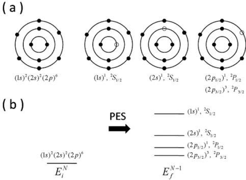
Emission of one electron by the PES process must lead to nontrivial effects in the remaining system, i.e., the final-state effects. The most elementary example of the final-state effect in the PES would be found in an argu-ment of the binding energy of the atomic orbital. In Fig. 1, the simple PES processes for Ne atom which has three atomic orbitals containing electrons are displayed. The
PES measures the energy difference between the initial ground state energy with N electrons EiN and the final state with N-1 electrons EfN-1 and gives the binding en-ergy EB as EB=EfN-1-EiN. Neglecting the electronic rear-rangement such as the orbital relaxation, the binding en-ergy is stated to equal the negative enen-ergy of the orbital from which the photohole is created. From Fig.1, for the
orbitals of Ne, one may have N
s E s E1 1 1 [(1 )] , N s E s E1 1 2 [(2 ) ] , N p E p E1 1 2 / 1 2 1/2 [(2 ) ] , and N p E p E1 1 2 / 3 2 3/2 [(2 )]
, where the splitting between
2p1/2 and 2p3/2 is due to the spin-orbit coupling between the unpaired spin and orbital angular momentum. This is known as the Koopmans’ approximation [2], or a “bare” or “undressed” hole in solid state terminology. Another important example regarding the atomic binding energy is the chemical shift, the change in the binding energy between two different chemical environments surround-ing the same atoms.
Fig. 1. (a) Schematic illustration of the initial state and final states (depending on the orbital where the electron is ejected) before and after the PES of Ne atom. (b) Energy levels corresponding to the initial state and final states. Due to the spin-orbit coupling, 2p3/2 and 2p1/2 would be split. Closed dots represent the electrons and the open dots the photoholes, respectively.
1. はじめに 光電子分光法(PES)では,始状態である基底状 態に比べて電子が一つ少ない終状態が形成され,そ れらの状態のエネルギーを測定する[1].PES で測定 されるエネルギーは正孔が存在する状態でのエネル ギーであるため終状態の電子配置に依存し,物質の 基底状態での1 電子軌道エネルギーとは一般に異な る.そのような終状態に正孔が存在することによっ て引き起こされる効果の最大の起源はクーロン相互 作用による電子相関であり,多体系において見られ る効果である.ここで原子,分子や固体は多体系で ある. PES 過程における 1 電子放出は,残った系,すな わち終状態に大きな影響を与える.PES における終 状態効果の最も基本的な例は,原子軌道の結合エネ ルギーに関する議論である.図1 は 3 つの原子軌道 を持つNe 原子に対する単純な PES 過程を示してお り,軌道に存在する電子も示してある.PES では, N 個の電子が存在している始状態である基底状態の エネルギーEiNと電子数が N-1 個である終状態のエ ネルギーEfN-1 の差を結合エネルギーEB=EfN-1-EiNと して測定する.電子軌道の緩和などの電子の再配列 を無視すると,光正孔が生成された軌道の負のエネ ルギーに結合エネルギーは等しくなる.図1 より, Ne の 軌 道 に 対 し て , N s E s E1 1 1 [(1)] , N s E s E1 1 2 [(2 )] , N p E p E1 1 2 / 1 21/2 [(2 )] 及 び N p E p E1 1 2 / 3 2 3/2 [(2 )] が得られる.ここで 2p1/2 と 2p3/2の分裂は,ペアーを作っていないスピンと軌道 角運動量の間のスピン-軌道相互作用によって生じ る.これはKoopmans 近似[2],あるいは,固体物理 の用語では「裸の」正孔として知られている.原子 の結合エネルギーに関するもう一つの重要な例は, ある元素を考えた場合に,原子周辺の化学的環境が 異なるとその元素の結合エネルギーも異なるという 化学シフトである.
More explicit electron correlation could be discussed through the excited states of the remaining system led to by the photohole created in the PES process. Except for the particular cases like valence states of wide-band sol-ids (e.g., the free-electron final state model is well ap-plied for the valence states of Cu metal [3]), the photo-hole is generally not fully screened. The core-level PES creates final states with spin and orbital angular momen-tum. In particular, if the system has the open valence configuration, the spin of the photohole can couple par-allel or antiparpar-allel to the spin of the outer valence con-figuration. This gives the exchange splitting at given atomic levels, so called the core polarization. It is possi-ble to specify the spectral lines into the final state with lower energy and higher energy by the exchange split-ting.
Satellite (also called shake-up structure) in the core level PES has been a research area of intensive and ex-tensive theoretical and experimental efforts [4,5]. The Coulomb interaction felt by the valence electrons when a core-level electron is ejected in the PES causes their screening collapse towards the positive photohole, lead-ing to the excitations of the remainlead-ing system. These excitations require energy and give the photoelectron signals with smaller kinetic energies (larger binding en-ergies) than the signal corresponding to the ground state. Therefore, in a general sense, the PES consists of a main line (corresponding to the ground state after the PES, i.e., no-loss line) and several features of satellites (corre-sponding to excited states, i.e., loss lines). Except for a noninteracting system (or simply a system where the photohole is completely screened), satellites could be observed as lines additional to the main line in any in-teracting system. Satellite structures observed in com-pounds of transition metals or rare earth metals, alakali metal halides, and several organic compounds are espe-cially interesting and important because they deliver abundant physics of the electron correlation. Such elec-tron correlation is believed to play a central role in the most attractive materials of the solid state physics or materials science, like high Tc superconductors. In these cases, the satellites are usually excited through the charge-transfer excitation between outer valences or the Mott excitation between d electrons, which will be dis-cussed later. These charge-transfer or Mott excitations are distinguished from the core polarization and they
could occur together with the core polarization without interference.
A photohole left raises, in principle, various kinds of excitations in the remaining system, for instance, the charge excitations, the spin excitations, vibrational (nu-clear) excitations, and so on. Some would be the local excitations, i.e., the atomic-like excitations of charges, spins, and vibrations, while others would be the extended excitations, i.e., the collective excitations of charges, spins, and vibrations (in other words, plasmons, magnons, and phonons). Physics of satellites would be very differ-ent depending on the local or extended excitations. In this issue, we mainly treat the satellites by the local ex-citations, which are usually relevant in the compounds including 3d transition metal elements or rare-earth ele-ments and incorporating the strong electron correlation. The satellite by the extended excitations would be treated in the next issue of this serial lecture.
2. Elementary multiplet splitting
The multiplet splitting generally constructs the most essential interpretation of the PES by characterizing the binding energies of the excited states of the system. As an origin of the elementary line-splitting, we firstly in-troduce the spin-orbit coupling. For Ar atom, the final state after making a hole in the outer p orbital has (3p)5 configuration so that the unpaired spin and orbital angu-lar momentum couple to each other. In Fig. 2, the PES of Ar gas gives the simplest structure of the split features of 3p3/2 and 3p1/2 with the statistical weight in the ratio 2:1 (2×3/2+1: 2×1/2+1) by the spin-orbit coupling because the gaseous phase does not contain other possible excita-tions to make several substructures in the spectra, e.g., vibrational excitation. The general features of the spin-orbit splitting of the core-level PES would be un-derstood as follows; (i) the s orbital is not split, giving a singlet, (ii) the p, d, f, … orbitals are split, giving a dou-blet, (iii) a state with lower j-value has higher binding energy (see Fig. 2; we find that 3p1/2 has higher binding energy than 3p3/2), and (iv) the splitting increases with the atomic number.
より明確な電子相関は,PES 過程によって生成さ れた光正孔に起因して励起された終状態を考えるこ とで議論できる.バンド幅の広い固体の価電子状態 (例えば自由電子終状態モデルでよく記述できる金 属Cu の価電子状態[3])のような特別な場合を除い て,光正孔は一般には完全に遮蔽されない.内殻PES では,スピンと軌道角運動量を持つ終状態が生成さ れる.特に,対象とする系が閉殻でない価電子配置 を持つ場合,光正孔のスピンは外側の価電子配置の スピンと相互作用して,平行あるいは反平行スピン を持つことになる.これは,ある原子準位において 交換分裂,いわゆる内殻分極を引き起こし,スペク トルに見られる分裂したピークは,この交換分裂に よって生じたエネルギーが低い終状態と高い終状態 のそれぞれに帰着することができる. 内殻PES に見られるサテライト(シェークアップ とも呼ばれる)は理論的,実験的研究が精力的に行 われている研究分野である[4,5].PES 過程で内殻電 子が放出された後に価電子が感じるクーロン相互作 用によって正の電荷を持つ光正孔に対する遮蔽が崩 れ,その結果,励起された終状態が形成されること になる.これらの励起にはエネルギーが必要であり, 基底状態の結合エネルギーから求めるよりも低い運 動エネルギー(高結合エネルギー)を持つ光電子が 生成されることになる.それゆえ,PES で観測され るピークは一般的に,主ピーク(PES 過程後の基底 状態に相当する,すなわちノーロスピーク)といく つかのサテライトピーク(励起状態に相当する,ロ スピーク)で形成されることになる.相互作用しな い系(あるいは単に光正孔が完全に遮蔽された系) を除いて,相互作用が存在する系の全てにおいて, 主ピークに加えてサテライトピークが観測される. 遷移金属や希土類金属化合物,アルカリハライド, いくつかの有機化合物において見られるサテライト 構造は,電子相関に関する多くの物理現象を含むこ とから,特に興味深く重要である.そのような電子 相関は,例えば高温超電導体など,固体物理学や物 質科学において最も重要で魅力的な物質において中 心的な役割を果たしていると考えられている.これ らの場合,サテライトは通常,外側の価電子の間の 電荷移動励起や d 電子間の Mott 励起などの過程に よって励起される.これらの過程については後述す るが,これら電荷移動やMott 励起は内殻分極と区別 され,内殻分極と互いに干渉することなく同時に起 きる可能性がある. 原理的には,残った光正孔は,例えば電荷の励起, スピンの励起,(核)振動励起などの様々な種類の励 起を起こす.いくつかの励起過程は局所的な励起, すなわち電荷やスピン,振動などの原子に局在した 励起を起こし,他の励起過程では空間的に広がった 励起,すなわち電荷やスピン,振動の集団励起(い わゆる,プラズモン,マグノン,フォノン)を引き 起こす.サテライトに関する物理は,局所的な励起 か空間的に広がった励起かのいずれによって生じる かで全く異なる.本稿では,局所的な励起によって 生じるサテライトを主に扱う.これらは通常,3d 遷 移金属元素や希土類元素を含む化合物で見られる現 象で,強電子相関と関連している.空間的に広がっ た励起によるサテライトは,本連載の次回に取り扱 う予定である. 2. 基本的な多重項分裂 多重項分裂は一般にPES におけるサテライトの起 源の最も基本的な解釈であり,その分裂エネルギー は励起状態にある系の結合エネルギーによって説明 される.PES ピークの分裂の起源として,まずスピ ン-軌道相互作用を導入する.Ar 原子の場合,外側 のp 軌道に正孔が生じた後の終状態は (3p)5 の電子 配置をとるため,ペアーを作っていないスピンと軌 道角運動量の相互作用が起きる.図 2 に Ar 気体に 対して観測されるスピン-軌道相互作用によって 3p3/2と3p1/2が分裂した最も単純なスペクトルを示す. ガス状物質のPES ではスピン-軌道相互作用以外に サテライトを形成する可能性のある過程,例えば振 動励起などが存在しないため,これらのピークの統 計的な重みは2:1(2×3/2+1: 2×1/2+1)である.内殻 PES に見られるスピン-軌道相互作用による分裂の 一般的な特徴は次の通りである.(i) s 軌道は分裂せ ず一重項である,(ii) p,d,f,...軌道は分裂して二 重項を与える,(iii) 低い j 値を持つ状態は高い結合 エネルギーを持つ(図2 参照,3p1/2のほうが3p3/2よ りも高い結合エネルギーを持つことが分かる),(iv) 原子番号の増加に伴って分裂のエネルギーが増大す る.
Unlike the monoatomic gas (e.g., Ar gas), for the dia-tomic molecule, the vibrational or rotational excitations of the nuclei are inherent in the PES process. A part of the kinetic energy of the escaping electron can be ab-sorbed in the excitation of vibration or rotation of the nuclei. Therefore, the kinetic energy Ek of the escaping electron satisfies -Ek=EB+Evib+Erot, where is the
photon energy and Evib and Erot are vibrational and rota-tional excitation energies, respectively. The relation represents several high binding energy features beyond the fundamental binding energy EB (or the ionization potential energy for a given orbital). The energy distribu-tion and spectral weights of those high binding energy features are determined by the Franck-Condon problem [6].
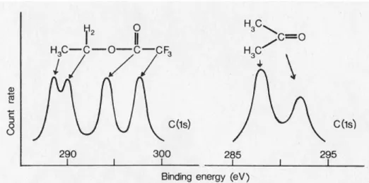
Another kind of elementary multiplet splitting would be found in the chemical shift. As mentioned previously, the binding energy in the PES not only depends on the atomic level where the electron is ejected but also the local chemical environments. Therefore, the chemical shift would be useful to identify the chemical environ-ment of an eleenviron-ment. For this purpose, the electron spec-troscopy for chemical analysis (ESCA) has been devel-oped through the core-level PES [8]. Figure 3 shows that the PES line of an element (C 1s) is found to vary over a few electron volts according to the state of chemical combination of the atom and the nature of its immediate neighbors. The binding energies of a given atomic level under various chemical coordination are tabulated in the available databases [9].
Fig. 2. PES of Ar gas with Ne I source (16.85 eV). 3p3/2 and
3p1/2 are split with the weight ratio 2:1 due to the spin-orbit
coupling. The figure is taken from Ref. 7.
Fig. 3. C 1s core-level PES in ethyl trifluoroacetate (left panel; CF3CO2C2H5) and acetone (right panel; (CH3)2CO). The figure is
Ar などの 1 分子ガスと異なり,2 原子分子では,PES において原子核の振動あるいは回転モードの励起が 不可避となる.放出された光電子の運動エネルギー の一部は,核の振動,あるいは回転モードの励起に よって吸収される.そのため放出される光電子の運 動エネルギーEk は-Ek=EB+Evib+Erotを満たすこと
になる.ここでは光のエネルギー,Evib 及び Erot
は振動及び回転モードの励起のエネルギーである. この関係は,基本的な結合エネルギーEB(あるいは ある軌道のイオン化エネルギー)よりも高い結合エ ネルギー側にサテライト構造が現れることを意味し ている.これら高結合エネルギー側に現れるスペク トル構造における光電子ピークのエネルギー分布と 強度は Frank-Condon 問題として求めることができ る[6]. 他の基本的な多重項分裂として化学シフトが挙げ られる.前述した通り,PES における結合エネルギー は光電子が放出された原子準位だけでなく局所的な 化学的環境にも依存する.そのため,化学シフトは 元素の化学的環境を調べるのに有効である.この目 的のために,内殻PES を用いて electron spectroscopy for chemical analysis(ESCA)が開発された[8].図 3
はC 1s の PES を示しており,隣接原子の種類と化学
的結合状態によって数 eV 以上エネルギーが変化す
ることが分かる.異なる化学的結合状態にある原子 準位に対する結合エネルギーはデータベースとして
3. Core polarization
The core-level PES frequently makes the final state with definite values of the spin and orbital angular mo-mentum. In the case, unless the atom has the completely closed valence configuration, there occurs an interesting exchange splitting in the core-level PES line due to the exchange coupling. This is the core polarization. In Fig. 4, we give the schematic descriptions of the 1s core-level PES in Li atom and Be atom. For Li atom, it is readily noted that, from the initial state Li(1s22s;2S), two final states could be reached as
4(b) Fig. : e S Li 4(a) Fig. : e S Li S Li 3 1 2 Due to the exchange integral depending on the spin states, two final states are energetically different and give the splitting of the 1s line. On the other hand, for Be atom,
from the initial state Be(1s22s2;1S), the only possible fi-nal state to be reached would be Be
2S e, as shownin Fig. 4(c).
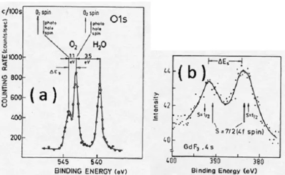
In Fig. 5, another example of the core polarization are provided. In Fig. 5(a), we give the O 1s lines from a mixture of gaseous O2 and H2O. First, we note that the energy splitting of 3.5 eV between O2 and H2O is due to the chemical shift, i.e., signifying the different chemical environment surrounding O atom between O2 and H2O. Second, interestingly, the O 1s line from O2 is split by 1.1 eV, while the O 1s line from H2O is not split. This should be understood from the core polarization. For O2, from the initial state (1s)2(2s)2(2p)4 with a total spin S=1, two possible final states could be reached as
Fig. 4. Schematic illustration of Li 1s PES of Li atom and Be 1s PES of Be atom. Li atom has the open outer shell, while Be the closed outer shell. Due to the reason, Li has two possible final states [(a) and (b)], but Be has only one possible final state [(c)]. Closed dots represent the electrons and the open dots the photoholes, respectively. Arrows signify the electron spins.
Fig. 5. (a) Oxygen 1s core-level XPS (i.e., x-ray PES) from a mixture of O2 and H2O. The figure is taken from Ref.8. (b) Gd 4s
3. 内殻分極 内殻 PES はしばしばスピンと軌道角運動量が決 まった値をもつ終状態を形成する.原子が完全な閉 殻の価電子配置を持たない限り,交換相互作用に よって内殻 PES ピークは興味深い交換分裂を示す. これが内殻分極である.図4 に Li 原子と Be 原子に おける1s 内殻 PES を模式的に示す.Li 原子に対し ては,Li(1s22s;2S)の始状態から 2 つの終状態に至る ことがすぐに分かる.
4(b) Fig. : e S Li 4(a) Fig. : e S Li S Li 3 1 2 スピン状態に依存した交換積分のために,2 つの終 状態はエネルギー的に異なる状態となり,結果とし て,1s ピークの分裂を引き起こす.一方,Be 原子の 場合,始状態 Be(1s22s2;1S)から生じる可能性がある 終状態は図4(c)に示す通りBe
2S eのみである. 図5 に内殻分極の他の例を示す.図 5(a)に O2及び H2O の混合気体からの O 1s ピークを示す.まず,化 学シフト,すなわちO2とH2O では酸素が異なる化 学的環境にあることに依存する3.5 eV のピーク分裂 が起きる.次に,興味深いことに,O2からの O 1s ピークが1.1 eV 分裂するのに対して,H2O からの O 1s ピークは分裂しないことが分かる.これは内殻分 極として理解できる.O2の場合,全スピンがS=1 で ある始状態 (1s)2(2s)2(2p)4 から 1s 軌道に存在するス ピン s=1/2 の光正孔が価電子のスピンと相互作用す る過程を経るため,次の2 種類の終状態が可能とな る.
2 3 2 1 2p 2s 1s 2p 2s 1s2 2 4 1 2 4 S S by way of the coupling of the spin s=1/2 of a photohole in 1s to the valence spin. The splitting of 1.1 eV corre-sponds to the exchange integral due to the spin coupling. On the other hand, for H2O, the initial state of O2- is (1s)2(2s)2(2p)6 with S=0, that is, the outer shell is closed, and the final state becomes (1s)1(2s)2(2p)6, i.e., S=1/2. The spin of the 1s photohole have no spin state to couple so that there is no splitting in O 1s line for H2O. The splitting of Gd 4s lines of GdF3 given in Fig. 5(b) can be also understood in the same way. The spin of the 4s photohole can couple to the spin of the final state 4f(8S
7/2), i.e., S=7/2, which gives the exchange splitting between S=3 and S=4.
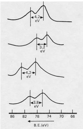
The peak splitting also varies depending on the envi-ronment of the atom concerned. Figure 6 shows the dif-ferent doublet splittings observed in the Cr 3s lines for a series of Cr compounds. This could provide chemically useful information and have an advantage compared to the chemical shift in the previous section. Comparison of the energy splitting does not require the calibration of the absolute binding energy necessary for the discussion of the chemical shift.
4. Satellites
Remembering the basic PES theory of the previous issue [1], the Fermi golden rule expression for the core-level PES includes the following transition matrix element 1 ; 1 ; , 1 dipole dipole k s N N s k b N N (1)
In Eq.(1), k is the single-electron state describing the photoelectron and N1;s is the remaining N-1 electrons in the state s, while b is the core level under consideration and b N1 the initial ground state before the PES process. dipole is the dipole operator. The photocurrent J
k, can then be expressed as
s N s N b k k J s 2 2 dipole 1; | 1 , (2)where s is the binding energy of the excited state meas-ured from the no-loss line. If N1;0 N1 , we have
only a peak from N1;0|N1 2 1 for s=0 and 0 for
s0. That is, there is no satellite. This case occurs basi-cally only in a noninteracting system, where it is said that the photohole is completely screened. On the other hand, generally, J
k, consists of the core line correspond-ing to b and its accompanying satellites according tothe number of excited states s in the PES process. It should be also noted that the present argument could be applied not only to the core line but also the valence spectra. In the following subsections, we provide some examples of rather famous satellite problems of the PES and their proper understanding.
Fig. 6. Cr 3s core-level XPS from a series of CrIII compounds
(Cr2O3, Cr3S2, CrF3, and CrCl3 from top to bottom) showing
the splitting of the 3s level. CrIII means that its oxidation state
2 3 2 1 2p 2s 1s 2p 2s 1s2 2 4 1 2 4 S S 1.1 eV の分裂はスピン相互作用による交換積分に相 当する.一方,H2O では O2-の始状態は S=0 の (1s)2(2s)2(2p)6 であり外殻が閉殻構造を持つため,終 状態はS=1/2 の(1s)1(2s)2(2p)6となる.1s 光正孔のス ピンは相互作用できる相手のスピン状態がなく,そ の結果,H2O では O 1s の分裂が起きない.図 5(b) に示したGdF3におけるGd 4s の分裂も同様の考え方 で理解できる.4s 光正孔のスピンは S=7/2 の終状態 4f(8S 7/2) と相互作用し,S=3 と S=4 の間の交換分裂 を引き起こす. このピーク分裂は結合している原子の環境にも依 存して変化する.図6 は様々な Cr 化合物からの Cr 3s ピークにおいて観測される異なった二重項分裂を示 している.これらは化学的に有効な情報をもたらし, 上述した化学シフトよりも利点が多い.エネルギー 分裂を比較する場合,化学シフトの議論で必要とな る結合エネルギーの絶対値の校正を必要としない. 4. サテライト 前回の連載で述べたPES の基本的な理論では[1], 内殻PES に対するフェルミの黄金則は次の遷移行列 要素を含む. 1 ; 1 ; , 1 dipole dipole k s N N s k b N N (1) 式(1)において,k は光電子を記述する1 電子状態, s N1; はs 状態にある残った N-1 電子,b は今考 えている内殻準位,b N1 はPES 過程が起きる前 の初期状態である基底状態である.dipoleは双極子オ ペレータである.光電流J
k, は
s N s N b k k J s 2 2 dipole 1; | 1 , (2) と与えられる.ここでsはノーロスピークから測っ た 励 起 状 態 の 結 合 エ ネ ル ギ ー で あ る . も し 1 0 ; 1 N N の 場 合 は , s=0 に 対 し て 1 1 | 0 ; 1 2 N N ,s0 に対して N1;0|N1 20 であるため,ピークは一つとなる.すなわち,サテ ライトは存在しない.このような場合は基本的に光 正孔が完全に遮蔽される相互作用しない系でのみ起 きる.一方,一般にJ
k, のスペクトルは b に相当 する内殻ピークと,これに伴って現れる励起状態 s の状態数で決まるサテライトピークで構成される. これらの議論は内殻ピークだけでなく価電子スペク トルにも適用できることを述べておく.以下では, PES における有名なサテライト問題とそれらの適切 な解釈についていくつかの例を示す.4.1. Copper dihalides
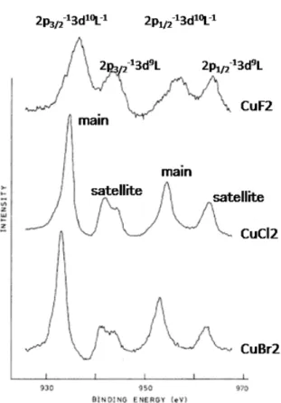
We introduce the problem of Cu 2p lines of copper dihalides like CuF2, CuCl2, and CuBr2. Firstly, the Cu 2p line is split to 2p3/2 and 2p1/2 lines due to the spin-orbit coupling. Incidentally, each of two lines (2p3/2 and 2p1/2) is further split to the main line (lower binding energy feature) and satellite (higher binding energy feature) as shown in Fig. 7. In the ground states of copper dihalides, Cu2+ has one hole in the 3d shell and the ligand shell is completely filled. This is usually written as (3d)9L, where (3d)9 refers to Cu2+ and L the outer filled shells of the halide ligands, i.e., (2p)6 for F-, (3p)6 for Cl-, and (4p)6 for Br-. A final state one may consider most imme-diately, where no valence change occurs before and after the PES, might be
3d9Lc1
3d 9Lwhere c-1 means the photohole in the core-level. Now one may ask “Does the final state of c-1(3d)9L give trivi-ally the main line?” This question or an effort to answer this question would be a starting point to understand the electronic structure of the strongly correlated electron systems like transition metal compounds.
Simply speaking, the final state of c-1(3d)9L does not give the main line for copper dihalides. Another final state, where after the core-hole creation one electron is transferred from the ligand into the d shell, leading to c-1(3d)10L-1 gives the main line, while c-1(3d)9L gives the satellite [12], as inscribed in Fig. 7. This can be under-stood by considering the additional Coulomb attraction Uc between the core hole and the 3d shell electron. A photohole on the metal ion acts as a positive charge for electrons with orbital radius larger than that of the shell on which the photohole resides. This lowers the energy of the 3d valence shell by pulling it down below the top of the ligand valence band. This picture neglects the infi-nite nature of a solid, but could be applied to open d or f shell ions with the localized nature of the orbital by Kotani and Toyozawa [13]. For a rigorous understanding, the theoretical calculation of the band structure for one-hole final state may be necessary, but it would not be easy. Instead, owing to the local nature, much simpler model with a single metal ion and the ligand cluster sur-rounding the metal ion is available. This approach using the molecular-orbital model was first taken by Asada and Sugano [14]. Similar approaches have been resorted to
thereafter by many researchers [4,12,15]. The situation can be further simplified to the two-level problem by taking both a metal ion and the ligand as single levels.
In Fig. 8, valence configurations to interpret the Cu 2p lines are given in the two-level picture. The metal ion and ligand couples to each other and makes two hybrid-ized levels. As mentioned previously, two valence con-figurations (3d)10L-1 and (3d)9L (due to the hybridization between two, it would be actually more correct to say “mostly (3d)10L-1” and “mostly (3d)9L”) are possible in the initial states. Here we importantly note that which of two would be the lowest valence configuration depends on the relative competition between Uc and E. E is the energy difference between two initial states of valence band, i.e., E=E[(3d)10L-1]-E[(3d)9L]. It is found that the copper dihalides correspond to the cases of Uc>E. More consideration of this picture can lead to the analytic analysis of Cu 2p lines [16]. Let us think of the following Hamiltonian H
Fig. 7. Cu 2p core-level XPS of CuF2, CuCl2, and CuBr2. Two
main lines split due to the spin-orbit coupling are (2p3/2)-1(3d)10L-1 and (2p1/2)-1(3d)10L-1 and their accompanying
satellites are (2p3/2)-1(3d)9L and (2p1/2)-1(3d)9L, respectively.
4.1. ハロゲン化銅
CuF2,CuCl2,CuBr2などのハロゲン化銅に見られ
るCu 2p のサテライトについて紹介する.まず Cu 2p ピークはスピン-軌道相互作用によって2p3/2と2p1/2 に分裂する.次に,二重項(2p3/2と2p1/2)はそれぞ れ,図7 に見られるように,低結合エネルギー側の 主ピークと高結合エネルギー側のサテライトにさら に分裂する.ハロゲン化銅の基底状態では,Cu2+は 3d 軌道に正孔を一つ持ち,配位子の核は完全に閉殻 となる.これは通常,(3d)9L と表される.ここで(3d)9 はCu2+を意味し,L はハロゲン配位子の満たされた 外殻,すなわち,F-の(2p)6,Cl-の(3p)6,Br-の(4p)6 を表している.PES の前後で価電子が変化しない終 状態としてすぐに考えられるのが
3d9Lc1
3d 9L である.ここでc-1は内殻の光正孔を意味する.ここ で「終状態c-1(3d)9L が主ピークを与えるのか?」と いう疑問が出てくる.この疑問に答えようとするこ とは,遷移金属化合物などの電子相関の強い系の電 子構造を理解するためのスタート地点である. 単純に言えば,終状態c-1(3d)9L はハロゲン化銅の 主ピークを与えない.図7 に示す通り,内殻に正孔 が生成された後に1 電子が配位子から d 軌道へ遷移 した終状態 c-1(3d)10L-1が主ピークを与え,c-1(3d)9L がサテライトピークとなる[12].これは内殻の正孔 と3d 殻の電子とのクーロン相互作用 Ucを考えるこ とで理解できる.金属イオンに存在する光正孔は, 光正孔が存在する殻よりも外側の軌道に存在する電 子に対して正電荷として働く.この相互作用によっ て,3d 価電子のエネルギーが配位子の最も高エネル ギーの価電子のエネルギーよりも低くなる.この説 明では,固体が無限に続くことを無視しているが, Kotani と Toyozawa によって提案された軌道が局所 化しているという特性[13]を用いて,閉殻ではない d 軌道やf 軌道イオンへ適用できる.より正確な解釈 としては,1 正孔を持つ終状態に対するバンド構造 の理論的計算が必要であるが,これは容易ではない. その代わり,局所的な振る舞いを考慮し,1 金属イ オンとそれを取り巻く配位子のクラスターで構成さ れるより単純なモデルの適用が可能である.この分 子軌道モデルを採用したアプローチは,Asada と Sugano によって最初に用いられた[14].同様のアプ ローチはその後多くの研究者によって用いられてい る[4,12,15].1 金属イオンと配位子の両方をそれぞれ 1 準位ずつとして扱うことで,系をより単純化した 2 準位問題として取り扱うこともできる. Cu 2p ピークのサテライトを説明するために図 8 に2 準位描像での価電子構造を示す.金属イオンと 配位子は相互作用し,ハイブリダイゼーションに よって 2 つの準位が形成される.上述した通り, (3d)10L-1と(3d)9L の 2 つの価電子構造(両者のハイブ リダイゼーションにより,実際には「ほぼ(3d)10L-1 とほぼ(3d)9L」と言う方がより正確)が始状態とし て可能である.ここで,どちらの価電子構造のエネ ルギーが低いかは,UcとE の競合で決まることが 重要である.E は 2 つの価電子帯の始状態のエネル ギー差E=E[(3d)10L-1]-E[(3d)9L]である.ハロゲン化 銅はUc>の系であることが分かる.これらの描像の 更なる考察により Cu 2p の解析が行える[16].次の ハミルトニアンH を考える.
a b b a
t b b a a n U c c H c a c c b (3)where c, a, and b signify the energies of Cu 2p level, (3d)9L, and (3d)10L-1, respectively, and t is the hybridiza-tion between (3d)9L, i.e.,
a and (3d)10L-1, i.e.,
b . The initial ground state 0 with nc=1 is
b c a c cos sin 0 , where
a c b
2 tan t U and
2 2 b c a b c a c 0 4 2 1 2 1 t U U E (E0 is the initial ground state energy) are noted. In the same way, the final states with nc=0 areb a sin cos 1 and b a cos sin 2 , where we note
b a
2 2 tan t and
2 2 1 b a 1 2 E E ( 1 2E are energies of two possible final states).Therefore, the binding energy separation E, that is, the distance between the main line and satellite, is
2 2
2 2 ba 4t E 4t
E
(4)
where E is given by E=b-a. Further, the peak ratio is obtained by
2 2 0 1 2 0 2 cot c c .Fig. 8. Schematic representation of valence configurations before and after the Cu 2p core-level PES in copper dihalides. Uc>E
a b b a
t b b a a n U c c H c a c c b (3) ここでc,a及びbはCu 2p 準位,(3d)9L 及び(3d)10L-1 のエネルギー,t は(3d)9L すなわち a と(3d)10L-1すな わちb の間のハイブリダイゼーションである.nc=1 の初期状態である基底状態 0 は b c a c cos sin 0 , である.ここで
a c b
2 tan t U
2 2 b c a b c a c 0 4 2 1 2 1 t U U E (E0は初期基底状態エネルギー)である.同様にnc=0 の終状態は b a sin cos 1 と b a cos sin 2 , である.ここで
b a
2 2 tan t
2 2 1 b a 1 2 E E ( 1 2 E は 2 つの可能な終状態のエネルギー)である. それゆえ,結合エネルギーの差E,すなわち主ピー クとサテライトの距離は,
2 2
2 2 b a 4t E 4t E (4) で与えられる.ここでE はE=b-aである.さらに ピークの比は
2 2 0 1 2 0 2 cot c c . で与えられる.4.2. 6 eV satellites of Ni
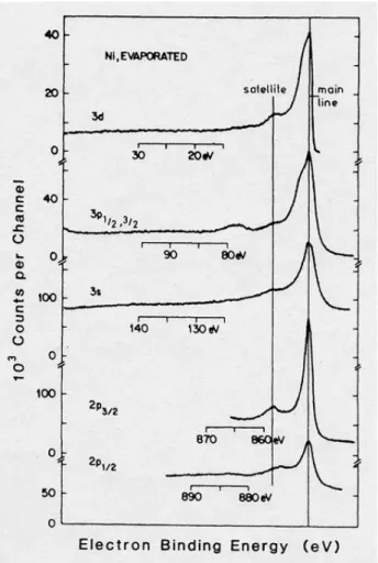
In many cases, the d or f electrons are quite localized even in metallic solids so that the previous discussion employing the atomic or cluster picture could be still valid in those metals. Of course, in insulators and semi-conductors, this statement would be valid much more strongly. In this subsection, we introduce the problem of 6 eV satellite of Ni metal [17]. Figure 9 explains the 6 eV satellite problem of Ni metal. In the figure, several core-lines and valence band spectra (3d spectra) of Ni metal are shown. It is found that each main line accom-panies a satellite at about 6 eV larger binding energy. For the understanding, the picture of Kotani and Toyozawa which was introduced in the previous subsection will be used in a similar way (see Fig.10). But, the simplified two-level model will not be employed because of the metallic bands.
Fig. 10. Schematic density of states of Ni, indicating the origin of the main and satellite for the core-level (left panel) and the va-lence level (right panel) PES. The figure is taken from Ref. 5.
Fig. 9. XPS of the 3d, 3p, 3s, 2p3/2, and 2p1/2 of Ni metal. The
main lines have been lined up to demonstrate the mostly uni-versal 6 eV satellite for each line. The figure is taken from Ref. 17.
4.2. Ni の 6 eV のサテライト 多くの場合,固体金属においてもd 及び f 電子は 局在化しているため,上述の議論で採用した原子あ るいはクラスターによる描像は他の金属に対しても 適用できる.当然,絶縁体や半導体では,この描像 はより正確なものとなる.この節では,Ni 金属に見 られる6 eV のサテライト問題について紹介する[17]. 図9 は Ni 金属における 6 eV のサテライト問題を示 している.この図は,Ni 金属のいくつかの内殻ピー クと価電子帯スペクトル(3d スペクトル)を示して いる.各主ピークが,結合エネルギーが6 eV 大きい サテライトピークを伴っていることが分かる.この サテライトを解釈するために,前節と同様にKotani と Toyozawa の描像を適用する(図 10 参照).しか しながらここでは,金属的バンドがあるために,単 純化した2 準位モデルは採用できない.
The initial state of Ni metal has (3d)9(4s)1 and two fi-nal states are possible according to two different screen-ing channels when the conduction band is pulled down below the Fermi energy (EF) by the Coulomb attraction caused by the core hole, as illustrated in the left panel of Fig. 10. First, the conduction band pulled down below EF could be filled with an additional electron and make a c-1(3d)10(4s)1 configuration. This is found to be the ground state to give the main line and called “d-screening”. Second, the screening electron could not fill the 3d band even if a localized hole is left below EF, but fill the wide 4s band, that is, “s-screening”. This makes a two-hole configuration c-1(3d)9(4s)2, which leads to the satellite. The energy of the satellite measured from the main line is E=E[(3d)9(4s)2]-E[(3d)10(4s)1]6 eV, which is approximately same for all core lines. The 6 eV satellite is also observed in the valence-band spectra (top panel of Fig. 9). In the right panel of Fig. 10, the main line corresponds to the (3d)9(4s)1 by the d-screening and the satellite to the (3d)8(4s)2 by the s-screening of the Coulomb correlation between d elec-trons. The energy separation between the main line and the satellite in this case is E=E[(3d)8(4s)2]-E[(3d)9(4s)1], which is found close to the core-level case, i.e., E[(3d)9(4s)2]-E[(3d)10(4s)1]6 eV. This is the origin of the 6 eV satellite of Ni metal.
Resonant PES (RPES) makes it possible to convinc-ingly observe the origin of the 6 eV satellite of Ni metal. In RPES, it is likely to intensify the PES signal of a par-ticular final state using the interfering resonance between the directly photoemitted electron and the Auger electron, so called the Fano resonance [18]. For Ni metal, the 3p→3d excitation can be used for a resonating channel by the photon energy corresponding to the 3p binding energy E3p (67 eV). In the case, the direct PES process leading to the valence satellite is
3d 9
3d 8 4s1e
where the kinetic energy Ek of the photoelectron is Ek=E3p-Esat and (4s)1 is a screening electron. On the other hand, the M23VV Auger process (M23VV means that the core states of 3p1/2 or 3p3/2, i.e., M23, and two valence states, i.e., VV, are incorporated) gives
3p6 3d9
3p5 3d10 Auger
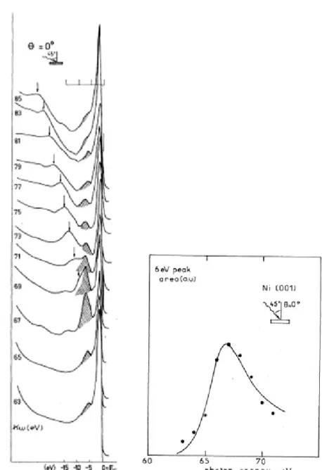
3p6 3d8 4s1ewhere the photoelectron kinetic energy is same as in the direct PES at the resonance. Two processes overlap co-herently and can give rise to an enhancement of the sig-nal of the valence satellite (3d)8(4s)1 when the photon energy sweeps through the binding energy E3p. Actual experimental results by Guillot et al. [19] are illustrated in Fig. 11.
4.3. NiO problem
NiO is a prototype material for the transition metal compounds, where the d electrons derive many of in-triguing electron correlation effects [20]. The transition metal compound is currently one of the most important research topics of the solid state physics [21]. For in-stance, the high Tc superconductors like La2CuO4, Bi2Sr2CaCu2O8, and YBa2Cu3O7, or the colossal magne-toresistance (CMR) manganese oxides like LaMnO3 still attract much active consideration.
NiO is an insulator with a gap of about 4 eV. The in-sulating nature of NiO has been a matter of controversy for a long time. In this subsection, we treat a question whether NiO is a Mott insulator or not. The Mott insula-tor [22], which will be discussed in a more systematic way in the next subsection, is a type of insulator resulting from the correlation between the d electrons and leading to a dn-1 → dn+1 transition as the lowest optical transition. A key to answer the question is the proper understanding of the valence-band PES of NiO. In Fig. 12, the XPS valence-band spectrum of NiO is provided. We need to elucidate the main line (at about 2 eV) and satellite (at about 9 eV). The initial state of NiO is (3d)8 ((3d)8 means (3d)8L, i.e., the filled ligand L could be simply omitted). For some time, it was assumed the main d-emission (i.e., main line) near the Fermi level is essentially a structure produced by a (3d)7 final state and the satellite is due to the multi-electron excitation. Along the line, it was thought that the lowest optical transition occurs like (3d)7 → (3d)9, which concluded that NiO is a Mott insulator. However, this is not correct for NiO. If one remembers the analyses of copper dihalides and Ni metal in the pre-vious subsections, one could make a correct start by as-signing the main line as (3d)8L-1 and the satellite as (3d)7. This has been checked by the RPESlike the case of the 6 eV satellite of Ni metal. Oh et al. [24] have adopted the M23VV Auger process (E3p65 eV for NiO) and made two following interfering processes
Ni 金属の始状態は(3d)9(4s)1の電子構造を持ち,図 10 の左の図で示す通り,内殻にある正孔とのクーロ ン引力によって伝導帯のエネルギーがFermi エネル ギー(EF)より低くなるとき,2 種類の異なる遮蔽 チャネルに従って2 つの終状態が可能となる.一つ 目は,EFより下がった伝導帯が他の電子によって満 たされ,c-1(3d)10(4s)1の電子配置をとるチャネルであ る.これが主ピークを与える基底状態であり,「d 遮 蔽」と呼ばれる.2 つ目のチャネルは,局在化した 正孔がEFより低い準位に残っているものの,遮蔽電 子は3d バンドを満たさず広い 4s バンドを満たす場 合で,「s 遮蔽」と呼ばれる.これは 2 正孔配置 c-1(3d)9(4s)2を形成し,サテライトが現れることにな る.主ピークから測ったサテライトのエネルギーは E=E[(3d)9(4s)2]-E[(3d)10(4s)1]6 eV となる.これは近 似的に全ての内殻ピークに対して同じとなる.6 eV のサテライトは価電子帯スペクトル(図9 の上の図) においても観測される.図10 の右の図では,主ピー クは(3d)9(4s)1の電子配置を持つd 遮蔽,サテライト は(3d)8(4s)2であるs 遮蔽に相当する.この場合の主 ピ ー ク と サ テ ラ イ ト の エ ネ ル ギ ー 間 隔 は E=E[(3d)8(4s)2]-E[(3d)9(4s)1]であり,これは内殻の場 合のE[(3d)9(4s)2]-E[(3d)10(4s)1]6 eV に近い.これが Ni 金属で見られる 6 eV のサテライトの起源である. 共鳴PES(RPES)では Ni 金属に見られる 6 eV の サテライトの起源を観測することができる.RPES では,直接放出される光電子とオージェ電子の間の 干渉共鳴,いわゆるFano 共鳴[18]を利用することで, ある終状態に起因するPES 信号の強度を増強するこ とができる.Ni 金属では,3p 結合エネルギーE3p(67 eV)に相当するエネルギーを持つ光子を用いること で,3p→3d 励起を共鳴チャネルとして利用すること ができる.この場合,価電子のサテライトに至る直 接のPES 過程は
3d 9
3d 8 4s1e で あ る . こ こ で 光 電 子 の 運 動 エ ネ ル ギ ーEk は Ek=E3p-Esatであり,(4s)1は遮蔽電子である.一方, M23VV オージェ過程(M23VV は 3p1/2あるいは3p3/2 の内殻準位すなわち M23と,2 つの価電子準位すな わちVV が関係する)は
3p6 3d9
3p5 3d10 Auger
3p6 3d8 4s1e で与えられる.ここで光電子の運動エネルギーは共 鳴する直接PES と同じである.二つの過程は可干渉 的に重なり,結合エネルギーE3pをまたいで光子のエ ネルギーを掃引すると,価電子サテライト(3d)8(4s)1 の信号が増強される.Guillot 等の実験結果[19]を図 11 に示す. 4.3. NiO 系 NiO は遷移金属化合物の基本となる材料であり,d 電子によって多くの興味深い電子相関効果が起こる [20].遷移金属化合物は現在,固体物理に関する最 も重要な研究テーマの一つである[21].例えば,La2CuO4,Bi2Sr2CaCu2O8やYBa2Cu3O7のような高温
超電導体,あるいは LaMnO3などの巨大磁気抵抗マ ンガン酸化物などが,現在でも注目を集めている. NiO はバンドギャップが 4 eV の絶縁体である. NiO の絶縁性は長年にわたって議論の対象であった. 本節では,NiO が Mott 絶縁体であるかどうかについ ての問題を取り扱う.Mott 絶縁体[22]については以 下でより系統的に述べるが,最も低エネルギーの光 学遷移であるdn-1dn+1遷移を起こすd 電子間の相関 に起因する絶縁体である.疑問に答えるための鍵は NiO の価電子帯 PES スペクトルの適切な理解である. 図12 に Ni の XPS 価電子帯スペクトルを示す.約 2 eV に存在する主ピークと約 9 eV に存在するサテラ イトを理解する必要がある.NiO の初期状態は(3d)8 である.ここで(3d)8 は(3d)8L を意味し,満たされた 配位子のL を簡単のために省略している.しばらく の間,フェルミ準位近傍のメインのd 電子放出(主 ピーク)は実質的に(3d)7 終状態によって形成され, サテライトが多電子励起によって形成されると仮定 された.これに従い,最も低エネルギーの光学遷移 は(3d)7 → (3d)9 のように起こり,NiO は Mott 絶縁体 であると結論付けられた.しかしながら,NiO につ いてこの説明は正しくない.上で述べたハロゲン化 銅とNi 金属の結果を思い出せば,主ピークを(3d)8L-1, サテライトを(3d)7 に関連付けることで正しい議論 を始められる.これは,Ni 金属の 6 eV サテライト の場合のように,RPES によって確認されている. Oh 等[24]は M23VV オージェ過程(E3p65 eV)を用 いて次の2 つの可干渉過程を調べた.
Fig. 11. Left panel: RPES of a clean Ni(100) surface for photon energy between 63 and 85 eV. The shaded structure is the 6 eV satellite and the arrows indicate the Auger transitions. Right panel: Plot of the area of the shaded structure with respect to the photon energy. The figure is taken from Ref. 19.
Fig. 12. XPS valence-band spectra of NiO. Besides the main line and oxygen bands, two structures are indicated by arrows. The figure is taken from Ref. 23.
Fig. 13. Complete band structure of NiO, combined PES and BIS. The bar diagram is from the cluster calculation. The arrows indi-cate the possible nonexcitonic optical transitions. The figure is taken from Ref. 28.
e 3d 3p 3d 3p e 3d 3p 3d 3p 3d 3p 7 6 8 6 7 6 9 5 8 6 and found the signal enhancement of the satellite corre-sponding to the final state (3d)7 in the RPES. Fujimori and Minami have analyzed the main and satellite struc-ture of NiO and drawn the same conclusion from the cluster calculation of a Ni ion with its six O neighbors [25]. A small structure (the arrowed one at about 3.5 eV) beside the main line is also found to result mainly from (3d)8L-1, but mixed with other configurations. Such mix-ing of wave functions are directly observed in the L3VV Auger spectra [26] and found to be consistent with the theoretical result. Recently, more refined reexamination of NiO is available [27]. The nonlocal screening beyond a single cluster is found to result in the Zhang-Rice (ZR) doublet bound state (i.e., roughly speaking, a new dou-blet eigenstate made from the mixing of delocalized d and p (ligand) hole states), from which the lowest energy final state near the Fermi level is proposed to be (3d)8Z-1 rather than (3d)8L-1, where Z-1 means a hole in the bound state.
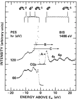
In order to discuss the optical transition across the op-tical gap, a combination of PES and the inverse PES (IPES) with the same reference point would be necessary. Combined PES and Bremsstrahlung isochromate spec-troscopy (BIS; a particular mode of doing IPES) for NiO
is given in Fig. 13. According to the figure, the lowest optical transition indicated by “A” is a (3d)8L-1 → (3d)9 (i.e., a p → d transition), corresponding to a ligand-to-metal charge transfer. This is clearly different from a (3d)7 → (3d)9 transition expected in the Mott in-sulator. Therefore, NiO is confirmed to be so called a charge-transfer insulator, not the Mott insulator. More systematic discussion of the charge-transfer insulator will be given in the next subsection.
4.4. Systematics of transition metal compounds
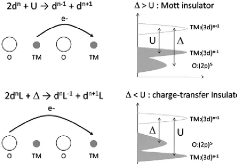
The excitation of a d electron from a transition metal ion and its transfer to another distant transition metal ion is governed by the correlation energy U (i.e., the on-site Coulomb repulsion U) between d electrons, U=E(dn+1)+ E(dn-1)-2E(dn) (see the upper left panel of Fig. 14). On the other hand, a ligand electron can also transfer to an-other distant transition metal ion. This is described by the charge-transfer energy , =E(dn+1)+ E(L-1)-E(dn)-E(L) (see the lower left panel of Fig.14). The relative size of these two energy scales determines the insulating nature of the transition metal compounds, that is, whether a Mott insulator or a charge-transfer insulator, as illus-trated in the right panel of Fig. 14. Further, we note that the optical gap transition is d → d transition (dn-1 → dn+1) for the Mott insulator, while p → d transition (dnL-1 → dn+1) for the charge-transfer insulator.
Fig. 14. Left panel: Sketch of charge transition in a transition metal compounds (TM means the transition metal and O (i.e., oxy-gen) could be replaced by other ligands). Two important parameters are defined as the electron correlation U=E(dn+1)+ E(dn-1)-2E(dn) and the charge-transfer energy =E(dn+1)+ E(L-1)-E(dn)-E(L). Right panel: Depending on the relative size of U and
e 3d 3p 3d 3p e 3d 3p 3d 3p 3d 3p 7 6 8 6 7 6 9 5 8 6 その結果,RPES における(3d)7終状態に相当するサ テ ラ イ ト の 信 号 の 増 幅 を 確 認 し た .Fujimori と Minami は NiO の主ピークとサテライト構造を解析 し,Ni イオンと 6 個の近接酸素原子からなるクラス ターに対する計算を行い,同じ結果を導いた[25]. 図中矢印で示した約3.5 eV にある主ピークの脇の小 さな構造は,主に(3d)8L-1に起因する構造であるが, 他の電子配置との混合による.このような波動関数 の混合はL3VV オージェスペクトルにおいても直接 観測され[26],理論的結果と矛盾しないことが報告 されている.最近では,NiO についてより厳密な再 検証が報告されている[27].1 クラスターのサイズを 超える非局在化した遮蔽によってZhang-Rice(ZR) 二重項結合状態(すなわち,おおまかに言うと,非 局在化した d 及び p(配位子)正孔状態に起因する 新しい二重項固有状態)が形成される.このことか ら,フェルミ準位近傍の最もエネルギーが低い終状 態が(3d)8L-1 よりもむしろ(3d)8Z-1 であることが提 案されている.ここで Z-1 は結合状態にある正孔を 意味している. 光学的ギャップ間の光学遷移を議論するために, 同じ参照準位を用いたPES と逆光電子分光(IPES)が必要である.PES と Bremsstrahlung isochromate 分 光(BIS,IPES を行うときの特別なモード)を組み 合わせてNiO に対して測定された結果を図 13 に示 す.図から,”A”で示された最低の光学遷移が(3d)8L-1 → (3d)9,すなわちp → d 遷移であり,配位子から金 属への電荷移動に相当する.これはMott 絶縁体で予 想される(3d)7 → (3d)9 遷移とは明らかに異なる.そ れゆえ,NiO はいわゆる電荷移動絶縁体であり,Mott 絶縁体ではないことが確認されている.電荷移動絶 縁体に関するより系統的な議論は以下で述べる. 4.4. 遷移金属化合物の系統性 遷移金属イオンからのd 電子の励起と他の離れた 位置に存在する遷移金属イオンへの移動は,d 電子 間の相関エネルギーU=E(dn+1)+ E(dn-1)-2E(dn),すなわ ちその場クーロン反発エネルギーU によって支配さ
れている(図14 の上左図参照).一方,配位子の電
子も他の離れた位置に存在する遷移金属イオンへ移 動することが可能である.これは電荷移動エネル ギー=E(dn+1)+ E(L-1)-E(dn)-E(L)(図 14 の下左の図を
参照)によって記述される.図14 の右に示すように これら2 つのエネルギーの相対的な大きさが,遷移 金属化合物の絶縁性,すなわちMott 絶縁体か電荷移 動絶縁体であるかを決める.さらに,光学的ギャッ プにおける遷移がMott 絶縁体では d → d 遷移(dn-1 → dn+1)であるのに対して,電荷移動絶縁体ではp → d 遷移(dnL-1 → dn+1)であることを述べておく.
Zaanen, Sawatzky, and Allen have proposed a classi-fication scheme of the transition metal compounds (i.e., the 3d-valence insulator) based on the relative size of U and [29]. In Fig. 15, the simple diagram of the Zaan-Sawatzky-Allen scheme is represented, where various insulating (also metallic) natures found among transition metal compounds could be understood. For U < , the transition metal compound is the Mott insulator whose gap is scaled by U. On the other hand, for U > , the insulator is the charge-transfer type with its gap scaled by . The on-site repulsion U depends strongly on the kind of transition metal, while the charge-transfer energy depends on the kind of ligand, i.e., the electro-negativity of the ligand (electroelectro-negativity is the tendency to attract electrons towards itself in a covalent bond). The difference in Madelung potential between the transition metal and ligand also influences (Madelung potential is the electrostatic potential of a single ion in a crystal). More detailed works would be necessary to reveal the competition between two. However, it is known that the on-site repulsion U decreases in going from Cu2+((3d)9) to Ti3+((3d)1). This means that the transition metal oxides with the element at the beginning of the 3d series like Ti, V, and Cr would tend to be the Mott insulators. In those systems, the final state to which the feature near the Fermi level is attributed in the valence-band PES spectra would correspond to (3d)n → (3d)n-1 without any partici-pation of the ligand, differently from NiO in the previous subsection. As a matter of fact, according to the extended
PES studies, TiO and Cr2O3 are found to be the Mott insulator and Ti2O3 and V2O3 the Mott compound (not actually insulators, but metals; signifying the generalized Mott-type electronic structure near the Fermi level). On the other hand, NiO, CuO, and high Tc superconducting materials are found to be typical charge-transfer insula-tors. The boundary between two types of insulators is not always sharp. In FeF2, the two final states ((3d)5 and (3d)6L-1) are strongly mixed and thus the above classifi-cation could not be applied [30].
5. Summary
We have overviewed the final states of the material after the PES process and the satellites of PES as the final-state-effects, especially when such final states are made from the local (atomic-like or cluster-like) excita-tions. This topic frequently includes the transition metal compounds because the fundamental excitation in those systems is basically local due to the strong electron cor-relation. The transition metal compound might be actu-ally one of the most important issues in the materials science. We have briefly introduced a few famous and prototypical problems related to the satellites of PES of such transition metal compounds.
6. Acknowledgment
We acknowledge Prof. Goro Mizutani for encouraging this review work on the photoemission electron spec-troscopy. We also acknowledge Dr. SangWook Han and Dr. Yukiko Yamada-Takamura for reading the manuscript. This work was supported by Special Coordination Funds for Promoting Science and Technology from MEXT, Japan.
7. References
[1] J. D. Lee, J. Surf. Anal. 16, 42 (2009). [2] T. Koopmans, Physica 1, 104 (1933).
[3] P. Thiry, D. Chandesris, J. Lecante, G. Guillot, P. Pinchaux, and Y. Petroff, Phys. Rev. Lett. 43, 82 (1979).
[4] Core-level spectroscopy in condensed systems, ed. by J. Kanamori and A. Kotani (Springer-Verlag, 1988). [5] S. Hüfner, Photoelectron spectroscopy
(Springer-Verlag, 2003).
[6] G. D. Mahan, Many-particle physics (Kluwer Aca-demic/ Plenum Publishers, 2000).
Fig. 15. Diagram of Zaanen-Sawatzky-Allen scheme for classi-fication of transition metal compounds based on the relative size of U and . wd and wp are the bandwidths of d- and