Japan Advanced Institute of Science and Technology
JAIST Repository
https://dspace.jaist.ac.jp/Title
Structural and electronic properties of Ce@C_<82>
Author(s)
Shibata, K; Rikiishi, Y; Hosokawa, T; Haruyama,
Y; Kubozono, Y; Kashino, S; Uruga, T; Fujiwara,
A; Kitagawa, H; Takano, T; Iwasa, Y
Citation
Physical Review B, 68(9): 094104-1-094104-7
Issue Date
2003-09
Type
Journal Article
Text version
publisher
URL
http://hdl.handle.net/10119/3365
Rights
K. Shibata, Y. Rikiishi, T. Hosokawa, Y.
Haruyama, Y. Kubozono, S. Kashino, T. Uruga, A.
Fujiwara, H. Kitagawa, Takano and Y. Iwasa,
Physical Review B, 68(9), 094104, 2003.
"Copyright 2003 by the American Physical
Society."
http://prola.aps.org/abstract/PRB/v68/i9/e094104
Description
Structural and electronic properties of Ce@C
82K. Shibata,1Y. Rikiishi,1T. Hosokawa,1Y. Haruyama,1Y. Kubozono,1,2,3,*S. Kashino,1T. Uruga,4A. Fujiwara,3,5 H. Kitagawa,6,7,†T. Takano,8and Y. Iwasa3,8
1Department of Chemistry, Okayama University, Okayama 700-8530, Japan
2Center for Molecular-Scale Nanoscience, Institute for Molecular Science, Okazaki 444-8585, Japan 3CREST, Japan Science and Technology Corporation, Kawaguchi 332-0012, Japan
4Japan Synchrotron Radiation Research Institute, Sayo 679-5198, Japan 5Japan Advanced Institute of Science and Technology, Ishikawa 923-1292, Japan
6Department of Chemistry, University of Tsukuba, Ibaraki 305-8571, Japan 7PRESTO, Japan Science and Technology Corporation, Kawaguchi 332-0012, Japan
8Institute for Materials Research, Tohoku University, Sendai 980-8577, Japan
共Received 5 February 2003; revised manuscript received 19 May 2003; published 4 September 2003兲
X-ray diffraction patterns for a solid sample of Ce@C82that contains a mixture of two isomers, I and II, can
be indexed in a face-centered cubic lattice with a lattice constant of 15.88共5兲 Å, while x-ray diffraction patterns for Ce@C82 isomer I alone indicate a simple cubic lattice with a lattice constant of 15.78共1兲 Å. Rietveld
refinement for the x-ray diffraction pattern of the latter, Ce@C82isomer I, has been carried out with a space
group of Pa3¯ . Thin films of Ce@C82 were first prepared by thermal deposition under ⬃10⫺7 Torr. The
Raman spectra for these thin films show a peak ascribable to a Ce-C82cage-stretching mode at⬃160 cm⫺1,
implying that the valence of Ce in this structure is ⫹3. This valence of ⫹3 is supported by Ce LIII-edge XANES for a thin film of Ce@C82. Furthermore, the local structure around the Ce ion could be determined by
Ce LIII-edge EXAFS for a thin-film. Transport properties of a thin film of Ce@C82have been studied by a
four-probe method, and these demonstrate a semiconducting behavior with a small gap of 0.4 eV.
DOI: 10.1103/PhysRevB.68.094104 PACS number共s兲: 61.48.⫹c, 81.05.Tp
I. INTRODUCTION
Much effort has been directed towards a clarification of the valence of metal ions encapsulated in metallo-fullerenes and any electron transfer from these metal ions to the fullerene cages. This is necessary because the valence of metal ions and the charge on the fullerene cages play impor-tant roles in the physical properties of fullerenes.1 The va-lence of such metal ions has been studied by ESR, UPS, x-ray diffraction, XPS, and XANES.2– 6 The studies were first performed for La@C82 because La@C82 is the most fundamental of the lanthanide ion endohedral fullerenes. The ESR spectrum of La@C82 suggested that the valence of La
in La@C82was not⫹2 but ⫹3, based on the fact that eight
hyperfine lines were observed with a small hyperfine cou-pling 共hfc兲 constant, 1.2 G, due to the hfc of an unpaired electron to a 139La ion (I⫽7/2).2UPS also showed that the valence of La in La@C82was⫹3, based on the fact that the
two components at 1.6 and 0.9 eV in the difference spectrum between La@C82 and C82 were observed with an intensity ratio of 2:1.3An analysis of the x-ray diffraction pattern by the maximum entropy method suggested a valence of⫹3 for La in [email protected] XPS profile for La@C82was similar to
that of La2O3,5 indicating that the valence of La was⫹3.6 Studies to estimate the valence of metal ions are gradually being applied to other metallofullerenes.
The electronic structure near the Fermi level in the solid state physics and chemistry of metallofullerenes is very im-portant. The onset of the UPS spectrum was observed at 0.35 eV for La@C82, indicating that the gap of at least 0.35 eV
has been opened.6Very recently, Nuttall et al. found an
op-tical gap of 0.3 eV for La@C82 based on its UV-VIS-NIR
spectrum;7 this spectrum is consistent with the results of EELS.8Transport measurements were performed on a single crystal of La@C82by the two-probe method. They showed a
semiconducting behavior with an Eg of 0.3 eV.9 Subse-quently all experimental results showed Eg⬃0.3 eV for
La@C82. Very recently we studied the transport properties
of thin films of Dy@C82. These studies demonstrated a
semiconducting behavior for Dy@C82 with an Eg of 0.2
eV.10
Information on the electronic properties of many metal-lofullerenes is urgently needed because present information is insufficient for use in promoting the solid state physics and the materials science based on metallofullerenes as well as their application to electronic devices. In the present study, we have selected Ce@C82as a target for clarification of the
structure and electronic properties because Ce is an element adjacent to La in the Periodic Table. The electronic configu-ration of the Ce atom is关Xe兴关4 f2兴关6s2兴. Thus Ce possesses 4 f electrons. The coexistence of 4f electron共s兲 on Ce and electrons on the C82 cage in Ce@C82 may provide new
in-formation on the physics and chemistry of bifunctional mo-lecular systems based on a coupling of the localized spin with conduction electrons.
The existence of two types of crystal structures in isomer-mixture samples of Ce@C82has been demonstrated by x-ray
diffraction patterns.11One, for the sample sublimed at 873 K, is a face-centered-cubic共fcc兲 structure 共space group Fm3¯m) and the other, for the sample dried at 532 K, is a hexagonal close packed共hcp兲 structure 共space group P63/mmc). In the
dried at 623 K has been studied by x-ray powder diffraction because the sample dried at this temperature was used to form a thin film of Ce@C82. Furthermore, the x-ray
diffrac-tion patterns for the isomer-separated samples of Ce@C82
have been studied with synchrotron radiation, and a Rietveld refinement has been carried out for the major isomer. The Raman, XANES, and transport properties of thin films of Ce@C82have been studied in order to clarify the electronic
structures.
II. EXPERIMENT
A Ce@C82 sample was obtained by the same procedure
used to obtain Dy@C82. 10,12
Samples were characterized by time-of-flight mass and UV-VIS-NIR absorption spectra. The quantity and purity of Ce@C82 obtained were ⬃3 mg and
⬃99.5%, respectively. A solid sample of Ce@C82 was
ob-tained by evaporating toluene from a toluene solution of pu-rified Ce@C82under reduced pressure at 293 K. This result-ing sample contained two isomers with a molar ratio of 4:1; the major and minor isomers were designated I and II, re-spectively, as for Dy@C82,10,12and the names I and II
cor-respond to the order of retention times during high perfor-mance liquid chromatography共HPLC兲. The isomer-separated samples, isomers I and II, were obtained by repeating the HPLC three times; the quantity and purity of the isomer I were⬃1 mg and over 99%, respectively, while those of iso-mer II were ⬃0.3 mg and ⬃99%, respectively. Solid samples of isomers I and II were also obtained by evaporat-ing toluene from their toluene solutions. A trace of toluene was removed from the Ce@C82solid sample containing two
isomers 共isomers-mixture兲 and from the solid samples of Ce@C82 isomers I and II by a dynamical pumping under a
pressure of 10⫺5Torr at 373 K for 5 h, at 473 K for 12 h, and then at 623 K for 49 h. These dried samples, ready for x-ray diffraction and Raman measurements, were introduced into glass capillaries (⫽0.5 mm) without any exposure to air in an Ar glove box. The x-ray powder diffraction pattern for the sample of Ce@C82isomers-mixture was measured at
295 K with Cu K␣ radiation (⫽1.5418 Å, 40 kV, and 200 mA兲 by a Rigaku Rint 1500 x-ray diffractometer. The x-ray diffraction patterns for Ce@C82 isomers I and II were
mea-sured at 295 K, with a synchrotron radiation of ⫽0.7997(4) Å at BL-1B of KEK-PF, Japan. The Rietveld refinement for the x-ray diffraction pattern for isomer I was achieved with the Rietan-2000 program developed by Izumi.13
A Ce@C82 thin film was fabricated according to the
fol-lowing procedure. A highly doped n-type Si共100兲 wafer was immersed in a diluted HF solution in order to remove any native oxide.14A SiO2 layer was grown on the Si wafer by
dry oxidation at 1273 K for 6 h. The thickness, t, of the SiO2 layer was determined by an ellipsometer to be 3100 Å. The SiO2/Si substrate was washed with acetone, methanol, and
purified water by ultrasonic irradiation prior to fabrication of electrodes and fullerene thin film. The four electrodes for the resistivity measurement,, were formed on the SiO2/Si
sub-strate by a thermal deposition of gold through a shadow mask under a vacuum of⬃10⫺7Torr; the channel length, L,
was 20m. The t of electrodes was estimated to be 500 Å by a quartz-crystal oscillator. The Ce@C82 isomers-mixture
was deposited on the substrates under the same pressure of 10⫺7 Torr. This thin film then contained isomers I and II with a molar ratio of 4:1. The deposition rate was regulated below 1 Å s⫺1. The t of Ce@C82 thin-film was determined
by a surface profiler to be 4700 Å, and the width of the thin film was 5000 m.
The Raman spectra for crystalline Ce@C82isomers I and II, and a Ce@C82thin film were measured at an excitation of
632.8 nm by a He-Ne laser with an NR-1000 system共JEOL兲 for frequency 共兲 region of 100– 850 cm⫺1. The Ce LIII-edge XANES and EXAFS for the Ce@C82 thin film
were measured by fluorescence and electron yield detection, respectively, with synchrotron radiation at BL01B1 of SPring-8, Japan. The EXAFS of Ce@C82thin film was
ana-lyzed with XAFS93 and RBF93 programs developed by Maeda.15
III. RESULTS AND DISCUSSION A. Structure of Ce@C82
The UV-VIS-NIR spectra of Ce@C82isomers I and II are shown in Figs. 1共a兲 and 1共b兲. Two peaks are observed at 632 and 1008 nm for isomer I, while they lie at 710 and 1070 nm for isomer II. The peaks for the isomer I show a blueshift by 60– 80 nm in comparison with those for the isomer II. Peaks for isomers I of La@C82, Pr@C82, and Dy@C82, which
have a C2v symmetry shifted to blue by 60–100 nm when
compared with those of isomers II which have Cs
symmetry.16 –19The wavelength of 632 nm for the first peak of Ce@C82 isomer I is close to those for isomers I (C2v) of FIG. 1. UV-VIS-NIR absorption spectra for Ce@C82isomers共a兲 I and共b兲 II.
K. SHIBATA et al. PHYSICAL REVIEW B 68, 094104 共2003兲
La@C82共620 nm兲, Pr@C82共640 nm兲 and Dy@C82共632 nm兲
reported previously, while the wavelength of 710 nm for Ce@C82 isomer II is close to those for isomers II (Cs) of
La@C82 共705 nm兲, Pr@C82 共710 nm兲 and Dy@C82 共694
nm兲. These results show that the symmetries of Ce@C82
iso-mers I and II are C2vand Cs, respectively. Therefore the C82
cages in isomers I and II should have these same symmetries. The x-ray diffraction pattern for the dried sample of Ce@C82isomers-mixture can be indexed in a fcc lattice with
a of 15.88共5兲 Å. This diffraction pattern is consistent with that of the sublimed Ce@C82 sample reported by Nuttall et al.; it was attributed to the fcc structure with a ⫽15.766 Å.11 Consequently, crystals of the Ce@C
82
isomers-mixture dried at 623 K under a vacuum of 10⫺5 Torr have a fcc structure as in the sublimed sample. In the present study, the dried sample is used to form the thin film by the thermal deposition. The x-ray diffraction pattern of Ce@C82isomer I is shown in Fig. 2共a兲; it can be indexed
with an sc lattice. This pattern is similar to that of Dy@C82 isomer I. In the Rietveld refinement, the space group for crystals of Ce@C82isomer I was assumed to be Pa3¯ as for the Dy@C82isomer I reported recently by our group.
10
For a C2v-Ce@C82 molecule 共isomer I兲 an orientational disorder
around关111兴 was assumed, because the symmetry is required for the space group Pa3¯ . The center of the C82 cage was
placed on the origin of the unit cell, and the C2 axis of the
C82 cage was aligned along关111兴. The number of
crystallo-graphically independent C atoms is 82 in the Pa3¯ unit cell because the C2v-C82 cage has no 3¯ symmetry. All C atoms occupy the 24d site with an occupancy factor of 1/6. The Ce atom occupies the 8c site with an occupancy factor of 1/2; the Ce ion lies on the C2 axis to satisfy the C2vsymmetry in
the Ce@C82molecule. The rotation anglewas fixed to 30°
as in the case of the Dy@C82isomer I, where the definition
offollowed that in Dy@C82isomer I.10The coordinates of
x, y , and z for the C82 cage were fixed to the initial ones
with CuC bond lengths of 1.37–1.47 Å; the initial coordi-nates were the same as those used in the Rietveld analysis of Dy@C82.
20
The x-ray diffraction pattern of Ce@C82isomer I and that
calculated with the structural parameters determined from the Rietveld refinement are shown in Fig. 2共b兲. The final Rwp
and integrated intensity R factor, RI, were 0.027 and 0.102,
respectively. The Ce@C82 molecule viewed along 关111兴 is
shown in the inset of Fig. 2共b兲. The a value for Ce@C82
isomer I was determined to be 15.78共1兲 Å, which is the same as that, 15.78共1兲 Å, for Dy@C82 isomer I.10 The B of C
atoms is 7(2) Å2, while that of Ce atom, 132(35) Å2, is very large as for that of Dy in the Dy@C82isomer I.
From this analysis, it appears that the Ce@C82 molecule
takes part in a ratchet-type disorder to satisfy the 3¯ symme-try, and the Ce ion exhibits considerable disorder within the C82 cage. When Rietveld analyses were performed by
vary-ing the distance between the Ce atom and the C82cage center
in Ce@C82, the Rwpshowed an almost flat minimum within
⫾2.2 Å from the cage center. The Rwp value was slightly
high near the cage center. This result implies that the Ce in Ce@C82has considerable freedom of motion within the C82
cage. Recently, a flat Rwp minimum was also found in the
Rietveld analyses of Dy@C82. 21
Further, considerable mo-tion of La was observed in La@C82 isomer I by the MEM
analysis.4 These results also support the floating motion of Ce in Ce@C82.
The x-ray powder diffraction pattern for Ce@C82 isomer
II was indexed with an sc lattice of a⫽15.6(1) Å. However, the x-ray diffraction data obtained were very poor because only small amounts of the sample,⬃0.3 mg, were available. Consequently, a Rietveld analysis could not be done satisfac-torily for Ce@C82isomer II.
B. Vibrational modes of Ce@C82
The Raman spectra for powder samples of Ce@C82 iso-mers I and II are shown in Figs. 3共a兲 and 3共b兲, respectively. A peak for the Ce cage stretching mode in Ce@C82isomer I
is observed at⫽160 cm⫺1, while that for isomer II is ob-served at ⫽163 cm⫺1. The Raman spectrum for the Ce@C82thin film is almost the same as that for the crystal-line sample of Ce@C82 isomer I. The peak for the Ce-C82
stretching mode in the Ce@C82 thin film is observed at ⫽160 cm⫺1. The observation of a stretching mode at the
same value as that for the Ce@C82 isomer I shows that the
thin film is not damaged by the thermal deposition and mainly consists of Ce@C82isomer I. The result is consistent FIG. 2. 共a兲 Observed x-ray diffraction pattern for Ce@C82
iso-mer I, and共b兲 the observed x-ray diffraction pattern (⫹ symbols兲 and that calculated with the structural parameters determined by Rietveld refinement 共solid line兲. In 共a兲 the symbols 䊉 show those peaks that cannot be indexed by a fcc lattice. In 共b兲 the allowed peak positions and the difference between the observed and calcu-lated patterns are drawn by a check mark共middle兲 and a solid line
共bottom兲, respectively. The peak indicated by an asterisk did not
appear in the calculated pattern. This peak was attributed to effects of the sample holder. A molecule of Ce@C82isomer I viewed along
the 关111兴 direction is shown in the inset of 共b兲. Black and white balls refer to the Ce and C atoms, repectively.
with the fact that the isomers-mixture contains the isomers I and II with the molar ratio of 4:1.
The values for the stretching mode of Ce@C82 are similar to those for the isomers-mixture of La@C82
(162/163 cm⫺1), Gd@C82 (152/155 cm⫺1), and Ce@C82
(156/162 cm⫺1) reported previously,22,23 in which the va-lence of metal ions is reported to be⫹3.1On the other hand, the peaks for the stretching mode of the metal cage in isomer III (C2 symmetry兲 of Tm@C82 and Sm@C82, and the isomers-mixture of Eu@C74 are observed around
120 cm⫺1;22in these the valence of the metal atom is⫹2.1 The peaks for the stretching mode for both isomers of Ce@C82clearly show that the valence of Ce is⫹3.
The values of three La-C82 modes calculated
theoreti-cally for C2v-La@C82 were 159, 27, and 30 cm⫺1 for the A1, B1, and B2modes, respectively.24The A1mode refers to
the stretching vibration mode, while the B1 and B2 modes
refer to lateral vibrational modes. The value of observed for the Ce@C82 isomer I is consistent with a theoretical
value for the A1mode for C2v-La@C82. 24
This indicates that the difference between the encapsulated metal ions in La@C82and Ce@C82does not affect thevalue for the A1
stretching modes if the cage structures and the valences of the metal ions are the same in each.
Further, the difference in cage symmetry between Ce@C82 isomers I and II causes a slight shift from 160 to
163 cm⫺1 in thefor the A1 stretching mode, as shown in
Figs. 3共a兲 and 3共b兲. This shift is much smaller than that caused by the difference in the valence of the metal ion; the theoretical value of for Cs-La@C82 was almost the same as that for [email protected] Peaks for the radial breathing
mode are observed at the same value of , 430 cm⫺1 for Ce@C82isomers I and II. Other peaks are observed at values
of similar in Ce@C82isomers I and II.
C. Valence of Ce in Ce@C82determined by XANES
The Ce LIII-edge XANES spectra of Ce@C82 thin-film
and CeO2 powder are shown in Fig. 4. The threshold
ener-gies, E0, of the Ce LIII-edge XANES spectra are 5721 and 5724 eV for Ce@C82and CeO2, respectively. A single peak
is observed for Ce@C82, while the XANES spectrum of CeO2 is more complex. The XANES spectrum for CeO2 is
consistent with that reported previously.26 The E0 value for Ce@C82 shifts by 3 eV to lower energy than that for CeO2
with the valence of⫹4.
We previously reported that the E0 value from Eu
LIII-edge XANES for Eu@C60shifted to a lower energy by 6
eV compared with that for Eu2O3, and that the E0 value for
Eu@C60was close to that for EuS.27The results implied that
the valence of Eu in Eu@C60was not⫹3 but ⫹2 as in EuS.
Furthermore, the E0 value of Tm@C82is shifted to a lower
energy by 7 eV than that of Tm2@C82. 28
Therefore Kikuchi et al. concluded that the valences of Tm@C82and Tm2@C82
were⫹2 and ⫹3, respectively. The shift in the value of E0 to a lower energy in Ce@C82suggests that the valence of Ce
in Ce@C82 is different from that in CeO2. However, the shift value of E0, 3 eV, is smaller than that caused by the
change of the valence from⫹2 to ⫹3.
According to Ref. 26, the two peaks denoted as C and D in the XANES spectrum of CeO2 are assigned to LIII (2 p
→5d) transitions screened by localized 4 f and the extended
4 f states, respectively. The shoulders denoted as A and B are assigned to shakedown satellites of peaks C and D. A XANES spectrum similar to that for CeO2 is observed for
TbO2 and PrO2with the valence of⫹4, while shoulder B is
found to be coincident with the single line observed for the corresponding trivalent oxides and trivalent compounds.26 The single line in the XANES for Ce@C82is consistent with
a shoulder B for CeO2, as seen from Fig. 4. This result shows that the valence of Ce in Ce@C82is⫹3.
D. Local structure of Ce@C82
The radial distribution function, ⌽(r), obtained by the Fourier transform of the Ce LIII-edge EXAFS oscillation, (k), in the k-region of 2.0– 10.0 Å⫺1 for a thin film of Ce@C82is shown in Fig. 5共a兲. Two pronounced peaks in the
absolute portion of ⌽(r) are observed at 1.82 and 2.48 Å. The peaks can be assigned to scattering between Ce and the first nearest C atoms, C共1兲, and that between Ce and the second nearest C atoms, C共2兲. The peaks in ⌽(r) are
ob-FIG. 3. Raman spectra for the crystalline Ce@C82isomers共a兲 I and共b兲 II in the region of 100– 800 cm⫺1.
FIG. 4. Ce LIII-edge XANES spectra for a thin film of Ce@C82 and for a CeO2powder.
K. SHIBATA et al. PHYSICAL REVIEW B 68, 094104 共2003兲
served at r values that are smaller than the real distances because the Fourier transform is performed without consid-eration of the phase shift of absorbing and scattering atoms. The structural parameters of Ce-C共1兲 and Ce-C共2兲 were determined by a least-squares fitting 共two-shell fitting兲 for
(k) 关Fig. 5共b兲兴 obtained by an inverse-Fourier transform of ⌽(r) in the r region of 1.32–3.05 Å. The FEFF code was used for the phase shifts of absorbing and scattering atoms, and the backscattering amplitudes of the scattering atoms.29 The coordination numbers, N, for C共1兲 and C共2兲 were fixed to 6 by assuming that the Ce ion lies along the C2axis on the
six-membered ring of the C82 cage with C2vsymmetry.
Al-though this sample contains two isomers of I and II, the fraction of isomer I with the C2vsymmetry is found from the HPLC profile to be larger than 80%. The distance of Ce-C共1兲, rCe-C(1) and the mean-square displacement,共1兲, were
determined to be 2.473共9兲 Å and 0.005(1) Å2, respectively, while the distance of Ce-C共2兲, rCe-C(2), and the mean-square
displacement, 共2兲, were determined to be 2.743共9兲 Å and 0.0026(9) Å2, respectively. The (k) calculated with the structural parameters described above is shown in Fig. 5共b兲, together with the experimental (k); the final R factor was 0.084.
The rCe-C(1) is consistent with those determined for the
powder samples of Dy@C82关2.48共2兲 Å兴, Gd@C82 isomer I 关2.56共1兲 Å兴, and La@C82 isomer I 关2.47共2兲 Å兴 by
EXAFS.16,30,31On the other hand, rCe-C(2)is slightly smaller than those for Dy@C82 关2.83共2兲 Å兴, Gd@C82 isomer I
关2.77共3兲 Å兴, and La@C82 isomer I 关2.94共7兲 Å兴.16,30,31 The
structural parameters obtained from EXAFS show that the Ce@C82 molecule is not damaged by thermal deposition
when a thin film is formed; this finding is also supported by the Raman spectra as described in Sec. III B.
E. Transport property of Ce@C82
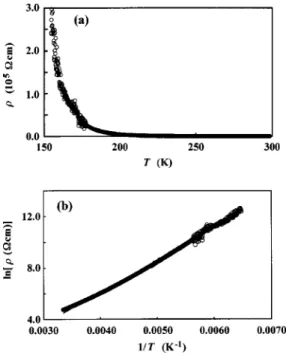
The temperature dependence offor a Ce@C82thin film
is shown in Fig. 6共a兲. Thevalue decreases with an increase in temperature up to 300 K. Thevalue is 130⍀ cm at 290 K. The lnvs 1/T plots from 155 to 290 K are shown in Fig. 6共b兲; they exhibit a linear relationship. This implies that Ce@C82is a normal semiconductor. The value of Egis
esti-mated to be 0.4 eV; this is smaller than those of C60 共1.8 or
2.1 eV兲 and C70 共2.2 eV兲. 32–34
The Eg value of Ce@C82 is
slightly larger than those of La@C82and Dy@C82which are
estimated from the temperature dependence of共Refs. 9 and 10兲 to be 0.3 and 0.2 eV, respectively, These results show that M @C82( M : La, Dy and Ce兲 is a semiconductor with a
small value of Eg. The small Egof Ce@C82may lead to the
appearance of novel physical properties. For example, the semiconductor-metal transition may be observed by applica-tion of pressure because the value of Eg is expected to de-crease owing to an inde-crease in the bandwidths of conduction and valence bands caused by an increase in the hopping in-tegral. No anomaly in the plots of vs T is observed at 150–300 K. Very recently, the photoelectron emissions for thin films of Dy@C82 and Ce@C82 have been studied, and
the Eg values are suggested to be 0.2 and 0.3 eV, respectively.35 These Eg values are consistent with that
de-termined from thevs T plots in the present study.
IV. CONCLUSION
Crystalline samples of Ce@C82 isomers I and II were
obtained, and the structure of isomer I was determined to be
FIG. 5. 共a兲 ⌽共r兲 obtained from the Ce LIII-edge EXAFS for a Ce@C82thin film.共b兲 The experimental(k) 共• symbols兲 for Ce-C共1兲 and Ce-C共2兲, and(k) 共solid line兲 calculated with the struc-tural parameters determined by an EXAFS data analysis. In共a兲 the thin and thick lines refer to the imaginary and absolute components of⌽(r), respectively.
FIG. 6. 共a兲 vs T and 共b兲 ln vs 1/T plots for a thin film of Ce@C82. In 共b兲, the solid line refers to that fitted with a linear relationship.
sc ( Pa3¯ ) with a⫽15.78(1) Å. The Rietveld refinement of the x-ray powder diffraction data for Ce@C82 isomer I has been achieved by the adoption of C2v-symmetry for the
mol-ecule. The C2 axis of Ce@C82 isomer I is aligned along
关111兴, and the molecule is orientationally disordered to sat-isfy the 3¯ symmetry.
Thin films of Ce@C82 were prepared by thermal
deposi-tion of a pure sample. The Ce LIII-edge EXAFS for thin films
of Ce@C82 showed that no thermal damage had occurred.
This implies that thin films of metallofullerenes can be pre-pared by thermal deposition without damage. This result will open doors to studies of the physical properties of the thin films of metallofullerenes and applications to electronic de-vices such as field-effect transistors 共FET’s兲. Very recently, we succeeded in fabricating a FET with a thin film of Dy@C82that operated as an n-channel normally on a FET.36 The valence of Ce in Ce@C82 has been found to be⫹3,
on the basis of the Raman spectra and Ce LIII-edge XANES
for a thin film of Ce@C82. The Raman spectra for the
Ce@C82isomers I and II have been studied, and a slight shift
of 3 cm⫺1was observed in the peak for the Ce-cage stretch-ing mode between isomers I and II. The shift is much smaller than that, ⬃40 cm⫺1, caused by a difference in the valence of the metal ion. This implies that the force constant of the metal cage, which is directly related to the bond strength between the metal ion and the C82 cage, is dominated by an
ionic interaction.
The -T plots of a thin film of Ce@C82 showed that
Ce@C82is a normal semiconductor with an Egvalue of 0.4
eV. The electronic configuration of Ce@C82 can be ex-pressed as关Ce兴3⫹关C82兴3⫺because the valence of Ce is⫹3.
This makes one anticipate the coexistence of a localized 4 f electron on the Ce ion and a delocalized conduction band originating from C82
3⫺
. Actually, Ce@C82showed no metallic
behavior. Nevertheless, the small Eg value may result in a
semiconductor-metal transition on application of pressure to Ce@C82. Therefore some interesting physical properties
caused by the coexistence of a localized 4 f electron and a conduction electron may be found for Ce@C82.
ACKNOWLEDGMENTS
The authors thank Dr. Masafumi Ata and Mr. Koji Ka-dono of SONY Coorporation for their valuable suggestions concerning the electronic structure of Ce@C82, and Dr.
Kaoru Kobayashi and Professor Shigeru Nagase of the Insti-tute for Molecular Science for their valuable suggestions concerning the vibrational modes of Ce@C82isomers. They
thank Takayoshi Kanbara and Yasuhiro Takabayashi for their helpful assistance through this work. The x-ray diffraction study was performed under the KEK-PF Proposal No. 2002G201, and the XAFS study was performed under the Spring-8 proposal 2002B0547-NX-np. This work was sup-ported by CREST of Japan Science and Technology Corpo-ration and by the Special Research Project and Joint Studies Program共2001–2002兲 of the Institute for Molecular Science.
*Email address: [email protected]
†Present address: Department of Chemistry, Kyushu University,
Fukuoka 812-8581, Japan.
1See, for example, H. Shinohara, Rep. Prog. Phys. 63, 843共2000兲;
M. Knupfer, Surf. Sci. Rep. 42, 1共2001兲.
2R. D. Johnson, M. S. de Vries, J. Salem, D. S. Bethune, and C. S.
Yannoni, Nature共London兲 355, 239 共1992兲.
3S. Hino, H. Takahashi, K. Iwasaki, K. Matsumoto, T. Miyazaki,
S. Hasegawa, K. Kikuchi, and Y. Achiba, Phys. Rev. Lett. 71, 4261共1993兲.
4E. Nishibori, M. Takata, M. Sakata, H. Tanaka, M. Hasegawa, and
H. Shinohara, Chem. Phys. Lett. 330, 497共2000兲.
5J. H. Weaver, Y. Chai, G. H. Kroll, C. Jin, T. R. Ohno, R. E.
Haufler, T. Guo, J. M. Alford, J. Conceicao, L. P. F. Chibante, A. Jain, G. Palmer, and R. E. Smalley, Chem. Phys. Lett. 190, 460
共1992兲.
6D. M. Poirier, M. Knupfer, J. H. Weaver, W. Andreoni, K.
Laa-sonen, M. Parrinello, D. S. Bethune, K. Kikuchi, and Y. Achiba, Phys. Rev. B 49, 17 403共1994兲.
7C. J. Nuttall, Y. Hayashi, K. Yamazaki, T. Mitani, and Y. Iwasa,
Adv. Mater.共Weinheim, Ger.兲 14, 293 共2002兲.
8K. Iizumi, Y. Uchino, K. Ueno, A. Koma, K. Saiki, Y. Inada, K.
Nagai, Y. Iwasa, and T. Mitani, Phys. Rev. B 62, 8281共2000兲.
9K. Honkura, K. Ishii, T. Watanuki, A. Fujiwara, and H. Suematsu 共private communication兲.
10Y. Kubozono, Y. Takabayashi, K. Shibata, T. Kanbara, S. Fujiki,
S. Kashino, A. Fujiwara, and S. Emura, Phys. Rev. B 67, 115410
共2003兲.
11C. J. Nuttall, Y. Inada, Y. Watanabe, K. Nagai, T. Muro, D. H.
Chi, T. Takenobu, Y. Iwasa, and K. Kikuchi, Mol. Cryst. Liq. Cryst. 340, 635共2000兲.
12Y. Takabayashi, Y. Kubozono, T. Kanbara, S. Fujiki, K. Shibata,
Y. Haruyama, T. Hosokawa, Y. Rikiishi, and S. Kashino, Phys. Rev. B 65, 073405共2002兲.
13
F. Izumi, in The Rietveld Method, edited by R. A. Young共Oxford University Press, Oxford, 1993兲, p. 236.
14Y. Ishikawa, S. Makita, J. Zhang, T. Tsuchiya, and M. Tabe, Jpn.
J. Appl. Phys. 38, L789共1999兲.
15H. Maeda, in X-sen Kyushu Bisai Kozo: XAFS no Sokutei to Kai-seki, edited by Y. Udagawa 共Gakkai Shuppan Center, Tokyo,
1993兲, p. 37 共in Japanese兲.
16S. Iida, Y. Kubozono, Y. Slovokhotov, Y. Takabayashi, T.
Kan-bara, T. Fukunaga, S. Fujiki, S. Emura, and S. Kashino, Chem. Phys. Lett. 338, 21共2001兲.
17K. Yamamoto, H. Funasaka, T. Takahashi, and T. Akasaka, J.
Phys. Chem. 98, 2008共1994兲.
18K. Yamamoto, H. Funasaka, T. Takahashi, T. Akasaka, T. Suzuki,
and Y. Maruyama, J. Phys. Chem. 98, 12 831共1994兲.
19T. Akasaka, S. Okubo, M. Kondo, Y. Maeda, T. Wakahara, T.
Kato, T. Suzuki, K. Yamamoto, K. Kobayashi, and S. Nagase, Chem. Phys. Lett. 319, 153共2000兲.
20Y. Takabayashi, Ph.D. thesis, Okayama University, 2003. 21Y. Takabayashi, H. Haruyama, Y. Rikiishi, and Y. Kubozono
共un-published兲.
22M. Krause, P. Kuran, P. Georgi, L. Dunsch, H. Kuzmany, T. J. S.
K. SHIBATA et al. PHYSICAL REVIEW B 68, 094104 共2003兲
Dennis, M. Inakuma, and H. Shinohara, in Fullerenes: Recent
Advances in the Chemistry and Physics of Fullerenes and Re-lated Materials, edited by K. Kadish and R. S. Ruoff共The
Elec-trochemical Society, Pennington, NJ, 2000兲, p. 359.
23S. Lebedkin, B. Renker, R. Heid, H. Schober, and H. Rietschel,
Appl. Phys. A: Mater. Sci. Process. 66, 273共1998兲.
24K. Kobayashi and S. Nagase, Mol. Phys.共to be published兲. 25K. Kobayashi and S. Nagase共private communication兲.
26H. Dexpert, R. C. Karnatak, J.-M. Esteva, J. P. Connerade, M.
Gasgnier, P. E. Caro, and L. Albert, Phys. Rev. B 36, 1750
共1987兲.
27T. Inoue, Y. Kubozono, S. Kashino, Y. Takabayashi, K. Fujitaka,
M. Hida, M. Inoue, T. Kanbara, S. Emura, and T. Uruga, Chem. Phys. Lett. 316, 381共2000兲.
28K. Kikucki, K. Sakaguchi, N. Ozawa, T. Kodama, H. Nishikawa,
I. Ikemoto, K. Kohdate, D. Matsumura, T. Yokoyama, and T. Ohta, in Fullerenes, Nanotubes, and Related Systems; ISNM
2001, edited by S. Saito, T. Ando, Y. Iwasa, K. Kikuchi, M.
Kobayashi, and Y. Saito, AIP Conf. Proc. No. 590 共AIP, New York, 2001兲, p. 473.
29J. J. Rehr, J. Mustre de Leon, S. I. Zabinsky, and R. C. Albers, J.
Am. Chem. Soc. 113, 5135共1991兲.
30Y. Kubozono, T. Inoue, Y. Takabayashi, S. Fujiki, S. Kashino, T.
Akasaka, T. Wakahara, M. Inakuma, H. Kato, T. Sugai, H. Shi-nohara, and S. Emura, J. Synchrotron Radiat. 8, 551共2001兲.
31M. Nomura, Y. Nakao, K. Kikuchi, and Y. Achiba, Physica B
208&209, 539共1995兲.
32T. Takahashi, S. Suzuki, T. Morikawa, H. Katayama-Yoshida, S.
Hasegawa, H. Inokuchi, K. Seki, K. Kikuchi, S. Suzuki, K. Ike-moto, and Y. Achiba, Phys. Rev. Lett. 68, 1232共1992兲.
33R. K. Kremer, T. Rabenau, W. K. Maser, M. Kaiser, A. Simon, M.
Haluska, and H. Kuzmany, Appl. Phys. A: Solids Surf. 56, 211
共1993兲.
34B.-Y. Han, K. Hevesi, L.-M. Yu, G. Gensterblum, P. Rudolf, J.-J.
Pireaux, P. A. Thiry, and R. Caudano, J. Vac. Sci. Technol. A 13, 1606共1995兲.
35K. Kadono共private communication兲. 36
T. Kanbara, K. Shibata, S. Fujiki, Y. Kubozono, S. Kashino, T. Urisu, M. Sakai, A. Fujiwara, R. Kumashiro, and K. Tanigaki, Chem. Phys. Lett.共to be published兲.