NI PXIe-5450 Specifications
400 MS/s Differential I/Q Signal Generator
This document lists specifications for the NI PXIe-5450 (NI 5450) differential I/Q signal generator.
Specifications are warranted under the following conditions: • 15 minutes warm-up time at ambient temperature • Calibration cycle maintained
• Chassis fan speed set to High • NI-FGEN instrument driver used
• NI-FGEN instrument driver self-calibration performed after instrument is stable
Unless otherwise noted, the following conditions were used for each specification:
• Signals terminated with 50Ω to ground
• Direct path set to 0.5 Vpk differential (gain = 0.5, 1 Vpk-pk differential)
• Sample clock set to 400 MS/s
• Onboard Sample clock with no Reference clock • 0 °C to 55 °C ambient temperature
Specifications describe the warranted, traceable product performance over ambient temperature ranges of 0 °C to 55 °C, unless otherwise noted. Typical values describe useful product performance beyond specifications that are not covered by warranty and do not include guardbands for measurement uncertainty or drift. Typical values may not be verified on all units shipped from the factory. Unless otherwise noted, typical values cover the expected performance of units over ambient temperature ranges of 23 ±5 °C with a 90% confidence level, based on measurements taken during development or production.
Nominal values (or supplemental information) describe additional information about the product that may be useful, including expected performance that is not covered under Specifications or Typical values. Nominal values are not covered by warranty.
Specifications are subject to change without notice. For the most recent NI 5450 specifications, visit ni.com/manuals.
To access all the NI 5450 documentation, navigate to Start»
All Programs»National Instruments»NI-FGEN»Documentation.
Hot Surface If the NI 5450 has been in use, the device or the shield may exceed safe
handling temperatures and may cause burns. Allow the NI 5450 to cool before touching the shield or removing the device from the chassis.
Caution The outputs of this sensitive test and measurement product are not protected for
electromagnetic interference for functional reasons. As a result, this product may experience reduced accuracy or other temporary performance degradation when cables are attached in an environment with electromagnetic interference present.
Contents
Analog Outputs...3
CH 0+/–, CH 1+/– (Analog Outputs, Front Panel Connectors) ...3
Clocking...19
Onboard Sample Clock...20
External Sample Clock ...22
External Sample Clock Timebase ...23
Exporting Clocks ...24
Terminals ...25
CLK IN (Sample Clock and Reference Clock Input, Front Panel Connector)...25
CLK OUT (Sample Clock and Reference Clock Output, Front Panel Connector)...26
PFI 0 and PFI 1 (Programmable Function Interface, Front Panel Connectors) ...26
Triggers and Events ...28
Triggers...28
Events ...30
Waveform Generation Capabilities ...31
Onboard Signal Processing...35
Calibration ...37
Power ...38
Software...38
Physical...39
Hardware Front Panel...39
NI PXIe-5450 Environment...41
Safety ...42
Electromagnetic Compatibility...42
Analog Outputs
CH 0+/–, CH 1+/–
(Analog Outputs, Front Panel Connectors)
Specification Value Comments
Number of Channels
2 —
Output Type Differential —
Output Paths Direct path —
DAC Resolution
16 bits —
Amplitude and Offset
Differential Full Scale Amplitude Range Flatness Correction State Load Amplitude (Vpk-pk)* Both CH 0+/– or CH 1+/– terminals are terminated to ground through loads of the same value. Measured as differential Vpk-pk. Each terminal Vpk-pk is half of the differential Vpk-pk. Minimum Value Maximum Value Disabled 50 0.708 1.00 1 k 1.35 1.90 Open 1.42 2.00 Enabled 50 0.567 0.8 1 k 1.08 1.52 Open 1.14 1.6 Amplitude Resolution 4 digits < 0.0025% (0.0002 dB of amplitude range) —
* Amplitude values assume the full scale of the DAC is utilized. If an amplitude smaller than the minimum value is desired,
you can use waveforms less than the full scale of the DAC or you can use digital gain. Gain values in NI-FGEN correspond to Vpk, which is half the amplitude in Vpk-pk.
Accuracy
DC Accuracy Absolute
Gain Error:
within ±5 °C of self-calibration temperature: ±0.2% of differential output range*
outside of 5 °C of self-calibration temperature: + 0.030%/°C
+ 0.015%/°C, typical
Differential Offset: ± 1mV (0 °C to 55 °C) Common Mode Offset†: ±350 V (0 °C to 55 °C)
Channel-to-Channel Relative
Gain Error:
within ±5 °C of Self-Cal temperature: ±0.08% of differential output range*
outside of ±5 °C of Self-Cal temperature: + 0.010%/°C + 0.005%/°C, typical Measured with a DMM. Differential offset is not adjusted during self-calibration. Measured with both output terminals terminated to ground through a high impedance.
* For DC accuracy, differential output range is defined as 2 times the gain setting into high impedance. For example, the
accuracy of a DC signal with a gain of 1, a load impedance of 1 G, and a differential output range of 2 V is calculated by the following equation:
Gain Error within ±5 °C of Self-Cal temperature: ±0.2% (2 V) = ±4 mV
Gain Error at + 10 °C of Self-Cal temperature: 4 mV + 0.03% 5 (2 V) = 7 mV
† Common mode offset is minimized through active circuitry. Applying an external nonzero common-mode offset to the
output terminal is not recommended; however the common-mode circuitry can sink or source up to 5 mA of common-mode bias current. Terminate both output terminals to ground through the same impedance. If the output terminals are not terminated to ground, the maximum termination voltage is 250 mV through 50.
Accuracy (Continued)
AC Amplitude Accuracy
Absolute
within ±5 °C of Self-Cal temperature: ±0.5% of differential output range
Channel-to-Channel, Relative
within ±5 °C of Self-Cal temperature: ±0.2% of differential output range
±0.07% of differential output range, typical
Measured using a DMM, with full-scale data into high- impedance, 50 kHz sine wave, 400 MS/s. Channel-to-Channel Timing Alignment Accuracy 35 ps 25 ps, typical ±5 °C of self-calibration temperature. Alignment can be improved with manual adjustment by using Sample Clock Delay. Output Characteristics Output Impedance
50 nominal, per connector Both output
terminals must be terminated with the same impedance to ground. Return Loss
(Differential)
Single-Ended Direct Path Differential Direct Path Nominal. 26 dB, 5 MHz to 60 MHz 15 dB, 60 MHz to 145 MHz 35 dB, up to 20 MHz 22 dB, up to 60 MHz 12 dB, up to 145 MHz Load Impedance Compensation
Output amplitude is compensated for user-specified load impedances Performed in software. Output Coupling DC —
Output Characteristics (Continued)
Output Enable
Software-selectable. When disabled, output is terminated with a 50 1 W resistor
—
Maximum Output Overload
±8 V from 50 source Both CH 0+/–
or CH 1+/– terminals are terminated to ground through loads of the same value.
Waveform Summing
The output terminals support waveform summing. The outputs of multiple NI 5450 signal generators can be connected together. Clipping may occur if the summed voltage is outside of the maximum voltage range. Frequency Response Analog Bandwidth
Baseband Complex Baseband Typical. –3 dB,
400 MS/s. Includes DAC sinc response. Flatness correction disabled. 145 MHz for each I and Q
output
290 MHz when used with external I/Q modulator
Analog Filter 4-pole filter for image suppression —
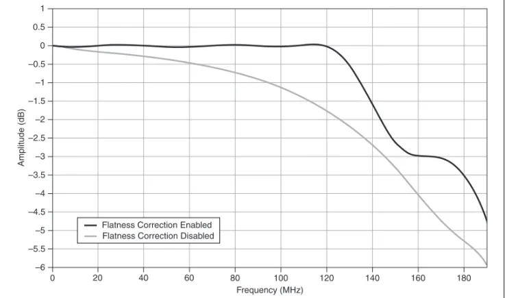
Frequency Response (Continued) Passband Flatness Flatness Correction Disabled Flatness Correction Enabled*,† With respect to 50 kHz into 100 differential load, 400 MS/s.† Flatness correction corrects for analog frequency response and DAC sinc response up to 0.3sample rate. Receiver return loss may degrade flatness. 0 MHz to 60 MHz†,‡ 0.5 dB, typical 0.24 dB 0.13 dB, typical 60 MHz†,‡ to 120 MHz†,** 1.9 dB, typical 0.34 dB 0.19 dB, typical Channel-to-Channel Passband Flatness Matching 0 MHz to 60 MHz†,‡
0.05 dB, typical 0.03 dB, typical With respect to 50 kHz on each channel, 400 MS/s. Load variations may degrade performance. Refer to the AC Amplitude Accuracy specification for more information about the 50 kHz reference accuracy. Channel-to-Channel Passband Flatness Matching 60 MHz†,‡ to 120 MHz†,** 0.18 dB, typical 0.04 dB, typical
* Valid for use without OSP enabled or when interpolating by 2x with OSP enabled. For all larger interpolation rates using
OSP, the OSP filters may introduce extra ripple. Refer to the Interpolating Flat Filter Passband Ripplespecification in the OSP section for more information about OSP filter ripple.
† Frequency ranges with flatness correction enabled are sample rate dependent. ‡ Value = Min (0.3 Sample Rate, 60 MHz)
** Value = 0.3 Sample Rate
Figure 1. Amplitude Response, Flatness Correction Enabled and Disabled,
400 MS/s, Differential, Referenced to 50 kHz, Typical
– 80 100– 120– 140– 160– 180– Frequency (MHz) – –6 – –5.5 – –5 – –4.5 – –3.5 – –4 – –3 – –2 – –2.5 – –1.5 – –1 – –0.5 – 0 – 1 – 0.5 0 – – 20 40– 60– 80– – 100 – 120 – 140 – 160 – 180 Amplitude (dB) Frequency (MHz) Flatness Correction Enabled
Flatness Correction Disabled
– –0.25 – –0.225 – –0.2 – –0.175 – –0.15 – –0.125 – –0.1 – –0.075 – –0.05 – –0.025 – 0 – 0.025 – 0.05 – 0.075 – 0.1 – 0.125 – 0.15 – 0.175 – 0.2 – 0.225 – 0.25 0– 20– 40– 60– 80– 100– 120– 140– 160– 180– Amplitude (dB) Frequency (MHz)
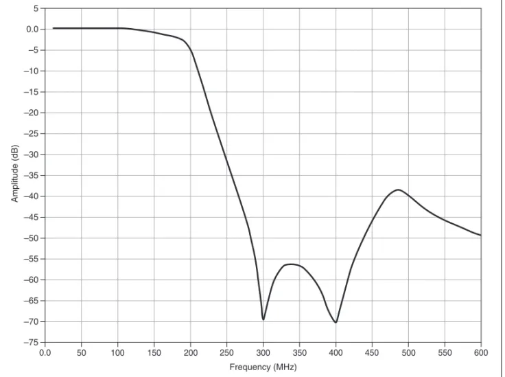
Figure 3. Characteristic Frequency Response of Image Suppression Filter, Typical Note Sinc response due to DAC sampling is not included in the previous figure.
– 0.0 50– – 100 – 150 – 200 – 250 300– – 350 – 400 450– 500– – 550 600– Frequency (MHz) Amplitude (dB) – –75 – –70 – –65 – –60 – –55 – –50 – –45 – –40 – –35 – –30 – –25 – –20 – –15 – –10 – –5 – 0.0 – 5
Specification Value Comments Spectral Characteristics Spurious-Free Dynamic Range (SFDR) at 1 MHz Frequency Range SFDR Without Harmonics (dB) SFDR With Harmonics (dB) Nominal. 400 MS/s, amplitude –1 dBFS. Includes aliased harmonics. Measured differentially. DC to 7 MHz 98 88 DC to 200 MHz 84 75 SFDR with Harmonics Frequency (MHz) SFDR (dB) 400 MS/s, amplitude –1 dBFS. Measured from DC to 200 MHz. Also called harmonic distortion. All values are typical and include aliased harmonics. Differential output measured single-ended with balun. 10 70 (74)* 60 68 (70)* 100 62 120 62 160 62 SFDR without Harmonics Frequency (MHz) SFDR (dB) 400 MS/s, amplitude –1 dBFS. Measured from DC to 200 MHz. All values are typical and include aliased harmonics. Differential output measured single-ended with balun. 10 70 (74)* 60 68 (73)* 100 64 120 62 160 62
* Long, nonrepetitive waveforms like modulated signals offer better spurious performance. For periodic waveforms
represented by a small number of unique samples, DAC nonlinearities limit dynamic specifications.
Spectral Characteristics (Continued)
Out of Band Performance
In-Band Tone Frequency (MHz)
Out of Band Spur Level (dBm) Nominal. Generating full-scale sine wave at frequency listed, 400 MS/s. Measured 200 MHz to 2 GHz. Anti-imaging filter is fixed and optimized for 400 MS/s. For more information, refer to Figure 3, Characteristic Frequency Response of Image Suppression Filter, Typical. Reduced sample rates degrade image rejection. 0 to 20 <–80 20 to 50 <–65 Channel-to- Channel Crosstalk <80 dBc, nominal, 0 MHz to 200 MHz <90 dBc, nominal, 0 MHz to 150 MHz —
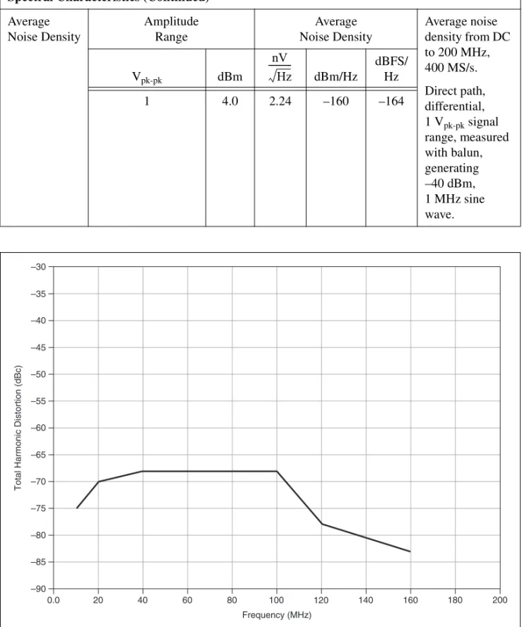
Spectral Characteristics (Continued) Total Harmonic Distortion (THD) Frequency (MHz) THD (dBc) Amplitude –1 dBFS. Includes the 2nd through the 6th harmonic. All values are typical. Differential output measured single-ended with balun. Measured at 0.1 MHz offset. 400 MS/s sample rate. 10 –75 20 –70 40 –68 80 –68 100 –68 120 –78 160 –83 Intermodula- tion Distortion (IMD3)
Frequency (MHz) IMD (dBc) Amplitude
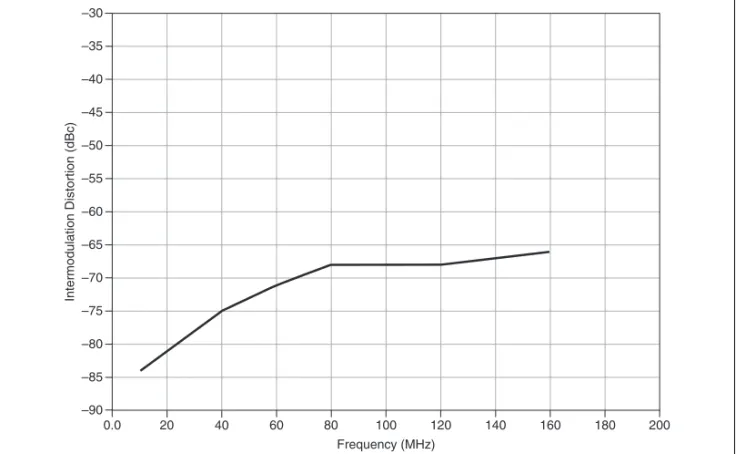
–7 dBFS. All values are typical. Differential output measured single-ended with balun. 400 MS/s sample rate. Two-tone frequencies are frequency ±100 kHz. 10 –84 20 –81 40 –75 60 –71 80 –68 120 –68 160 –66
Figure 4. Total Harmonic Distortion, Typical
Spectral Characteristics (Continued)
Average Noise Density Amplitude Range Average Noise Density Average noise density from DC to 200 MHz, 400 MS/s. Direct path, differential, 1 Vpk-pk signal range, measured with balun, generating –40 dBm, 1 MHz sine wave. Vpk-pk dBm dBm/Hz dBFS/ Hz 1 4.0 2.24 –160 –164
Specification Value Comments
nV Hz ---– 0.0 – 20 – 40 – 60 – 80 – 100 Frequency (MHz)
Total Harmonic Distortion (dBc)
– 120 – 140 – 160 – 180 – 200 – – – – – – – – – – – – – –90 –85 –80 –75 –70 –65 –60 –55 –50 –45 –40 –35 –30
Figure 5. Intermodulation Distortion, 200 kHz Separation, Typical – 0.0 20– 40– 60– 80– 100– 120– 140– 160– 180– 200– Frequency (MHz) Intermodulation Distortion (dBc) – –90 – –85 – –80 – –75 – –70 – –65 – –60 – –55 – –50 – –45 – –40 – –35 – –30 – 5 20– 40– 60– 80– 100– 120– 140– 160– 180– – 200 Frequency (MHz) Amplitude (dBm) – –95 – –90 – –80 – –70 – –60 – –50 – –40 – –30 – –20 – –10 – 0.0 – –– –– –– –– –– –– –– –– –– – – –
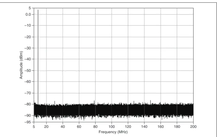
Figure 7. 10.000 MHz Single-Tone Spectrum, 400 MS/s, –1 dBFS, Typical
Figure 8. 10.100 MHz Single-Tone Spectrum, 400 MS/s, –1 dBFS, Typical
– 5 20– 40– 60– 80– 100– 120– 140– 60– 180– 200– Frequency (MHz) Amplitude (dBm) – –95 – –90 – –80 – –70 – –60 – –50 – –40 – –30 – –20 – –10 – 0.0 – 5 – – – – – – – 5 20– 40– 60– 80– 100– 120– 140– 160– – 180 200– Frequency (MHz) Amplitude (dBm) – –95 – –90 – –80 – –70 – –60 – –50 – –40 – –30 – –20 – –10 – 0.0 – 5
Specification Value Comments Output Phase Noise and Jitter*
Sample Clock Source Output Freq. (MHz)
System Phase Noise Density† (dBc/Hz) System
Output Integrated Jitter† 100 Hz 1 kHz 10 kHz 100 kHz 1 MHz Internal, High Resolution Clock, 400 MS/s 10 <–121 <–137 <–146 <–152 <–153 <350 fs Typical. 100 <–101 <–119 <–126 <–136 <–141 <350 fs CLK IN External 10 MHz Reference Clock 400 MS/s 10 <–122 <–135 <–146 <–152 <–153 <350 fs Typical. 100 <–105 <–115 <–126 <–136 <–141 <350 fs
* Using an external Sample clock at some frequencies may introduce phase noise spurs due to external clock beating with onboard
clock.
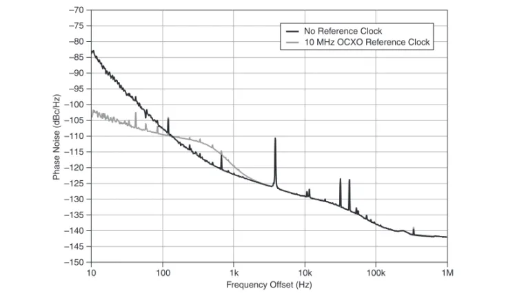
Figure 9. Phase Noise on a Representative Module, 100 MHz Sine Wave,
400 MS/s Internal Clock Sample Rate, Chassis Fans Low, Shown With and Without a Reference Clock
Figure 10. Phase Noise on a Representative Module, 100 MHz Sine Wave,
400 MS/s Internal Clock Sample Rate, Chassis Fans High, No Reference Clock –70 –150 –145 –140 –135 –130 –125 –120 –115 –110 –105 –100 –95 –90 –85 –80 –75 1M 10 100 1k 10k 100k Phase Noise (dBc/Hz) Frequency Offset (Hz) No Reference Clock
10 MHz OCXO Reference Clock
Phase Noise (dBc/Hz) –70 –150 –145 –140 –135 –130 –125 –120 –115 –110 –105 –100 –95 –90 –85 –80 –75 Frequency Offset (Hz) 1M 10 100 1k 10k 100k No Reference Clock
Specification Value Comments Suggested Maximum Frequencies for Common Functions
Sine 145 MHz The NI 5450
is optimized for frequency-domain performance. Square 33 MHz (<133 V/s slew rate)*
Ramp 1 MHz (<50 V/s slew rate)*
Triangle 8 MHz
Pulse Response
Flatness Correction Disabled Flatness Correction Enabled Typical. Values into 50 Rise/Fall Time (10% to 90%) 3 ns 2.5 ns Aberration 18% (7%)† 22%
* Aberrations on pulsed waveforms are due to the analog reconstruction filter and can be significantly reduced if waveform
data has limited slew rate. Waveforms with higher slew rates are not recommended.
† 7% aberrations achievable with 133 V/s slew rate limiting on waveform data. Pulsed waveforms should contain multiple
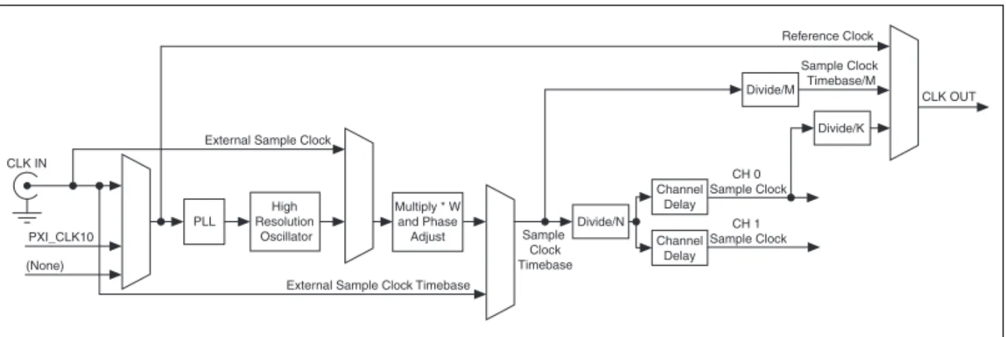
Clocking
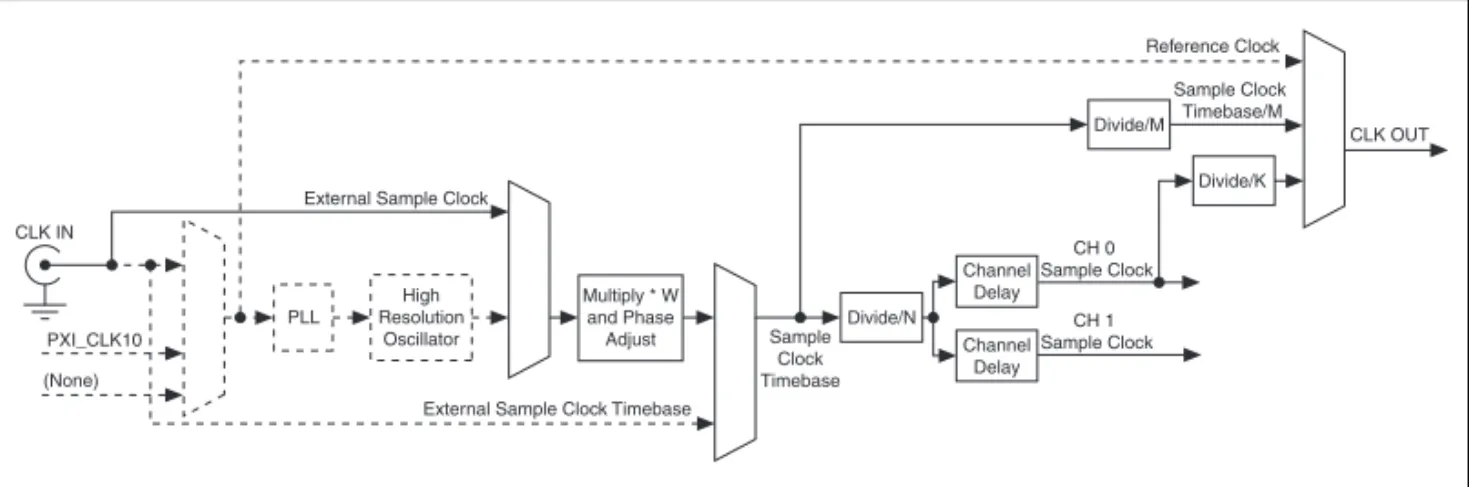
The clocking of the NI 5450 is very flexible. Waveform generation is driven by the Sample clock. You have multiple choices for configuring the device clocking, as shown in the following figure.
Figure 11. NI PXIe-5450 Clocking
Tip Refer to the clocking documentation in the NI Signal Generators Help by navigating to NI Signal Generators Help»Devices»NI 5450»Theory of Operation»Clocking for more information about clocking options on the NI 5450.
PXI_CLK10 CLK IN High Resolution Oscillator PLL CLK OUT (None) Divide/M Sample Clock Timebase/M Multiply * W and Phase Adjust Divide/N Sample Clock Timebase Channel Delay Channel Delay CH 0 Sample Clock CH 1 Sample Clock Divide/K Reference Clock
External Sample Clock
Onboard Sample Clock
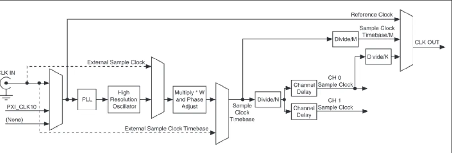
The following figure shows the NI 5450 onboard Sample clock path.
Figure 12. NI PXIe-5450 Onboard Sample Clock and External Reference Clock Path
Specification Value Comments
Sample Clock Rate Range 12.2 kS/s to 400 MS/s — Sample Clock Rate Frequency Resolution <5.7 Hz Varies with Sample clock frequency. Specification is worst-case. Sample Clock Delay
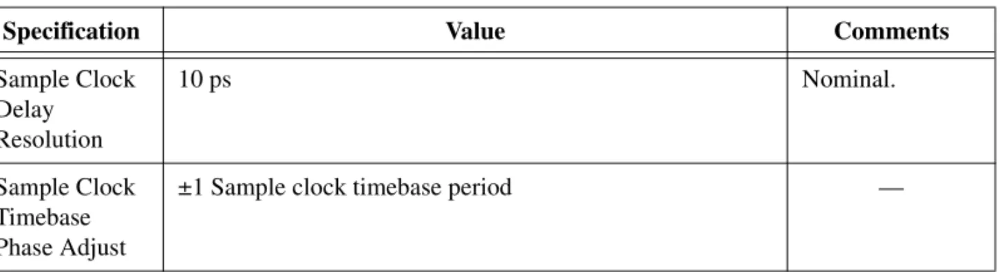
0 ns to 2 ns, independent per channel Set in software with the Channel Delay property or the NIFGEN_ATTR_ CHANNEL_DELAY attribute. Sample Clock Delay Resolution 10 ps Nominal. Sample Clock Timebase Phase Adjust
±1 Sample clock timebase period —
Reference Clock Sources
1. None (internal reference) 2. PXI_CLK10 (backplane) — PXI_CLK10 CLK IN High Resolution Oscillator PLL CLK OUT (None) Divide/M Sample Clock Timebase/M Multiply * W and Phase Adjust Divide/N Sample Clock Timebase Channel Delay Channel Delay CH 0 Sample Clock CH 1 Sample Clock Divide/K Reference Clock
External Sample Clock
Reference Clock Frequency 1 MHz to 100 MHz in increments of 1 MHz 100 MHz to 200 MHz in increments of 2 MHz 200 MHz to 400 MHz in increments of 4 MHz Default of 10 MHz. ±0.01% accuracy required. Internal Reference Clock Frequency Accuracy ±0.01% Measured without an external Reference clock. When locking to a Reference clock, frequency accuracy is solely dependent on the frequency accuracy of the Reference clock source.
External Sample Clock
The following figure shows the NI 5450 external Sample clock path.
Figure 13. NI PXIe-5450 External Sample Clock Path
Specification Value Comments
External Sample Clock Source
CLK IN, front panel connector, with multiplication and division — External Sample Clock Rate 10 MS/s, 20 MS/s to 400 MS/s — Sample Clock Rate Range 12.2 kS/s to 400 MS/s — Multiplication/ Division Factor Range
Varies depending on the external Sample clock rate Shown as Multiply*W and Divide/N in Figure 13, NI PXIe-5450 External Sample Clock Path. Sample Clock Delay
0 ns to 2 ns, independent per channel Set in software with the Channel Delay property or the NIFGEN_ATTR_ CHANNEL_DELAY attribute. PXI_CLK10 CLK IN High Resolution Oscillator PLL CLK OUT (None) Divide/M Sample Clock Timebase/M Multiply * W and Phase Adjust Divide/N Sample Clock Timebase Channel Delay Channel Delay CH 0 Sample Clock CH 1 Sample Clock Divide/K Reference Clock
External Sample Clock
External Sample Clock Timebase
The following figure shows the NI 5450 external Sample clock timebase path.
Figure 14. NI PXIe-5450 External Sample Clock Timebase Path
Sample Clock Delay Resolution 10 ps Nominal. Sample Clock Timebase Phase Adjust
±1 Sample clock timebase period —
Specification Value Comments
External Sample Clock Timebase Sources
CLK IN, front panel connector, with division —
External Sample Clock Timebase Rate Range 200 MS/s to 400 MS/s — Divide Factor Range 1, 2 to 32,768 in steps of 2 Shown as Divide/N in Figure 14, NI PXIe-5450 External Sample Clock Timebase Path.
Specification Value Comments
PXI_CLK10 CLK IN High Resolution Oscillator PLL CLK OUT (None) Divide/M Sample Clock Timebase/M Multiply * W and Phase Adjust Divide/N Sample Clock Timebase Channel Delay Channel Delay CH 0 Sample Clock CH 1 Sample Clock Divide/K Reference Clock
External Sample Clock
Exporting Clocks
Sample Clock Delay0 ns to 2 ns, independent per channel —
Sample Clock Delay Resolution
10 ps Nominal.
Specification Value Comments
Destination Rates
Reference Clock
CLK OUT 1 MHz to 400 MHz —
PFI<0..1> 1 MHz to 200 MHz
Sample Clock CLK OUT 100 kHz to 400 MHz With optional
divider. PFI<0..1> 0 MHz to 200 MHz
Sample Clock Timebase
CLK OUT 100 kHz to 400 MHz With optional
divider. PFI<0..1> 0 MHz to 200 MHz
Terminals
CLK IN
(Sample Clock and Reference Clock Input, Front Panel Connector)
Specification Value Comments
Direction Input —
Destinations 1. Reference clock 2. Sample clock
3. Sample clock timebase
— Frequency Range 1 MHz to 400 MHz Not applicable for all destinations. Refer to the specifications for your clocking configuration for applicable ranges. Input Voltage Range 500 mVpk-pk to 5 Vpk-pk into 50 (–2 dBm to +18 dBm) 50% duty cycle input. 550 mVpk-pk to 4.5 Vpk-pk into 50 (–1.2 dBm to +17 dBm) 45% to 55% duty cycle input. Input Protection Range 6 Vpk-pk into 50 19.5 dBm 50% duty cycle input. 5.4 Vpk-pk into 50 18.5 dBm 45% to 55% duty cycle input. Duty Cycle Requirements 45% to 55% — Input Impedance 50 , nominal — Input Coupling AC — Voltage Standing Wave Ratio (VSWR) 1.3:1 up to 2 GHz Nominal.
CLK OUT
(Sample Clock and Reference Clock Output, Front Panel Connector)
PFI 0 and PFI 1
(Programmable Function Interface, Front Panel Connectors)
Specification Value Comments
Direction Output —
Sources 1. Sample clock, divided by integer K (1 K 3, minimum) 2. Reference clock
3. Sample clock timebase, divided by integer M (1 M 1048576) The maximum value of the divisor, K, is sample rate dependent. Frequency Range 100 kHz to 400 MHz —
Output Voltage 0.7 Vpk-pk into 50 Typical.
Maximum Output Overload 3.3 Vpk-pk from a 50 source — Output Coupling AC — VSWR 1.3:1 up to 2 GHz Nominal.
Specification Value Comments
Direction Bidirectional —
Frequency Range
DC to 200 MHz —
As an Input (Trigger)
Destinations Start trigger, Script trigger —
Input Range 0 V to 5 V —
Input Protection Range
As an Input (Trigger) (Continued) VIH 1.8 V — VIL 1.5 V — Input Impedance 10 k, nominal — As an Output (Event)
Sources 1. Sample clock divided by integer K (2 K 3, minimum) 2. Sample clock timebase divided by integer M
(2 M 1,048,576) 3. Reference clock 4. Marker event 5. Data marker event 6. Exported Start trigger 7. Exported Script trigger 8. Ready for Start event 9. Started event 10. Done event The maximum value of the Sample clock divisor, K, is sample rate dependent. Output Impedance 50 , nominal — Maximum Output Overload –2 V to +6.5 V —
VOH Minimum: 2.4 V (open load), 1.3 V (50 load) Output drivers
are +3.3 V TTL/CMOS compatible up to 200 MHz. VOL Maximum: 0.4 V (open load), 0.2 V (50 load)
Rise/Fall Time 3 ns Typical. Load of
10 pF.
Triggers and Events
Triggers
Specification Value Comments
Sources 1. PFI<0..1> (SMB front panel connectors) 2. PXI_Trig<0..7> (backplane connector)
3. Immediate (does not wait for a trigger). Default.
—
Types 1. Start trigger edge
2. Script trigger edge and level 3. Software trigger
—
Edge Detection Rising, falling —
Minimum Pulse Width 25 ns Refer to the ts1 documentation in the NI Signal Generators Help by navigating to NI Signal Generators Help»Devices» NI 5450» Triggering» Trigger Timing. Delay from Trigger to Analog Output with OSP Disabled
154 Sample clock timebase periods + 65 ns, nominal Refer to the ts2 documentation in the NI Signal Generators Help by navigating to NI Signal Generators Help»Devices» NI 5450» Triggering» Trigger Timing. Additional Delay with OSP Enabled
Trigger Exporting
Exported Trigger Destinations
1. PFI<0..1> (SMB front panel connectors) 2. PXI_Trig<0..6> (backplane connector)
—
Exported Trigger Delay
50 ns, nominal Refer to the ts3
documentation in the NI Signal Generators Help by navigating to NI Signal Generators Help»Devices» NI 5450» Triggering» Trigger Timing. Exported Trigger Pulse Width >150 ns Refer to the ts4 documentation in the NI Signal Generators Help by navigating to NI Signal Generators Help»Devices» NI 5450» Triggering» Trigger Timing.
Events
Specification Value Comments
Destinations 1. PFI<0..1> (SMB front panel connectors) 2. PXI_Trig<0..6> (backplane connector)
—
Types Marker<0..3>, Data Marker<0..1>, Ready for Start, Started, Done
There are two data markers per channel. Quantum Marker position must be placed at an integer multiple of
two samples.
—
Width Adjustable, minimum of 2 samples. Default is 150 ns. Refer to the tm2 documentation in the NI Signal Generators Help by navigating to NI Signal Generators Help» Fundamentals» Waveform Fundamentals» Events» Marker Events. Skew Destination With Respect to Analog Output Refer to the tm1 documentation in the NI Signal Generators Help by navigating to NI Signal Generators Help» Fundamentals» Waveform Fundamentals» Events» Marker Events.
PFI<0..1> ±3 Sample clock periods PXI_Trig<0..6> ±6 Sample clock periods
Waveform Generation Capabilities
Specification Value Comments
Memory Usage
The NI 5450 uses the Synchronization and Memory Core (SMC) technology in which waveforms and instructions share onboard memory. Parameters, such as number of segments in sequence list, maximum number of
waveforms in memory, and number of samples available for waveform storage, are flexible and user defined.
For more information, refer to the NI Signal Generators Help by navigating to NI Signal Generators Help» Programming» Reference» NI-TClk Synchronization Help. Onboard Memory Size 128 MB option: 134,217,728 bytes 512 MB option: 536,870,912 bytes Memory is shared between both channels. Loop Count 1 to 16,777,215
Burst trigger: Unlimited
—
Quantum Waveform size must be an integer multiple of two samples — Output Modes Arbitrary Waveform mode
A single waveform is selected from the set of waveforms stored in onboard memory and generated.
—
Script mode A script allows you to link and loop multiple waveforms in complex combinations. A script is a series of
instructions that indicates how waveforms saved in the onboard memory should be sent to the device. The script can specify the order in which the waveforms are generated, the number of times they are generated, and the triggers and markers associated with the generation.
Output Modes (Continued)
Arbitrary Sequence mode
A sequence directs the NI 5450 to generate a set of waveforms in a specific order. Elements of the sequence are referred to as segments. Each segment is associated with a set of instructions. The instructions identify which waveform is selected from the set of waveforms in memory, how many loops (iterations) of the waveform are generated, and at which sample in the waveform a marker output signal is sent.
—
Minimum Waveform Size (Samples)
Trigger Mode Number of Channels Arbitrary Waveform Mode Arbitrary Sequence Mode >180 MS/s Arbitrary Sequence Mode 180 MS/s The minimum waveform size is sample rate dependent. Measured using a 200 MHz trigger. Single 1 4 2 2 2 4 4 4 Continuous 1 142 140 58 2 284 280 116 Stepped 1 210 154 54 2 420 308 108 Burst 1 142 1,134 476 2 284 2,312 952
Memory Limits (bytes) Number of Channels 128 MB 512 MB Arbitrary Waveform Mode, Maximum Waveform Memory
1 67,108,352 268,434,944 All trigger modes
except where noted.
2 33,553,920 134,217,216 Arbitrary Sequence Mode, Maximum Waveform Memory 1 67,108,352 268,434,944 Condition: One or two segments in a sequence. 2 33,553,920 134,217,216 Arbitrary Sequence Mode, Maximum Waveforms 1 1,048,575 4,194,303 Condition: One or two segments in a sequence. 2 524,287 2,097,151 Arbitrary Sequence Mode, Maximum Segments in a Sequence 1 8,388,597 33,554,421 Condition: Waveform size is <4,000 samples. 2 4,194,293 16,777,205
Waveform Play Times Maximum Play Time, Sample Rate Number of Channels 128 MB 512 MB Single Trigger mode.
Play times can be significantly extended by using Continuous, Stepped, or Burst Trigger modes. 400 MS/s 1 0.17 seconds 0.67 seconds 2 0.084 seconds 0.34 seconds 25 MS/s 1 2.68 seconds 10.74 seconds 2 1.34 seconds 5.37 seconds 100 kS/s 1 11 minutes 11 seconds 44 minutes 44 seconds 2 5 minutes 35 seconds 22 minutes 22 seconds
Onboard Signal Processing
Figure 15. Onboard Signal Processing Block Diagram
Specification Value Comments
I/Q Rate OSP Interpolation Range 2, 4, 8, 12, 16, 20 24 to 8,192 (multiples of 8) 8,192 to 16,384 (multiples of 16) 16,384 to 32,768 (multiples of 32) —
I/Q Rate (Sample clock rate) ÷ (OSP interpolation) Example: For a
Sample clock rate of 400 MS/s, I/Q rate range = 12.2 kS/s to 200 MS/s.
Bandwidth 0.4I/Q rate, per output When using an
external I/Q modulator, RF bandwidth = 0.8I/Q Rate. Data Processing Modes
1. Real (I path only) 2. Complex (I/Q)
—
OSP Mode Baseband —
Pre-Filter Gain I Pre-Filter Offset I Filtering and Interpolation I Onboard Signal Processing
Digital Gain I DAC I Output Engine Waveform Memory Pre-Filter Gain Q Pre-Filter Offset Q Filtering and Interpolation Q Digital Gain Q DAC Q Programmable I/Q Gain & Offset Control
Pulse Shaping and Interpolation Frequency Shift I/Q Rate
Prefilter Gain and Offset Prefilter Gain and Offset Resolution 21 bits — Prefilter Gain Range –16.0 to +16.0
(|Values| < 1 attenuate user data)
Unitless. Prefilter Offset Range –1.0 to +1.0 Applied after prefilter gain. Prefilter Output
(User data Prefilter gain) + Prefilter offset Overflows occur when |Output| > 1.
Finite Impulse Response (FIR) Filtering
Filter Types Parameter Minimum Maximum
Flat Passband 0.4 0.4 Lowpass filter
that minimizes ripple to: I/Q rate passband.
Raised Cosine Alpha 0.1 0.4 When using pulse
shaping, these filters require an OSP interpolation factor of 24 or greater. Root Raised Cosine Alpha 0.1 0.4
Numerically Controlled Oscillator (NCO)
Maximum Frequency
0.4 sample rate Frequency shift
using the NCO is a quadrature (complex) operation. Frequency
Resolution
Sample rate/248 Example:
1.42Hz with a sample rate of 400 MS/s.
Tuning Speed 250 s Typical.
Software- and system-
Calibration
Digital Performance Maximum NCO Spur <–90 dBc Full-scale output. Interpolating Flat Filter Passband Ripple <0.1 dB Passband from 0 to (0.4I/Q Rate). Ripple is dependent upon the interpolation rate. Interpolating Flat Filter Out-of-Band Suppression >80 dB Stopband suppression from (0.6 I/Q rate).Specification Value Comments
External Calibration
The external calibration calibrates the ADC voltage reference and passband flatness. Appropriate constants are stored in nonvolatile memory.
—
Self-Calibration An onboard, 24-bit ADC and precision voltage reference are used to calibrate the DC gain and offset. Onboard channel alignment circuitry is used to calibrate the skew between channels. The self-calibration is initiated by the user through the software and takes approximately 60 seconds to complete. Appropriate constants are stored in nonvolatile memory.
—
Calibration Interval
Specifications valid within 1 year of external calibration —
Warm-up Time 15 minutes —
Power
Software
Specification Typical Maximum Comments
+3.3 VDC 1.9 A 2.0 A —
+12 VDC 2.2 A 2.5 A —
Total Power 32.7 W 36.6 W —
Specification Value Comments
Driver Software
NI-FGEN is an IVI-compliant driver that allows you to configure, control, and calibrate the NI 5450. NI-FGEN provides application programming interfaces for many development environments.
—
Application Software
NI-FGEN provides programming interfaces for the following application development environments: • LabVIEW
• LabWindows™/CVI™
• Measurement Studio • Microsoft Visual C++ .NET • Microsoft Visual C/C++ • Microsoft Visual Basic
—
Interactive Control and Configuration Software
The FGEN Soft Front Panel supports interactive control of the NI 5450. The FGEN Soft Front Panel is included on the NI-FGEN driver CDs.
Measurement & Automation Explorer (MAX) provides interactive configuration and test tools for the NI 5450. MAX is also included on the NI-FGEN CDs.
You can use the NI 5450 with NI SignalExpress.
Physical
Hardware Front Panel
Figure 16. NI 5450 Front Panel 5 Vp-p MAX, 50 Ω 50 Ω 0.7 Vp-p NOM 50 Ω LVT T L 50 Ω 50 Ω ESD SENSITIVE LVT T L
Specification Value Comments
Dimensions 3U, Two Slot, PXI Express module 21.6 cm × 4.0 cm × 13.0 cm (8.5 in. × 1.6 in. × 5.1 in.)
—
Weight 476 g (17 oz) —
Front Panel Connectors
Label Function(s) Connector Type
CH 0+/I+ Differential Analog Output SMA —
CH 0–/I– Differential Analog Output SMA
CH 1+/Q+ Differential Analog Output SMA
CH 1–/Q– Differential Analog Output SMA
CLK IN Sample clock, Sample clock timebase, and Reference clock input.
SMA
CLK OUT Sample clock, Sample clock timebase, and Reference clock output.
SMA
PFI 0 Marker output, trigger input, Sample clock output, exported trigger output.
SMB
PFI 1 Marker output, trigger input, Sample clock output, exported trigger output.
SMB
Front Panel LED Indicators
Label Function
ACCESS The ACCESS LED indicates the status of the PXI Express bus and the interface from the NI 5450 to the controller.
For more information about the front panel LEDs, refer to the NI Signal Generators Help. ACTIVE The ACTIVE LED indicates the status of the onboard
NI PXIe-5450 Environment
Note To ensure that the NI PXIe-5450 cools effectively, follow the guidelines in the Maintain Forced-Air Cooling Note to Users included in the NI 5450 kit. The NI PXIe-5450 is intended for indoor use only.
Specifications Value Comments
Operating Temperature
0 ºC to +55 ºC in all NI PXI Express chassis: Meets IEC 60068-2-1 and IEC 60068-2-2.
Note: Refer to KnowledgeBase 4AEB2ML1 at ni.com
for more information about maximizing PXI Express data transfer rates when operating at ambient temperatures below 10 ºC.
—
Storage Temperature
–25 ºC to +85 ºC. Meets IEC 60068-2-1 and IEC 60068-2-2. —
Operating Relative Humidity
10% to 90%, noncondensing. Meets IEC 60068-2-56. —
Storage Relative Humidity
5% to 95%, noncondensing. Meets IEC 60068-2-56. —
Operating Shock
30 g, half-sine, 11 ms pulse. Meets IEC 60068-2-27. Test profile developed in accordance with MIL-PRF-28800F.
Spectral and jitter specifications could degrade. Storage Shock 50 g, half-sine, 11 ms pulse. Meets IEC 60068-2-27. Test
profile developed in accordance with MIL-PRF-28800F.
—
Operating Vibration
5 Hz to 500 Hz, 0.31 grms. Meets IEC 60068-2-64. Spectral and jitter
specifications could degrade. Storage
Vibration
5 Hz to 500 Hz, 2.46 grms. Meets IEC 60068-2-64. Test
profile exceeds requirements of MIL-PRF-28800F, Class B.
—
Altitude 2,000 meter maximum (at 25 °C ambient temperature) —
Pollution Degree
Safety
This product meets the requirements of the following standards of safety for electrical equipment for measurement, control, and laboratory use: • IEC 61010-1, EN 61010-1
• UL 61010-1, CSA 61010-1
Note For UL and other safety certifications, refer to the product label or the Online Product Certification section.
Electromagnetic Compatibility
This product meets the requirements of the following EMC standards for electrical equipment for measurement, control, and laboratory use: • EN 61326 (IEC 61326): Class A emissions; Basic immunity • EN 55011 (CISPR 11): Group 1, Class A emissions
• AS/NZS CISPR 11: Group 1, Class A emissions • FCC 47 CFR Part 15B: Class A emissions • ICES-001: Class A emissions
Note For the standards applied to assess the EMC of this product, refer to the Online Product Certification section.
Note For EMC compliance, operate this product according to the documentation.
CE Compliance
This product meets the essential requirements of applicable European Directives as follows:
• 2006/95/EC; Low-Voltage Directive (safety)
• 2004/108/EC; Electromagnetic Compatibility Directive (EMC)
Online Product Certification
Refer to the product Declaration of Conformity (DoC) for additional regulatory compliance information. To obtain product certifications and the DoC for this product, visit ni.com/certification, search by model number or product line, and click the appropriate link in the Certification column.
Environmental Management
National Instruments is committed to designing and manufacturing products in an environmentally responsible manner. NI recognizes that eliminating certain hazardous substances from our products is beneficial not only to the environment but also to NI customers.
For additional environmental information, refer to the NI and the
Environment Web page at ni.com/environment. This page contains the environmental regulations and directives with which NI complies, as well as other environmental information not included in this document.
Waste Electrical and Electronic Equipment (WEEE)
EU Customers At the end of the product life cycle, all products must be sent to a WEEE
recycling center. For more information about WEEE recycling centers, National Instruments WEEE initiatives, and compliance with WEEE Directive 2002/96/EC on Waste and Electronic Equipment, visit ni.com/environment/weee.
⬉ᄤֵᙃѻક∵ᶧࠊㅵ⧚ࡲ⊩ ˄Ё
RoHS
˅
Ёᅶ᠋ National Instrumentsヺড়Ё⬉ᄤֵᙃѻકЁ䰤ࠊՓ⫼ᶤѯ᳝ᆇ⠽䋼ᣛҸ (RoHS)DŽ ݇ѢNational InstrumentsЁRoHSড়㾘ᗻֵᙃˈ䇋ⱏᔩ ni.com/environment/rohs_chinaDŽ (For information about China RoHS compliance, go to ni.com/environment/rohs_china.)
CVI, LabVIEW, National Instruments, NI, ni.com, the National Instruments corporate logo, and the Eagle logo are trademarks of National Instruments Corporation. Refer to the Trademark Information at ni.com/trademarks for other National Instruments trademarks. The mark LabWindows is used under a license from Microsoft Corporation. Windows is a registered trademark of Microsoft
Where to Go for Support
The National Instruments Web site is your complete resource for technical support. At ni.com/support you have access to everything from troubleshooting and application development self-help resources to email and phone assistance from NI Application Engineers.
A Declaration of Conformity (DoC) is our claim of compliance with the Council of the European Communities using the manufacturer’s declaration of conformity. This system affords the user protection for electromagnetic compatibility (EMC) and product safety. You can obtain the DoC for your product by visiting ni.com/certification. If your product supports calibration, you can obtain the calibration certificate for your product at ni.com/calibration.
National Instruments corporate headquarters is located at 11500 North Mopac Expressway, Austin, Texas, 78759-3504. National Instruments also has offices located around the world to help address your support needs. For telephone support in the United States, create your service request at ni.com/support and follow the calling instructions or dial 512 795 8248. For telephone support outside the United States, contact your local branch office:
Australia 1800 300 800, Austria 43 662 457990-0, Belgium 32 (0) 2 757 0020, Brazil 55 11 3262 3599, Canada 800 433 3488, China 86 21 5050 9800,
Czech Republic 420 224 235 774, Denmark 45 45 76 26 00, Finland 358 (0) 9 725 72511, France 01 57 66 24 24,
Germany 49 89 7413130, India 91 80 41190000, Israel 972 3 6393737, Italy 39 02 41309277, Japan 0120-527196, Korea 82 02 3451 3400, Lebanon 961 (0) 1 33 28 28, Malaysia 1800 887710,
Mexico 01 800 010 0793, Netherlands 31 (0) 348 433 466, New Zealand 0800 553 322, Norway 47 (0) 66 90 76 60, Poland 48 22 328 90 10, Portugal 351 210 311 210, Russia 7 495 783 6851, Singapore 1800 226 5886, Slovenia 386 3 425 42 00, South Africa 27 0 11 805 8197, Spain 34 91 640 0085, Sweden 46 (0) 8 587 895 00, Switzerland 41 56 2005151, Taiwan 886 02 2377 2222, Thailand 662 278 6777, Turkey 90 212 279 3031, United Kingdom 44 (0) 1635 523545
NI PXIe-5450
仕様
400 MS/s
差動
I/Q
信号発生器
このドキュメントには、NI PXIe-5450(NI 5450)差動I/Q信号発生器の 仕様が記載されています。 仕様は、以下の条件下において保証されています。 • 周囲温度での15分間のウォームアップ時間 • 一定に維持されたキャリブレーション間隔 • シャーシのファンの速度をHIGHに設定 • NI-FGEN計測器ドライバを使用 • 計測器が安定した後にNI-FGEN計測器ドライバセルフキャリブレー ションを実行 特に注記のない限り、各仕様において以下の条件が適用されます。 • 50 Ωで信号をグランドに終端。 • ダイレクトパスを0.5 Vpk差動(ゲイン = 0.5、1 Vpk-pk差動)に設定 • サンプルクロックは400 MS/sに設定 • 基準クロックなしのオンボードサンプルクロック • 0~55℃の周囲温度 仕様は、特に指定がない限り、0~55℃の周囲温度範囲内で使用した場 合の、保証済みでトレーサブルな製品性能を記載しています。 標準値は、保証範囲外での使用における有用な製品性能を表しますが、こ れには測定の不確定性やドリフトに対するガードバンドは含まれていませ ん。標準値は工場から出荷されたすべてのユニットで確認されるとは限り ません。特に指定がない限り、標準値は、この製品の開発時または製造時 の測定値に基づいて、23 ±5℃(信頼水準90%)の周囲温度範囲内で使 用した場合の、ユニットの予想性能を記載しています。 公称値(または補足情報)は、仕様または標準値に記載されていない予想 性能を含む、製品の有用な追加情報を記載しています。公称値は保証範囲 外です。 仕様は事前の通知なしに変更されることがあります。最新のNI 5450の仕 様については、ni.com/manualsをご覧ください。 NI 5450のドキュメントにアクセスするには、スタート→すべてのプログ ラム→National Instruments→NI-FGEN→ドキュメントを選択します。熱面 NI 5450を長時間使用する場合、デバイスまたはシールドは安全な取扱温度を超 え、火傷の原因になる場合があります。シールドに触れる前、またはデバイスを シャーシから取り外す前に、NI 5450を十分に冷却してください。 注意 機能的な理由により、この高感度テストおよび測定製品の出力は電磁妨害に対 して保護されていません。その結果、電磁妨害がある環境でケーブルが接続され ている場合、この製品では確度が低下したり、その他の性能が一時的に劣化す ることがあります。
目次
アナログ出力...3 CH 0+/–、CH 1+/– (アナログ出力、フロントパネルコネクタ)...3 クロック... 18 オンボードサンプルクロック... 19 外部サンプルクロック... 20 外部サンプルクロックタイムベース... 22 クロックをエクスポートする... 23 端子... 23 CLK IN (サンプルクロックおよび基準クロック入力、 フロントパネルコネクタ)... 23 CLK OUT (サンプルクロックおよび基準クロック出力、 フロントパネルコネクタ)... 25 PFI 0およびPFI 1 (プログラム可能な機能的インタフェース、 フロントパネルコネクタ)... 25 トリガおよびイベント... 27 トリガ... 27 イベント... 28 波形生成機能... 29 オンボード信号処理... 32 キャリブレーション... 34 電源... 35 ソフトウェア... 35 物理特性... 36 ハードウェアのフロントパネル... 36 NI PXIe-5450の環境... 38 安全性... 39 電磁両立性... 39 CEマーク準拠... 39 オンライン製品認証... 39 ... 40アナログ出力
CH 0+/
–
、
CH 1+/
–
(アナログ出力、フロントパネルコネクタ)
仕様 値 コメント チャンネル数 2 — 出力タイプ 差動 — 出力パス ダイレクトパス — DAC分解能 16ビット — 振幅とオフセット 差動フルス ケール振幅範 囲 フラットネ ス補正状態 負荷 振幅 (Vpk-pk)* CH 0+/–または CH 1+/–端子は 両方とも同じ値 の負荷でグラン ドに終端。 差動Vpk-pkとし て測定。各端子の Vpk-pkは、差動 Vpk-pkの半分の 値。 最小値 最大値 無効 50 Ω 0.708 1.00 1 kΩ 1.35 1.90 開回路 1.42 2.00 有効 50 Ω 0.567 0.8 1 kΩ 1.08 1.52 開回路 1.14 1.6 振幅分解能 4桁 < 0.0025%(振幅範囲の0.0002 dB) — * 振幅値は、DACのフルスケールが利用されていると仮定。最小値よりも小さい振幅を必要とする場合は、DACのフルス ケールよりも小さい波形またはデジタルゲインが使用可能。 NI-FGENのゲイン値は、Vpk-pkの半分の振幅であるVpkに相当。確度 DC確度 絶対値 ゲインエラー: セルフキャリブレーション温度±5℃以内の場合: 差動出力範囲の±0.2%* セルフキャリブレーション温度±5℃を上回る場合: + 0.030%/℃ + 0.015%/℃、標準 差動オフセット: ± 1 mV(0~55℃) コモンモードオフセット†: ±350 μV(0~55℃) チャンネル間、相対 ゲインエラー: セルフキャリブレーション温度±5℃以内の場合: 差動出力範囲の±0.08%* セルフキャリブレーション温度±5℃を上回る場合: + 0.010%/℃ + 0.005%/℃、標準 DMMで測定。 セルフキャリブ レーション中、 差動オフセット は未調整。 高インピーダン スでグランドに 終端された両方 の出力端子で測 定。 * DC確度の場合、差動出力範囲は、高インピーダンスのゲイン設定の2倍に定義。たとえば、ゲイン値が1、負荷インピー ダンスが1 GΩ、差動出力範囲が2 VのDC信号確度は、以下の式によって計算。 セルフキャリブレーション温度±5℃以内のゲイン誤差: ±0.2% × (2 V) = ±4 mV セルフキャリブレーション温度 + 10℃でのゲイン誤差: 4 mV + 0.03% × 5 × (2 V) = 7 mV †コモンモードオフセットはアクティブ回路により最小化。外部の0以外のコモンモードオフセットを出力端子に適用するこ とは推奨しません。ただし、コモンモード回路は、コモンモードバイアス電流の5 mAまで電力をシンクまたはソースするこ とが可能です。同じインピーダンスで両方の出力端子をグランドに終端してください。出力端子がグランドに終端されていな い場合、最大終端電圧は250 mV(50 Ω負荷)です。 仕様 値 コメント
確度(続き) AC振幅確度 絶対値 セルフキャリブレーション±5℃以内の場合: 差動出力範囲の±0.5% チャンネル間、相対 セルフキャリブレーション±5℃以内の場合: 差動出力範囲の±0.2%、 差動出力範囲の±0.07%、標準 DMMで測定 (高インピーダン スのフルスケー ルデータ、 50 kHzの正弦波、 400 MS/s)。 チャンネル間 タイミングア ライメント確 度 35 ps 25 ps、標準 セルフキャリブ レーション実行 時の温度±5℃以 内。 アライメントは、 「サンプルクロッ ク遅延」の使用 による手動調整 により向上が可 能。 出力特性 出力インピー ダンス 50 Ω 公称、1コネクタあたり 両方の出力端子 は、同じイン ピーダンスでグ ランドに終端さ れる必要あり。 反射減衰量 (差動) シングルエンド ダイレクトパス 差動ダイレクトパス 公称。 26 dB、5 MHz~60 MHz 15 dB、60 MHz~145 MHz 35 dB(最大20 MHz) 22 dB(最大60 MHz) 12 dB(最大145 MHz) 負荷インピー ダンス補正 出力振幅は、ユーザ指定の負荷インピーダンスに対して補 正されています。 ソフトウェアで 実行。 出力カプリン グ DC — 出力有効化 ソフトウェアで選択可能。無効時に、出力は50 Ω、1 Wの 抵抗で終端。 — 仕様 値 コメント
出力特性(続き) 最大出力過負 荷 50 Ω ソースから±8 V CH 0+/–または CH 1+/–端子は 両方とも同じ値 の負荷でグラン ドに終端。 波形加算 出力端子は、波形加算に対応。複数のNI 5450信号発生器 の出力を接続可能。 合計電圧が最大 電圧レンジを上 回った場合、ク リッピングが発 生する可能性あ り。 周波数応答 アナログ帯域 幅 ベースバンド 複素ベースバンド 標準。 –3 dB、 400 MS/s。DAC のsinc応答を含 む。フラットネス 補正無効。 各IおよびQ出力で 145 MHz 外部290 MHzI/Q変調器使用時に アナログフィ ルタ イメージ抑制用4次フィルタ — 仕様 値 コメント
周波数応答(続き) パスバンドフ ラットネス フラットネス補正無効 フラットネス補正有効*、† 50 kHz (100 Ω 差動負荷、 400 MS/s) を基準。† フラットネス補 正は、最大0.3 × サンプルレート までのアナログ 周波数応答およ びDACのsinc 応答を補正。 受信機反射減衰 量がフラットネ スを劣化させる 可能性あり。 0~ 60 MHz†、‡ 0.5 dB 、標準 0.24 dB 0.13 dB、標準 60 MHz†、‡~ 120 MHz†、** 1.9 dB 、標準 0.34 dB 0.19 dB、標準 0~ 60 MHz†、‡に 一致するチャ ンネル間のパ スバンドフ ラットネス 0.05 dB、標準 0.03 dB、標準 各チャンネルで 50 kHz、 400 MS/sを基 準。 異なる負荷によ り、性能が悪化 する可能性あり。 50 kHzの基準確 度に関する詳細 については、 「AC振幅確度」 仕様を参照して ください。 60 MHz†、‡~ 120 MHz†、** に一致する チャンネル間 のパスバンド フラットネス 0.18 dB、標準 0.04 dB、標準
* OSP無効時、またはOSP有効で2xの補間時に有効。 OSPでのより高い補間レートの場合、OSPフィルタは不要なリプル
を発生させる可能性あり。 OSPフィルタのリプルに関する詳細については、「オンボード信号処理」セクションにある「補間 フラットフィルタパスバンドリプル」仕様を参照してください。 †フラットネス補正有効の周波数範囲は、サンプルレートに依存。 ‡値 = Min(0.3 ×サンプルレート、60 MHz) ** 値 = 0.3 ×サンプルレート 仕様 値 コメント
図 1 振幅応答(フラットネス補正有効および無効、 400 MS/s、差動、50 kHzを基準、標準) – 80 100– 120– 140– 160– 180– ᵄᢙ(MHz) – –6 – –5.5 – –5 – –4.5 – –3.5 – –4 – –3 – –2 – –2.5 – –1.5 – –1 – –0.5 – 0 – 1 – 0.5 0 – – 20 – 40 – 60 – 80 – 100 – 120 – 140 – 160 – 180 ᝄ (dB) ᵄᢙ(MHz) 䊐䊤䉾䊃䊈䉴ᱜല 䊐䊤䉾䊃䊈䉴ᱜήല – –0.25 – –0.225 – –0.2 – –0.175 – –0.15 – –0.125 – –0.1 – –0.075 – –0.05 – –0.025 – 0 – 0.025 – 0.05 – 0.075 – 0.1 – 0.125 – 0.15 – 0.175 – 0.2 – 0.225 – 0.25 0– 20– 40– 60– 80– 100– 120– 140– 160– 180– ᝄ (dB) ᵄᢙ(MHz)
図 3 イメージ抑制用フィルタの周波数応答特性、標準 メモ DACサンプリングによるsinc応答は、上記の図に含まれていません。 – 0.0 50– – 100 – 150 – 200 – 250 300– – 350 – 400 450– 500– – 550 600– ᵄᢙ(MHz) ᝄ (dB) – –75 – –70 – –65 – –60 – –55 – –50 – –45 – –40 – –35 – –30 – –25 – –20 – –15 – –10 – –5 – 0.0 – 5
仕様 値 コメント スペクトル特性 1 MHz時のス プリアスフ リーダイナ ミックレンジ (SFDR) 周波数範囲 高調波なし SFDR(dB) 高調波あり SFDR(dB) 公称。 400 MS/s、 振幅–1 dBFS。 エイリアスされ た高調波を含む 差動で測定。 DC~7 MHz 98 88 DC~200 MHz 84 75 高調波あり SFDR 周波数(MHz) SFDR(dB) 400 MS/s–1 dBFS。 DC、振幅~ 200 MHzまで測 定。高調波歪み とも呼ばれます。 すべての値は標 準で、エイリア スされた高調波 が含まれます。 差動出力は、バ ランによりシン グルエンドで測 定。 10 70 (74)* 60 68 (70)* 100 62 120 62 160 62 高調波なし SFDR 周波数(MHz) SFDR(dB) 400 MS/s–1 dBFS。 DC、振幅~ 200 MHzまで測 定。すべての値 は標準で、エイ リアスされた高 調波が含まれま す。差動出力は、 バランによりシ ングルエンドで 測定。 10 70 (74)* 60 68 (73)* 100 64 120 62 160 62 * 変調信号のような長い非反復波形は、優れたスプリアス性能を提供します。少数の特有なサンプルで構成された周期波形で は、DACの非線形がダイナミック仕様を制限します。 初めに記載した仕様は、400 MS/sサンプルレート時の10.0 MHzの正弦波(40個の特有なサンプルを含む波形)の仕様で す。括弧内の仕様は、399.9 MS/sサンプルレート時の10.0 MHzの正弦波(特有なDAC符号による3000を超える数の特有 なサンプルを含む波形)の仕様です。
スペクトル特性(続き) 帯域外性能 帯域内トーン周波数 (MHz) 帯域外スプリアスレベル (dBm) 公称。記載した 周波数、 400 MS/sでフル スケールの正弦 波を生成。 200 MHz~ 2 GHzまで測 定。アンチイ メージングフィ ルタは、 400 MS/sに固定 および最適化。 詳細については、 図 3の「イメー ジ抑制用フィル タの周波数応答 特性、標準」を 参照。低下した サンプルレート により、イメー ジ除去の精度が 低下。 0~20 <–80 20~50 <–65 チャンネル間 クロストーク <80 dBc 、公称、0~200 MHz <90 dBc、公称、0~150 MHz — 仕様 値 コメント
スペクトル特性(続き) 全高調波歪み (THD) 周波数(MHz) THD(dBc) 振幅 –1 dBFS。 第2高調波から 第6高調波を含 む。 すべての値は標 準。 差動出力は、バ ランによりシン グルエンドで測 定。 0.1 MHzのオフ セットで測定。 400 MS/sサンプ ルレート。 10 –75 20 –70 40 –68 80 –68 100 –68 120 –78 160 –83 相互変調歪み (IMD3) 周波数(MHz) IMD(dBc) 振幅 –7 dBFS。 すべての値は標 準。 差動出力は、バ ランによりシン グルエンドで測 定。 400 MS/sサンプ ルレート。 2トーン周波数 は、周波数 ±100 kHz。 10 –84 20 –81 40 –75 60 –71 80 –68 120 –68 160 –66 仕様 値 コメント
図 4 全高調波歪み、標準 スペクトル特性(続き) 平均ノイズ密 度 振幅範囲 平均ノイズ密度 DC~200 MHz までの平均ノイ ズ密度、 400 MS/s。 ダイレクトパス、 差動、1 Vpk-pk 信号範囲、バラ ンによる測 定、–40 dBm、 1 MHzの正弦波 を生成。 Vpk-pk dBm dBm/Hz dBFS/ Hz 1 4.0 2.24 –160 –164 仕様 値 コメント nV H z ---– 0.0 20– 40– – 60 – 80 – 100 ᵄᢙ(MHz) ో㜞⺞ᵄᱡ䉂 (dBc) – 120 – 140 – 160 180– 200– – – – – – – – – – – – – – –90 –85 –80 –75 –70 –65 –60 –55 –50 –45 –40 –35 –30
図 5 相互変調歪み、200 kHz間隔、標準 – 0.0 20– 40– 60– 80– 100– 120– 140– 160– 180– 200– ᵄᢙ(MHz) ⋧ᄌ⺞ᱡ䉂 (dBc) – –90 – –85 – –80 – –75 – –70 – –65 – –60 – –55 – –50 – –45 – –40 – –35 – –30 – 5 20– 40– 60– 80– 100– 120– 140– 160– 180– 200– ᵄᢙ(MHz) ᝄ (dBm) – –95 – –90 – –80 – –70 – –60 – –50 – –40 – –30 – –20 – –10 – 0.0 – –– –– –– –– –– –– –– –– –– – – –
図 7 10.000 MHzシングルトーンスペクトル、400 MS/s、–1 dBFS、標準 図 8 10.100 MHzシングルトーンスペクトル、400 MS/s、–1 dBFS、標準 – 5 20– 40– 60– 80– 100– 120– 140– 60– 180– 200– ᵄᢙ(MHz) ᝄ (dBm) – –95 – –90 – –80 – –70 – –60 – –50 – –40 – –30 – –20 – –10 – 0.0 – 5 – – – – – – – 5 20– 40– 60– 80– 100– 120– 140– 160– – 180 200– ᵄᢙ(MHz) ᝄ (dBm) – –95 – –90 – –80 – –70 – –60 – –50 – –40 – –30 – –20 – –10 – 0.0 – 5
仕様 値 コメント 出力位相ノイズおよびジッタ* サンプルク ロックソース 出力周 波数 (MHz) システム位相ノイズ密度†(dBc/Hz) システム 出力統合 ジッタ† 100 Hz kHz 1 kHz10 100 kHz MHz1 内部、高分解 能クロック、 400 MS/s 10 <–121 <–137 <–146 <–152 <–153 <350 fs 標準。 100 <–101 <–119 <–126 <–136 <–141 <350 fs CLK IN外部 10 MHz基準 クロック 400 MS/s 10 <–122 <–135 <–146 <–152 <–153 <350 fs 標準。 100 <–105 <–115 <–126 <–136 <–141 <350 fs *周波数によっては、外部サンプルクロックを使用する際に、外部クロックとオンボードクロックがぶつかるため、位相ノイ ズスプリアスが発生する可能性があります。 †出力周波数で正弦波を生成。システム出力ジッタ(100 Hz~100 kHzを統合)
図 9 代表的なモジュールでの位相ノイズ、100 MHz正弦波、 400 MS/s内部クロックサンプルレート、シャーシファン設定LOW、 基準クロックあり/なしの状態を示す 図 10 代表的なモジュールでの位相ノイズ、100 MHz正弦波、400 MS/s内部ク ロックサンプルレート、シャーシファン設定HIGH、基準クロックなし –70 –150 –145 –140 –135 –130 –125 –120 –115 –110 –105 –100 –95 –90 –85 –80 –75 1M 10 100 1k 10k 100k ⋧䊉䉟䉵 (dBc/Hz) ᵄᢙ䉥䊐䉶䉾䊃(Hz) ၮḰ䉪䊨䉾䉪䈭䈚 10 MHz OCXOၮḰ䉪䊨䉾䉪 ⋧䊉䉟䉵 (dBc/Hz) –70 –150 –145 –140 –135 –130 –125 –120 –115 –110 –105 –100 –95 –90 –85 –80 –75 ᵄᢙ䉥䊐䉶䉾䊃(Hz) 1M 10 100 1k 10k 100k ၮḰ䉪䊨䉾䉪䈭䈚