Pull up!!
坪井義浩
1
Thanks to クマーお(́( )`)
終身名誉ふれあい番長
あとでスライドは公開しますので、
今は雰囲気を掴んでおいてください。
Pull(引っ張り)Up(上げる)
プルアップ抵抗
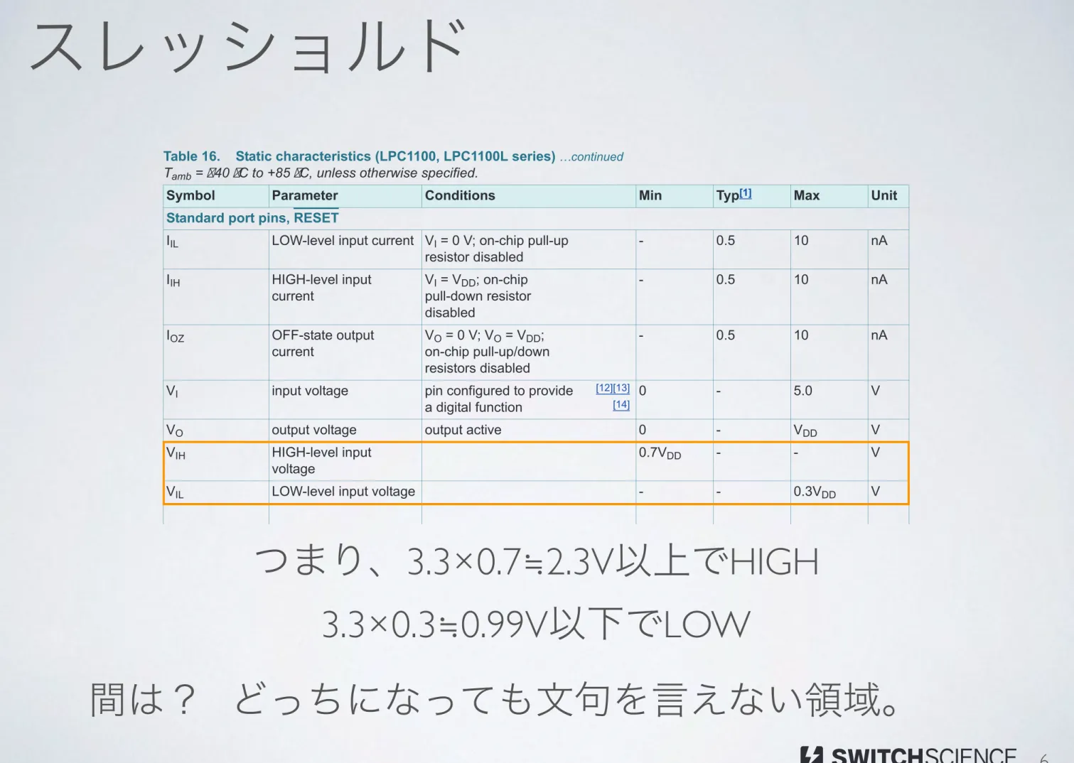
スレッショルド
6
Standard port pins, RESET
I
ILLOW-level input current V
I= 0 V; on-chip pull-up
resistor disabled
-
0.5
10
nA
I
IHHIGH-level input
current
V
I= V
DD; on-chip
pull-down resistor
disabled
-
0.5
10
nA
I
OZOFF-state output
current
V
O= 0 V; V
O= V
DD;
on-chip pull-up/down
resistors disabled
-
0.5
10
nA
V
Iinput voltage
pin configured to provide
a digital function
[12][13] [14]
0
-
5.0
V
V
Ooutput voltage
output active
0
-
V
DDV
V
IHHIGH-level input
voltage
0.7V
DD-
-
V
V
ILLOW-level input voltage
-
-
0.3V
DDV
Table 16.
Static characteristics (LPC1100, LPC1100L series)
…continuedT
amb= 40 C to +85 C, unless otherwise specified.
Symbol
Parameter
Conditions
Min
Typ
[1]Max
Unit
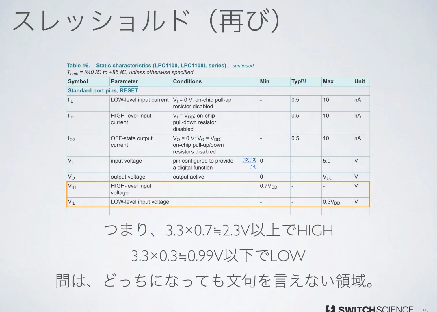
つまり、
3.3×0.7≒2.3V以上でHIGH
3.3×0.3≒0.99V以下でLOW
マイコンの入力
マイコンの入力
酸化絶縁層
MOSFETのしくみ
8
ゲート
ソース
ドレイン
P 型
N 型
N 型
M
etal( アルミ電極 )
O
xide( 酸化絶縁膜 )
S
emiconductor( 半導体 )
ゲート(+)
ソース
ドレイン
P 型
N 型
N 型
+ ー ー ー + +ゲートに電圧が
かかっていないとき
ゲートに電圧が
かかっているとき
FETの回路記号
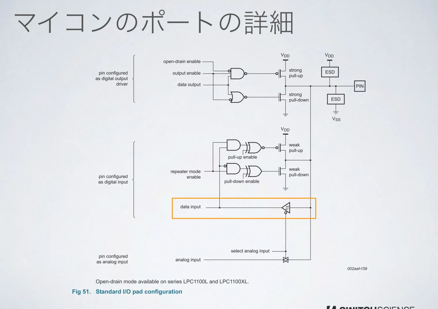
マイコンのポートの詳細
Open-drain mode available on series LPC1100L and LPC1100XL.
Fig 51. Standard I/O pad configuration
PIN VDD VDD ESD VSS ESD strong pull-up strong pull-down VDD weak pull-up weak pull-down open-drain enable output enable repeater mode enable pull-up enable pull-down enable data output data input analog input
select analog input
002aah159 pin configured as digital output driver pin configured as digital input pin configured as analog input
ノイズノイズノイズ
10
1.0V
2.3V
5.0V
きっちりプルアップ/プルダウン
マイコンの入力
こうすりゃいいじゃん?
12
マイコンの入力
こうすりゃいいじゃん?
マイコンの入力
ショート!!
オームの法則
14
マイコンの入力
10kΩ
3.3V
3.3÷(10×10^3)
=3.3×10^-4
=0.00033(A)
=0.33(mA)
しか流れない。
Low
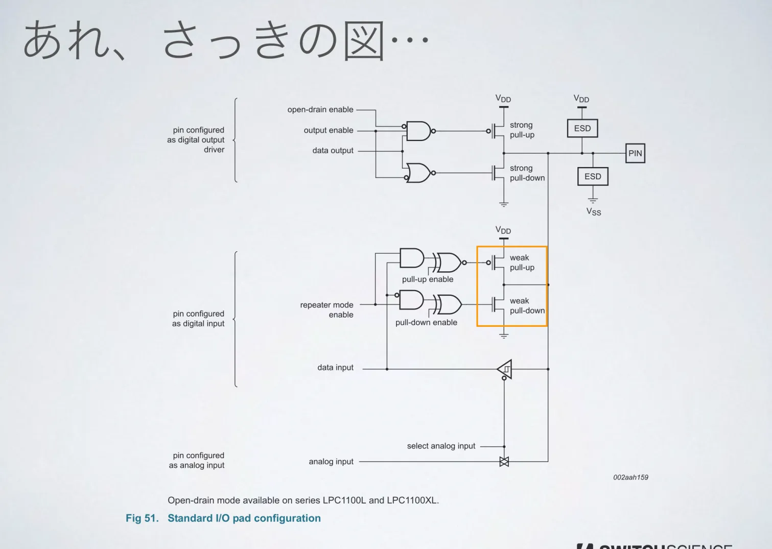
あれ、さっきの図…
Open-drain mode available on series LPC1100L and LPC1100XL.
Fig 51. Standard I/O pad configuration
PIN VDD VDD ESD VSS ESD strong pull-up strong pull-down VDD weak pull-up weak pull-down open-drain enable output enable repeater mode enable pull-up enable pull-down enable data output data input analog input
select analog input
002aah159 pin configured as digital output driver pin configured as digital input pin configured as analog input
DigitalIn Class of mbed SDK
プルアップと言えば…
I²C
スライド一枚でなんとなく分かるI²C
SDA
SCL
GND
SDA SCL GND
SDA SCL GND
SDA SCL GND
マスタ
スレーブ
0b1001000
0b
0
1001000=0x48 Arduino式
0b1001000
0
=0x90 mbed式
0x90
0x98
0xAA
プルアップ抵抗
オープンドレイン
Sm 100kHz
Fm 400kHz(Push-Pull)
Hs 3.4MHz
オープンドレインってなんじゃらほい
20
マイコンの出力
プッシュプル
マイコンの出力
オープンドレイン
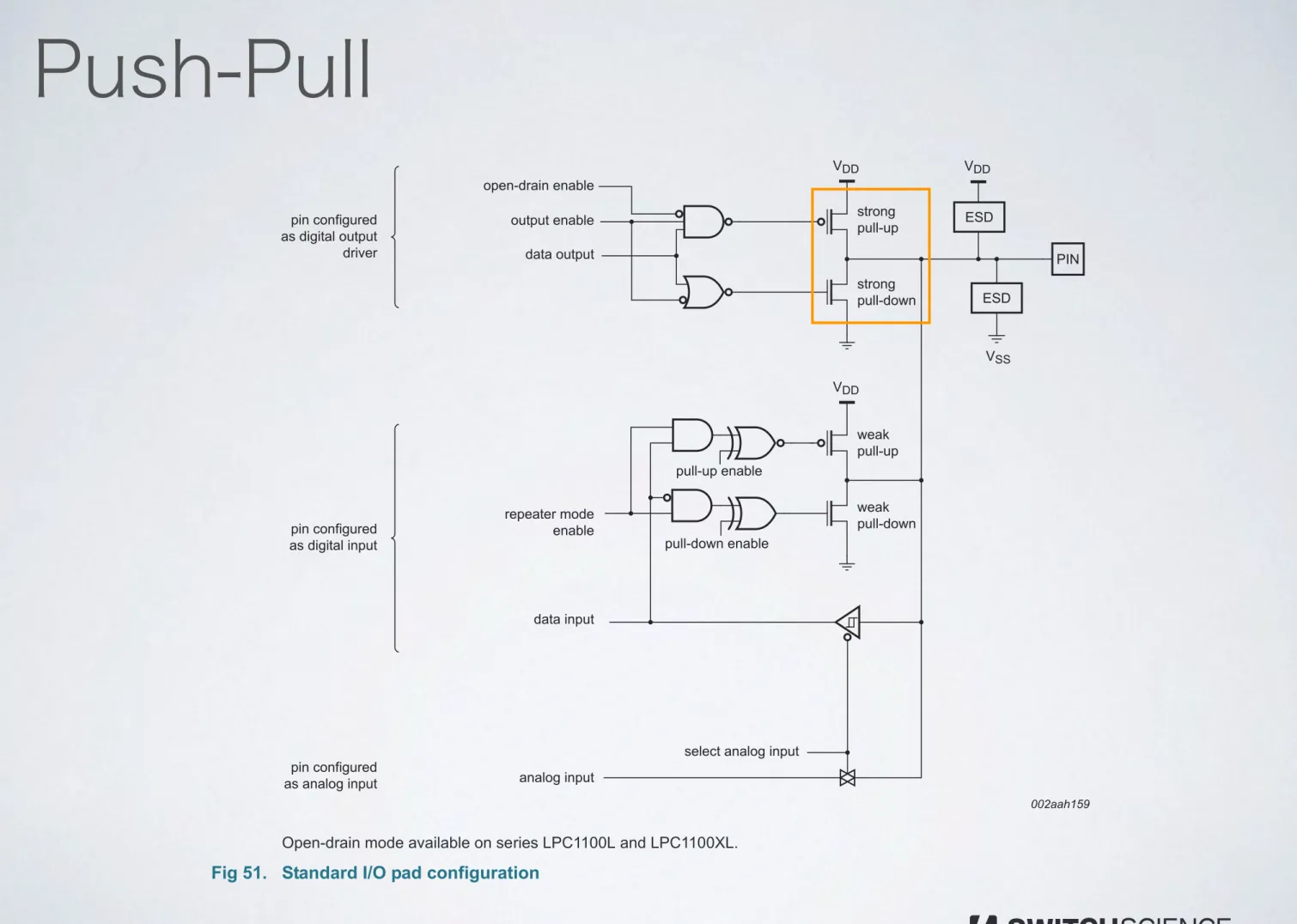
Push-Pull
Open-drain mode available on series LPC1100L and LPC1100XL.
Fig 51. Standard I/O pad configuration
PIN VDD VDD ESD VSS ESD strong pull-up strong pull-down VDD weak pull-up weak pull-down open-drain enable output enable repeater mode enable pull-up enable pull-down enable data output data input analog input
select analog input
002aah159 pin configured as digital output driver pin configured as digital input pin configured as analog input
なぜオープンドレインなのか(1)
22
ショート!!
バスに複数のデバイスが接続されていて、一方で
HIGH、
もう一方で
LOWを出力すると、デバイスのI/Oに過大な
電流を流してしまい、破損につながる。
プッシュプル
なぜオープンドレインなのか(2)
プルアップ抵抗を通るので、過大な電流は流れない。
複数のデバイスが
LOWにしても大丈夫。
(ワイヤード
AND接続)
プルアップ抵抗値が小さすぎると…
24
電圧が
大きく下がっている
下がりきっていない
電圧が下がっているものは、電流を引き込む能力の高い
Fm+対応のスレーブが出している信号。
電圧が下がりきっていないものは、引き込む能力の低い
Fm対応のマスタが出している信号。
スレッショルド(再び)
Standard port pins, RESET
I
ILLOW-level input current V
I= 0 V; on-chip pull-up
resistor disabled
-
0.5
10
nA
I
IHHIGH-level input
current
V
I= V
DD; on-chip
pull-down resistor
disabled
-
0.5
10
nA
I
OZOFF-state output
current
V
O= 0 V; V
O= V
DD;
on-chip pull-up/down
resistors disabled
-
0.5
10
nA
V
Iinput voltage
pin configured to provide
a digital function
[12][13] [14]