Interface and Structural Engineering of
Dye-Sensitized Solar Cells and Perovskite Solar Cells
for High Efficiencies
Galhenage Asha Sewvandi
Japan
September 2015
I
Contents
CHAPTER I
General Introduction ...1
1.1. Evolution of Solar Cell Technology ··· 2
1.2. Basic Solar Cell Characteristic Parameters ··· 4
1.3. Dye-sensitized Solar Cells (DSSCs)··· 6
1.3.1. Structure and Working Mechanism of DSSCs ··· 6
1.3.2. TiO2 Nanostructured Electrodes··· 9
1.3.3. Photosensitizers (Dyes) ··· 12
1.3.3.1. Metal Complex Photosensitizer ... 12
1.3.3.2. Metal- free Photosensitizers... 13
1.3.4. Redox Electrolytes and Counter Electrodes ··· 15
1.3.5. Dye Adsorption Characteristics and Intermolecular Interactions Effect on DSSCs Performances ··· 15
1.3.6. Equivalent Circuit Model of DSSCs ··· 16
1.4. Perovskite Solar Cells (PSCs) ··· 19
1.4.1. Structure and Working Mechanism of PSCs··· 19
1.4.2. Organic-inorganic Metal Halide Perovskite Light Absorbers ··· 22
1.4.3. n-type Semiconductor Electrode ··· 24
1.4.4. Hole Transporting Material (HTM) and Counter Electrode ··· 26
1.4.5. Equivalent Circuit Model of PSCs··· 27
1.4.6. Ferroelectricity and Ferroelectric Solar Cells (FESCs)··· 28
1.5. Purpose of Present Study··· 31
1.6. References··· 34
CHAPTER II Modification of TiO2 Electrode with Organic Silane Interposed Layer for High Performance of Dye Sensitized Solar Cells ...45
2.1. Introduction ··· 45
II
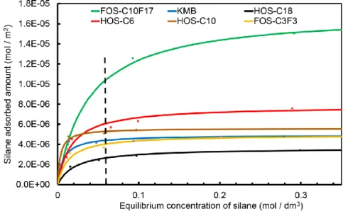
2.2.1. Silane Adsorption on TiO2 Nanoparticles ··· 47
2.2.2. Fabrication of TiO2 Electrode··· 48
2.2.3. Dye and Silane Adsorptions on TiO2 Electrode ··· 48
2.2.4. Fabrication of DSSC ··· 48
2.2.5. Adsorption of N719 Dye on TiO2 Nanoparticles ··· 48
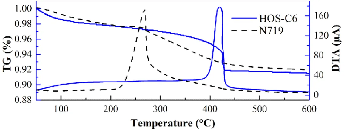
2.2.6. Characterization ··· 49
2.3. Results and Discussion ··· 50
2.3.1. Adsorption of Organic Silanes on TiO2 Nanoparticles ··· 50
2.3.3. Adsorption of Organic Silane on Dye-sensitized TiO2 Electrodes ··· 55
2.3.4. Effect of Silanization-Process Sequence ··· 59
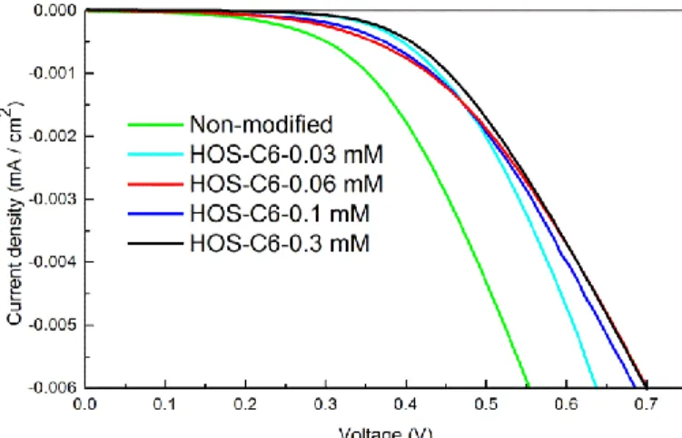
2.3.5. DSSC Performance Modified with Different Type of Silanes ··· 61
2.4. Conclusion ··· 65
2.5. References··· 65
CHAPTER III Inte rplay between Dye Coverage and Photovoltaic Performances of Dye -Sensitized Solar Cells Based on Organic Dyes ...69
3.1. Introduction ··· 69
3.2. Experimental Section ··· 71
3.2.1. Chemicals and Reagents ··· 71
3.2.2. MK-2 dye Adsorption on TiO2 Nanoparticles ··· 72
3.2.3. Fabrication of DSSC ··· 72
3.2.4. Characterization ··· 73
3.3. Results and Discussion ··· 74
3.3.1. Characterization of TiO2 nanoparticles ··· 74
3.3.2. MK-2 dye Adsorption on TiO2 Nanocrystals ··· 76
3.3.3. Current – Voltage Characteristic Curves··· 79
3.3.4. Electrochemical Impedance Characteristic Curves··· 85
3.4. Conclusion ··· 88
III
CHAPTER IV
Organic-Molecules-Modified TiO2 Nanoparticles to Improve Dispersibility of TiO2 Paste
for Enhanced Dye-Sensitized Solar Cells Pe rformances ...94
4.1. Introduction ··· 94
4.2. Experimental Section ··· 96
4.2.1. Solvothermal treatment of TiO2 nanoparticles ··· 96
4.2.2. Synthesis of TiO2 particles for light scattering layer ··· 97
4.2.3. Fabrication of DSSC ··· 97
4.2.4. Characterization ··· 98
4.3. Results and Discussion ··· 98
4.3.1. Adsorption of organic-molecules onto TiO2 nanoparticles surfaces ··· 98
4.3.2. Nanostructure of modified-TiO2 nanoparticles with organic molecules ··· 100
4.3.3. TiO2 particle-size distribution··· 102
4.3.4. Effect of TiO2 nanoparticle dispersibility on DSSCs performances ··· 104
4.4. Conclusion ··· 109
4.5. References··· 110
CHAPTER V Comprehensive Elucidation of Ferroelectric Charge -Separation Effect on Carrie r-Transfer Mechanism in Perovskite Solar Cells ...113
5.1. Introduction ··· 113
5.2. Experimental Section ··· 115
5.2.1. Chemicals and Reagents ··· 115
5.2.2. Synthesis of MAPbI3 powder ··· 115
5.2.3. Fabrication of MAPbI3 pellets ··· 116
5.2.4. Characterization ··· 116
5.3. Results and Discussion ··· 116
5.3.1. MAPbI3 crystal structural analysis··· 116
5.3.2. Ferroelectric characterization of MAPbI3 ··· 118
5.3.3. Dielectric characterization of MAPbI3 ··· 121
IV
5.3.5. Ferroelectric contributions to energy band bending and carrier diffusion length ··· 124
5.3.6. Ferroelectric contribution to I-V hysteresis ··· 127
5.3.7. Strategies to fabricate high performance PSCs ··· 128
5.4. Conclusion ··· 129 5.5. References··· 130 CHAPTER VI Summary...134 Publications··· 139 Acknowledgment··· 141
1
CHAPTER I
General Introduction
The development of clean and sustainable energy is one of the critical issues in the world. A great portion of current energy demand (>85%) is fulfilled by fossil fuel-based resources, causing global warming and consequent severe changes in climate.1
Depletion of fossil fuels, the ever-increasing world energy demand, and greenhouse gases create scientific and technological challenges for the sustainable energy generations. Renewable energy sources (solar, wind, biomass, etc.) derived energy from natural resources that replenish themselves over a period of time without depleting the resources of earth and they have the potential to produce electricity with eliminating the environmental impacts associated with the use of fossil fuels.2 Most
importantly, they generate electricity without producing CO2, the leading cause of
global climate change.
Among renewable energy sources, solar energy; cost effective, abundant in nature, and evenly distributed across the globe, has the potential to cover the world energy demand by itself, which would require covering less than 0.4% of our planet surface with 15% efficient solar panels.3 Solar cell technology can be divided into three
generations: (1) first crystalline silicon solar cells; (2) second generation-thin film solar cells, including a-Si:H, CdTe, CuInGaSe2, etc.; and (3) third
generation-organic and cluster absorber solar cells, including organic thin film solar cells, dye-sensitized solar cells (DSSCs), quantum dot solar cells, and the recently-developed organic-inorganic hybrid perovskite solar cells (PSCs). Commercial modules of silicon-based solar cells with efficiencies (η) of up to ~20% and thin film solar cells with η~15% are available.1 Despite the rapidly increasing global
installations, many of the first and second generation solar cells still suffer from drawbacks such as long payback, relatively high costs associated with the extreme purity requirement for the active material, scarcity of materials such as indium and silver, and low working capability in cloudy conditions or shaded regions.1,4
To resolve many of the issues of the first two generations the third generation solar cells of DSSCs and PSCs have attracted great interest of the researchers due to their
2
low-cost potentials and facile manufacturing methods.4-7 Although, DSSCs suffer
from low efficiencies (~13%)7, DSSC module cost can be further reduced (0.4 $/W p)
by enhancing η up to about 15%.1,8 On the other hand, PSCs as a novel generation of
solar cells have competitive efficiencies (20.1%)9 to market available Si-solar cells,
but its mysterious working mechanism severely hampers further improvements of the materials and device structures for the future developments.
This chapter is organized as follows. Section 1 outlines the evolution of solar cells. Section 2 elaborates basic solar cell characterization parameters. Section 3 discusses the working principle and various components of DSSCs. Section 4 presents the working principle and various components of PSCs; in addition, brief introductions about ferroelectricity and ferroelectric solar cells (FESCs) are included. Section 5 describes the purpose of this dissertation.
1.1. Evolution of Solar Cell Technology
The photovoltaic effect was discovered in the 19th century by Edmond Becquerel.
Solar cell technology can be divided into three types; namely, the first generations, the second generation, and the third generation as illustrated in Figure1.1.This categorization primarily based on the light absorbing material and the manufacturing technology.
3
The first generation solar cells; thus, monocrystalline or polycrystalline solar cells based on silicon wafers, currently dominate the photovoltaic market. Monocrystalline solar cells are manufactured by slicing single crystal ingots, produced by the Czochralski (CZ) method, into wafers of about 200-400 µm in thickness, too thin wafers will break in the slicing and subsequent processing. The high uniformity of the single-crystalline silicon results high-energy conversion efficiencies in monocrystalline solar cells (15-20%).1,10 The high- manufacturing cost and the
material cost due to the production of high-purity Si and thickness limitation are the main weakness of this type of solar cells. On the other hand, polycrystalline solar cells are produced by slicing blocks of cast polycrystalline silicon into thin wafers. Compared to single-crystalline silicon, polycrystalline silicon material is stronger and can be cut into one-third the thickness of the single-crystal material. Polycrystalline solar cells are less efficient (10–14%) than the monocrystalline silicon solar cells due to the hindrance of electrons transfer trough the grain boundaries of small grains.10
The second generation of solar cells is based on thin film materials, and manufactured by depositing a thin film material such as amorphous silicon (a-Si), cadmium telluride (CdTe), and copper indium gallium selenide (CIGS) on a low-cost substrate, steel, glass, or plastic. A thin layer of about 1-10μm can be used due to high absorptivity of the materials (CdTe, CIGS, and a-Si). The less material is required for the thin films; therefore, the total material costs and manufacturing costs are lower than those of the first generations. Despite the promising economic advantages, low cell energy conversion efficiency (5–9% from a-Si and CdTe based cells), and poor stability are the main drawbacks.10-13 However, research results have shown the
highest energy conversion efficiency of 22% with CIGS thin film solar cells.9,12 Even
though, CIGS cells have high efficiency and stability, its unresolved issues relating to high cost of manufacturing and expensive rare-metal of In and Ga are the limitations.
Unlike the first and second generation solar cells, which require clean rooms and vacuum-based device fabrication facilities, third- generation solar cells can be manufactured using solution-based, low-temperature roll-to-roll manufacturing methods.1 Among the various types of third generation solar cells, DSSCs are
promising due to their low-cost fabrication together with positive inherent features such as workability under low- light conditions, ability to generate energy at any incident angles of light, flexibility, and transparency.1 These exclusive features of
4
DSSCs not only increases their operating hours, but also allow them to be deployed in shaded regions, corners or bends in buildings.
A breakthrough in the third generation solar cells is the emergence of perovskite solar cells (PSCs), which employ an organic–inorganic hybrid perovskite absorber (commonly CH3NH3PbX3, X = Br, Cl, or I).14-17 Competitive efficiencies (20.1%)9 to
market available Si-solar cells have been reported in PSCs, which represents a fivefold improvement in just five years since the first report.6 Nevertheless, the
replacement of lead (Pb) with some non-toxic material may presumably increase their market acceptability.
1.2.Basic Solar Cell Characteristic Parameters
The current-voltage characteristic curves or simply I-V curves of the electrical devices are a set of graphical curves which are used to define its operation within an electrical circuit. As its name suggests, I-V characteristic curves show the relationship between the current flowing through the device with the applied volt age across the device. A typical I-V characteristic curve of a solar cell is illustrated in Figure 1.2.
Figure 1.2. The typical I-V characteristic curve of a solar cell
At any operating points the electrical power generated by the cell is given by the J*V product. The short-circuit photocurrent density (Jsc), open-circuit photovoltage
5
photovoltaic characteristic parameters used in solar cell characterizations, which can be extracted from the I-V curves. The Jsc is a current density without any external
applied voltage; namely, current density in the short circuited solar cell. The Voc is a
voltage in the open circuited solar cell; thus, no current flowing between the anode and the cathode. The theoretical maximum Voc value of the DSSC is the difference
between Fermi level of the n-type semiconductor and the redox potential of electrolyte, and the theoretical maximum Voc value of the perovskite solar cells (PSC)
is the difference between Fermi levels of the n-type semiconductor and the HOMO level of hole transporting material. The ideally shaped I-V characteristic would be rectangular and would deliver a constant current density of Jsc until reaching the Voc
(Figure 1.2). For such characteristic the maximum power point would have a current density of Jsc and a voltage of Voc. The term called fill factor (FF) has been invented
to measure how close a given characteristic is to conforming to the ideal rectangular J-V shape. Thus, it provides the deviation of the cell performances to the theoretical maximum performance. The fill factor is given by;
1 ; FF V J V J FF oc sc mp mp (1.1) where Jmp and Vmp are the current density and voltage at the maximum power point,
respectively.
The standard power conversion efficiency (η) of solar cells is evaluated by measuring the power produces under 1 sun illumination (illumination at 1.5 AM, 100 mW/cm2). And it can be calculated by equation 1.2.
ph
oc
sc
V FF I J / (1.2) Therefore, improvement of the power conversion efficiency (η) of solar cells means enhancements of the cell characteristic parameters of short-circuit photocurrent density (Jsc), open-circuit photovoltage (Voc), and fill factor (ff).6
1.3.Dye-sensitized Solar Cells (DSSCs)
The DSSC is a photoelectrochemical device in which the photocurrent is generated at an interface between a dye-anchored metal oxide semiconductor and a hole-conducting electrolyte upon light absorption.1 Since the initial work by Grätzel and
coworkers in 1991,18 DSSCs have attracted scientific interest due to their low cost
energy generation potential. As a next generation of solar cells, DSSCs have several advantages over silicon-based solar cells such as the ability to maintain generation characteristics even in a weak light condition as well as at any incident angle, and the ability to use a variety of designs and colors. DSSCs also have a high potential to expand the range of use of solar cells including variety of consumer-related applications in which conventional solar cells are unfit. It has also been reported that the major contribution (50–60%) to the manufacturing cost of DSSC modules arises primarily from dyes, electrolytes, and substrates.19-21 The materials to enhance the
efficiency and to reduce the cost of DSSCs are widely investigated.18-26
1.3.1. Structure and Working Mechanism of DSSCs
A typical DSSC consist of a transparent conductive substrate ( fluorine-doped tin oxide (FTO)), a high surface area n-type semiconductor (usually TiO2), a dye
(sensitizer) which absorbs light, an elec trolyte containing a redox mediator, and a counter electrode.19 A schematic structure of a typical DSSC is shown in Figure 1.3.
7
The dye-sensitized TiO2 photoelectrode is prepared by coating mesoporous
nanostructured TiO2 layers on the FTO conducting glass surface, and adsorbing
sensitizer dye molecules on the TiO2 nanoparticles surface. The counter electrode is
fabricated by depositing Pt catalyst on the FTO conducting glass surface. The photoelectrode and Pt counter electrode are assembled into a sandwich-type cell and a drop of redox electrolyte solution is injected in between them to comp lete the cell. The basic charge transfer processes in a DSSC are shown in Figure 1.4. In DSSCs other than the effective photogenerated charge transfer processes photogenerated charge loss processes may also occur.
Figure 1.4. Systematic of electron transfer pathways in a dye sensitized solar cell
In Figure 1.4, the desired working mechanism of a DSSC is indicated by red arrows and the reaction mechanism can be explained as follows:27
(1) Excitation process; the electrons in photosensitizers are excited from the HOMO (highest occupied molecular orbital) level, S, to the LUMO (lowest unoccupied molecular orbital) level, S*, upon absorption of photons from incident light.
𝑆 + ℎ𝑣 → 𝑆∗ (1.3)
(2) Injection process; the excited dye molecules inject excited electrons from LUMO into the conduction band of the TiO2 photoelectrode while oxidizing the dye (S+).
8
𝑆∗ → 𝑒−(𝑇𝑖𝑂
2) + 𝑆+ (1.4)
(3) Energy generation; the injected electrons transfer through the TiO2 nanoparticles
with diffusion toward the FTO and consequently generating energy while the electrons flow through the outer electrical circuit to the counter electrode (C.E.). 𝑒−(𝑇𝑖𝑂
2) → 𝑒−(𝐶. 𝐸. ) + 𝑒𝑙𝑒𝑐𝑡𝑟𝑖𝑐𝑎𝑙 𝑒𝑛𝑒𝑟𝑔𝑦 (1.5)
(4) Regeneration of the mediator; the oxidized I3- ions diffuse toward the counter
electrode and they are reduced back to I- ions.
2𝑒−(𝐶. 𝐸. ) + 𝐼
3−→ 3𝐼− (1.6)
(5) Regeneration of the dye; the oxidized dye (S+) is regenerated by accepting
electrons from the I- ions in the electrolyte followed by oxidation of the I- ions into the
I3- ions.
2𝑆++ 3𝐼−→ 2𝑆 + 𝐼
3− (1.7)
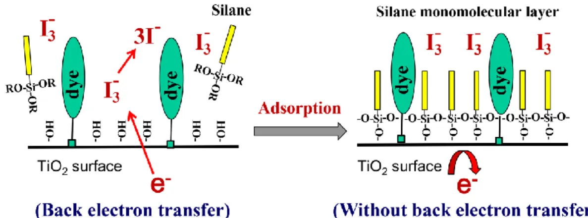
In Figure 1.4 the loss reactions 6, 7, 8, and 9 are indicated in blue. Reaction 6 is direct recombination of the excited electron and hole in the dye molecule reflected by the excited state lifetime. Recombination of injected electrons in the TiO2 with either
acceptors in the electrolyte or oxidized dyes is numbered as 7 a nd 8, respectively. In principle, electron transfer to I3- can occur either at the interface between the
nanocrystalline oxide and the electrolyte, 7, or at areas of the anode contact (usually a fluorine-doped tin oxide layer on glass) that are exposed to the electrolyte, 9. These back-electron transfer processes diminish the DSSC performance.24,28,29 In practice,
the route 9 can be suppressed by using a compact blocking layer of oxide deposited on the anode by spray pyrolysis.23,24The back electron transfer on the TiO
2 surface is
much higher than that on the FTO surface because of the large surface area of TiO2
exposed to the electrolyte solution.22Extensive studies on minimizing the back
electron transfer, injected electrons in the TiO2 with acceptors in the electrolyte (7),
have been reported. The addition of additives to redox electrolyte, such as 4-tert-butylpyridine (TBP) and guanidinium thiocyanate (GuSCN), have suppressed the back-electron transfer by adsorbing these additives on the surface of the TiO2
electrode; thus, blocking reaching of I3- ions to the TiO2 surface.29-31 Although TBP
9
decreases the electron injection yield (Jsc) due to the risen conduction band edge of the
semiconductor close to the LUMO of the dye molecules.28 Moreover, these cations
formed weak bonds on the TiO2 surface. Therefore, it is vital to investigate stronger
surface modification techniques for high-efficiencies.
The positions of the energy leve ls at the oxide/dye/electrolyte interface are fundamentally important to the function of the DSSC. The performance of a DSSC is basically based on four energy levels; namely, (1) the LUMO level of dye, (2) the HOMO level of dye, (3) the Fermi level of TiO2 electrode, and (4) the redox potential
of electrolyte. The small energy separation between the HOMO and LUMO ensures absorption of low energy photons in the solar spectrum; thus, the photo-generated current density, Jsc, generated from the DSSC is depende nt on the HOMO-LUMO
levels separation.27 The energy level of the LUMO must be sufficiently negative for
the effective injection of electrons and the HOMO level must be more positive to the redox potential of the electrolyte for the fast regeneration of dye. The maximum voltage generated by the cell, Voc, corresponds to the energy difference between the
Fermi level and the redox potential of electrolyte.27
1.3.2. TiO2 Nanostructured Electrodes
Mesoporous nanostructured metal oxide film is a critical compone nt, in terms of creating transport path ways for photo-generated electrons, providing high surface areas for the adsorption of dyes, and providing pores for the electrolyte solution to permeate.27,32 Titanium dioxide has been attracted as a promising mater ial for the
mesoporous film due to the high charge collection efficiency and electron transportation by the well-connected internal network structure, good stability in solution under irradiation, non-toxicity, and cheap availability.27,32 Even though many
other simple and ternary n-type metal oxide semiconductors such as ZnO, SnO2,
Nb2O5, SrTiO3 and Zn2SnO4, as well as core-shell structures, ZnO-coated SnO2,have
been investigated.33-35
The nanostructured electrode usually consisting of a ∼10 μm thick film of mesoporous TiO2 with ∼20 nm particle size to provide a large surface area for
sensitizer adsorption and good electron transport to the substrate.32,36 Several crystal
10
thermodynamically most stable form with higher mass density, refractive index, and dielectric constant than that of anatase. Anatase is a metastable phase which transforms to rutile above 600 °C. Nevertheless, the preferred structure in DSSCs is anatase because it has a larger bandgap (3.2 vs 3.0 eV for rutile) and higher conduction band edge energy, Ec. This leads to a higher Fermi level and Voc in
DSSCs.37,38
The facet exposed on the TiO2 nanocrystal surface greatly affects the DSSC
performance due to the different surface energies of the different facets which effects on the dye adsorption density and dye adsorption constant.39-42 The strong adsorption
of the dye molecules onto the high-energy facets enhance η by effective injection of photogenerated electrons from the dye molecules into the conduction band of TiO2.40
One of the important factors that affect the cell efficiency is the thickness of the nanostructured TiO2 layer. Although thick films provide high surface areas for the
high-adsorption of dyes (higher LHE, light harvesting efficiency), the dark current, loss of electrons, is increased as electrons have to be travelled through increased number of nanoparticles and grain boundaries.
A film consists of large TiO2 particles (250–300nm) can be used as a scattering
layer for incident photons to improve the LHE by increasing the absorption path-length of photons.43-47 In this case, the photo-electrode is comprised of nanostructured
TiO2 layer and light scattering layer of the large TiO2 particles, a double layer
structure, as shown in Figure 1.5. By using the light scattering layer, the thickness of nanostructured TiO2 layer can also be reduced; which reduces resistance for the
electron transportation across the mesoporous layer to the FTO glass and improves the utilization of photogenerated electrons.36 Various types of scattering layers such as
11
Figure 1.5. Effective light harvesting by light scattering layers: (a) single layer structure; (b)
double layer structure
The porosity of the TiO2 film is also important because the electrolyte, which
contains the redox ions, must be able to penetrate the film effectively. Appropriate porosity of 50–70% is controlled in the sintering process by addition of a polymer such as polyethylene glycol (PEG) and ethyl cellulose (EC) into the TiO2 paste.48
DSSCs performances can be further enhanced by properly controlling photo-electrodes properties.
The TiO2 nanostructured electrode is prepared by coating TiO2 paste on a FTO
substrate using doctor blade or screen printing techniques and then sintering at about 450–500°C.23,48 High efficiencies can be achieved by annealing at high temperatures
as a result of the reduced electron transport resistance of TiO2 film by well-connected
TiO2 particles; however, at high temperatures conductivity of the FTO can be
dropped49 and differences in the thermal expansion coefficients of TiO
2 and FTO can
cause the TiO2 film to detach from the FTO surface.50
On the other hand, although the primary size of TiO2 nanoparticles use in the TiO2
paste is about 20 nm, the high surface energy of nanoparticles causes them to agglomerate in the synthesis processes. This leads to materials with primary particles in the nanometer range with variable and complex networks, shapes, and morphologies in a paste51 which is used for the TiO
2 electrode preparation. The actual
morphology variation with the synthesis process can have large batch-to-batch variations leading to poor reproducible performances in long-term experiments.50,51
On the other hand, the presence of large aggregates in the paste as a result of the poor dispersion of the TiO2 nanoparticles leads to a non-uniform nanostructured
12
sometimes it leaves small cracks in the TiO2 film after sintering.50 Therefore, highly
dispersed of TiO2 nanoparticle paste is necessary to fabricate uniform nanostructured
TiO2 films for DSSCs.
1.3.3. Photosensitizers (Dyes)
A sensitizer dye, one of the crucial parts in the DSSC, anchored to the surface of TiO2 nanocrystals absorbs the solar radiation and transfers the photo-excited electron
to the conduction band of the TiO2. Other than the energy levels alignments as
discussed in the section 1.3.1, the sensitizer should have characteristics such as (1) anchoring groups (-COOH, -H2PO3, -SO3H, etc.) to strongly bind the dye onto the
semiconductor surface, (2) the whole visible region and even the part of the near-infrared (NIR) covered absorption spectrum, (3) unfavorable dye aggregation avoided dye molecular structures, (4) photo-stability, electrochemical stability and thermal stability.29 Based on these requirements, many different photosensitizers including
metal complexes52,53 and metal- free organic dyes54-68 have been extensively
investigated for DSSCs.
1.3.3.1. Metal Complex Photosensitizers
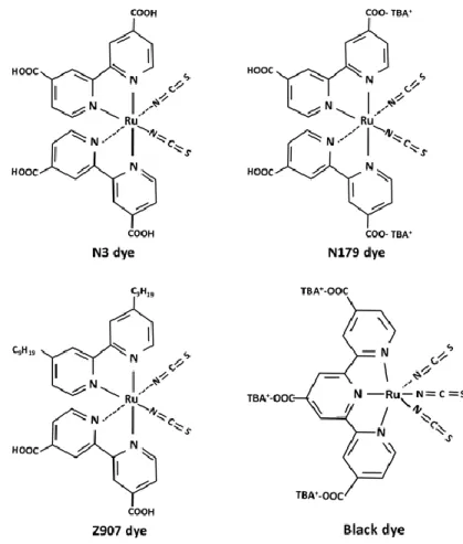
Generally, metal complex photosensitizers consist of a central metal ion with ancillary ligands having at least one anchoring group. Anchoring groups are employed to link the dye with the semiconductor and facilitate the injection of the excited electron into the CB of the semiconductor. Light absorption in the visible part of the solar spectrum is due to a metal to ligand charge transfer (MLCT) process. The central metal ion is therefore a crucial part of the overall properties of the complexes. Among the metal complexes such as ruthenium (Ru(II)), osmium (Os(II)), Re (I), Fe (II), Cu(I) complexes; Ru(II) complexes have shown the best photovoltaic performances and are generally used in DSSCs. Most well-known Ru complexes for DSSCs are shown in Figure 1.6; namely, N3, N719, Z907, and black dye (N749).56 The high
efficiencies of the DSSCs based on Ru-complexes can be attributed to their wide absorption range from the visible to near- infrared regime due to loosely attached thiocyanate (NCS) ligands, which rise the HOMO energy of the complex; nevertheless, NCS is the weakest part of Ru complex from a chemical stabilit y point
13
of view.27 In addition, the carboxylate groups attached to the bipyridyl moiety lower
the energy of the ligand π* orbital. Because the electronic transition is the MLCT, excitation energy is effectively channeled to the carboxylate group, from whic h electron injection into the conduction band of TiO2. However, the molecular
extinction coefficients of these metal complex dyes are moderate (ε ≤ 20,000 L mol -1).56 The low-absorption coefficients require thicker TiO
2 electrodes to absorb more
dyes. The increase of the thickness has disadvantages in view of electron transport and open circuit voltage; thus, Jsc and Voc could decrease.
Figure 1.6. Structures of Ruthenium (II) complexes used in dye-sensitized solar cells
1.3.3.2. Metal-free Photosensitizers
Compared with metal- free organic dyes, ruthenium- complex dyes are delivering DSSCs with high-photoenergy-conversion efficiencies. But, it contains expensive rare- metal of ruthenium and it requires tricky purification steps.56 On the other hand,
metal- free organic dyes can be prepared rather inexpensively by established synthesis strategies. The major advantages of the metal- free organic dyes are their large
14
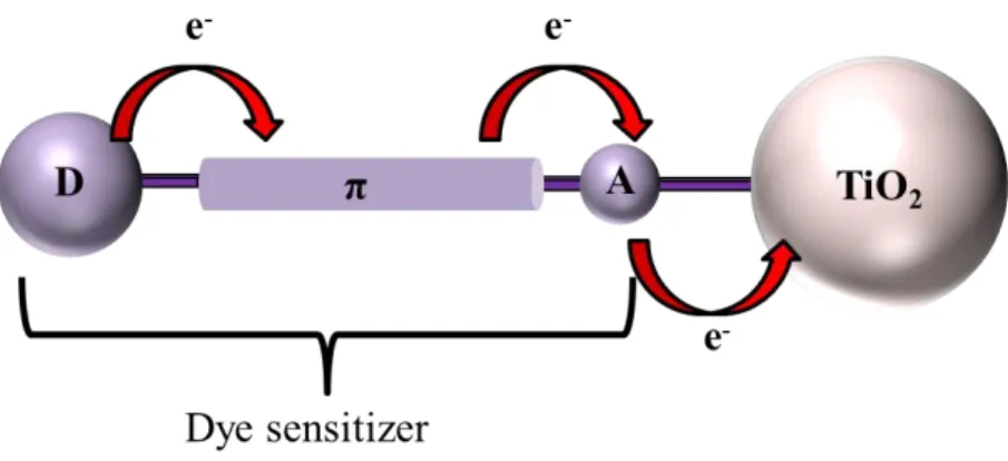
absorption coefficient, low cost, availability, and facile manufacturing. Generally, the structure of metal- free organic dye consists of a donor group, a π-conjugation linkage, and an acceptor group as shown in Figure 1.7.This construction gives excited electrons with long lifetimes due to an effective intramolecular charge separation. Upon solar radiation an electron is excited from the HOMO level, which is located on the electron rich donor part (D), to the LUMO level on acceptor group (A) through the π-conjugation linkage. The excited dye injects the electron into the CB of TiO2 via the
acceptor group.
Figure 1.7. Schematic drawing of the D-π-A metal-free organic dye structure, D: donor
group; π: π-conjugation linkage; A: acceptor group
Many efforts have been made to change the different parts of organic dyes; namely D, π and A, to optimize the DSSC performance. Dyes with different types of donor groups such as coumarins,54 indoline, carbazole,59,62,66 diphenyaneline,67 and
ullazine68 have been synthesized to obtain high extinction coefficient. Cyanoacetic
moiety57, and rhodanine moiety66 have been used as acceptor groups. The moieties
with thiophene58,59,65 are widely used as a π-conjugated linkage because of their
excellent electron transportation ability. However, strong intermolecular interactions between the dye molecules show high tendency to aggregate when they are adsorbed.69,70 Coadsorbents like cholic acid derivative are commonly employed with
the metal- free organic dyes to abate the strong intermolecular interactions and break up dye aggregations.71,72 The latter, coadsorbents reduce the DSSCs performances by
15
1.3.4. Redox Electrolytes and Counter Electrodes
A redox electrolyte used in the DSSC regenerate oxidized dye molecules and transports electrons between the TiO2 photo-electrode and the counter electrode.
Liquid redox electrolytes, gel and polymer electrolytes, and ionic liquid electrolytes have been employed in DSSCs.31,73,36 Nevertheless, the liquid electrolyte containing I
-/I3- redox couple produce higher conversion efficiencies. Viscosity of the solvents
direct affects the ion conductivity and low-viscosity solvents yield the better performance. The constituents in the electrolyte have an influence on the yield of electron injection, open-circuit voltage, electron diffusion coefficient and the rate of dye cation regeneration.31,73,36
At the counter electrode I3- ions, formed by the reduction of dye cations with I- ion,
are reduced to I- ions. To reduce the I3- ions, the counter electrode must have high
electrocatalytic activity. Pt coated on FTO substrate is usually used as the counter electrode. Carbon materials, conducting polymers, and cobalt sulfide have also been studied as alternatives for the expensive Pt.27,29
1.3.5. Dye Adsorption Characteristics and Intermolecular Interactions Effect on DSSC Performances
The photovoltaic performance of DSSC is highly dependent on the adsorption characteristics; namely, dye adsorption constant (Kad) and dye adsorption density (Q),
of the particular dye used as the sensitizer.40Binding between the dye anchoring gro up
and the semiconductor (TiO2) is paramount important for the effective charge
injection. Dye adsorption constant, which can easily be estimated from the dye-adsorption isotherm, is a primary indicator of the bonding strength. Strong grafting of the dye on to the TiO2 represents by a high Kad value. And Jsc increases with Kad due
to the effective photo-generated electron injection. A high coverage of TiO2 surface
by adsorbed dye (high-Q) inhibits the parasitic back-electron transfer reactions by acting as an insulating layer toward the approach of electrolyte to the TiO2 surface at
the TiO2/electrolyte interface. As a result of reduced charge recombination with
increasing Q increases Voc.40
Dye-dye intermolecular interactions are required to make a compact dye monomolecular layer on the TiO2 surface. Although, the tightly packed
16
monomolecular layer of dye, a high-Q, is desirable for efficient light absorption, strong dye-dye intermolecular interactions have the drawback of introducing undesired effects that may limit the DSSC efficiency. Dye aggregation is known to lead to intermolecular excited-state quenching reducing the DSSCs photocutrrent.71,74,75 Especially, metal- free organic dyes shows π-stacked aggregate
due to strong π-electron interactions.71 Although π-π stacking is advantageous to the
light harvesting, π-stacked aggregate usually leads to inefficient electron injection and thus results in low power conversion efficiency.74 The prohibition of π-π stacking
with additives in the dye solution has been used to improve efficiency of organic dye-sensitized solar cells suffering from the π-π stacking problem. Coadsorption of dye with additives71,74 and structural modification of dye molecules75,54 is proven to be
effective to dissociate π-π stacking or dye aggregation and thus to improve solar cell efficiency. Wang et. al. have reported the reduction of dye loading by about half with the addition of deoxycholic acid (DCA) as a coadsorbent.71 Hara and co-workers have
found that the increasing alkyl-chain length of alkyl- functionalized thiophenes, to reduce intermolecular interactions, decreased the dye adsorption density without lowering electron lifetime.58,62 They suggest that in the terms of electron lifetime, the
important criterion is the dye coverage on TiO2 surface and not the adsorbed
amount.62 Hahlin et.al. have suggested that differences in the dye coverage has a
minor effect on the charge generation from the individual molecules by using core level photoelectron spectroscopic studies.67Computational modeling and theoretical
studies have also suggested the significant degree of excited electron and hole recombination results from strong dye-dye intermolecular interactions at high dye coverage on TiO2 surface will diminish the DSSC performance.70,72 Therefore,
systematic studies on effect of dye coverage on photovoltaic performances are warranted.
1.3.6. Equivalent Circuit Model of DSSCs
Figure 1.8(a) shows the equivalent circuit model representing for the DSSCs, where Rrc and Cµ are resistance associated to the electron-transfer resistance at the
TiO2/electrolyte interface and capacitance of the interface; RD and CD are resistance
17
resistance and capacitance at the P t/electrolyte interface counter electrode; Rs is
attributed to the total series resistance of wiring, FTO, and blocking layers.
Figure 1.8. Impedance spectroscopic analysis of the DSSC: (a) equivalent circuit model; (b)
impedance spectrum
Impedance spectroscopy (IS) is a powerful, versatile technique to study the salient electronic and ionic processes in an electrochemical system. In general, an impedance (Z(ω)) measurement is performed by applying a certain ac voltage, V(ω), to the cell and
measuring the ac electrical current through the cell, I(ω), at a certain angular frequency, ω, or vice versa.
)
(
)
(
I V Z (1.8) Z(ω) = Z′(ω) + Z″(ω) (1.9) Where Z′(ω) and Z″(ω) are real and imaginary components of the impedance, Z(ω),respectively. An impedance spectrum, the result of Z(ω) measurement, relates to the equivalent circuit model of the DSSC as shown in Figure 1.8. During the impedance measurement the cell is kept at a fixed state by imposing stationary constrain such as
18
the dc bias, illumination intensity etc. And the Z(ω) is measured by scanning the frequency (f), typically from mHz to 10 MHz. The resistances and capacitances values in the equivalent circuit model can be evaluated from the impedance spectrum.
In the typical DSSC impedance spectrum (Figure 1.8(b)), the high frequency arc is due to Rpt and Cpt at the Pt counter electrode, the low frequency arc is attributed to RD
and CD of diffusion of redox species in the electrolyte, and the intermediate frequency
arc is attributed to Rrc and Cµ associated to the electron-transfer at the TiO2/electrolyte
interface. The displacement of the arc, Rs, from the origin is attributed to the total
series resistance of wiring, FTO, blocking layers, and porous TiO2 film. TheRrc, RD
and Rpt resistances of DSSCs can be evaluated from the diameter of the corresponding
arcs in the impedance spectrum as shown in Figure 1.8(b). These resistances strongly affect the cell parameters. Jsc and FF are decreased as a consequence of high-Rs due to
the reduced charge collection by the high resistance, the lower Rs is the better. A
high-Voc value can be obtained by enhancing the Rrc value, increasing the resistance to the
charge recombination at the TiO2/electrolyte interface.
The capacitances—Cpt, Cµ, and CD—can be estimated from the equation 1.10 using
the corresponding resistance and the peak frequency of arc as shown in formula (1.10), which presents for the Cµ.76
max 1 rc R C (1.10)
Among these capacitances, Cµ is the most important because it related only to the
variation of the chemical potential in the TiO2; thus, the electron density in the TiO2
electrode is directly proportional to the Cµ value.76,77
Lifetime of an electron, τn, in TiO2 electrode can be determined from the equation
1.11.78 The higher lifetime yields the better performances.
C R
rc
19
1.4.Perovskite Solar Cells (PSCs)
A recent newcomer to the field of solution processed photovoltaics, the third generation, is the lead halide perovskite solar cell. It is based on organic−inorganic light absorbing semiconductor material with a perovskite structure, CH3NH3PbX3,
where X is a halide atom (I, Cl, Br, or a combination of some of them). This light harvester material has recently provoked a major progress starting with the work of Miyasaka et. al. in 20096 who used it as a variant of the DSSC configuration, thus a
nanostructured TiO2 perovskite-sensitized solar cell. Subsequently, the perovskite
solar cells have been assembled in a variety of architectures, either in mesoporous (nano- heterojunction) or planar thin film, and used the perovskites with different chemical compositions and preparation routes. Very quickly; thus, the initial efficiency about 4% (2009) have passed to values about 20%9 (2014)representing a
fivefold improvement in just five years.6 These soaring efficiencies and the cheap
production cost of PSCs have impressed the market as an extremely commercially attractive option.
1.4.1. Structure and Working Mechanism of PSCs
A typical PSC consists of an n-type semiconductor electron transport material, a perovskite light absorber, a hole transporting material, and a counter electrode. A schematic structure of the typical PSC is shown in Figure 1.9. Generally, TiO2 is used
as the n-type semiconductor and Au as the counter electrode.
20
The typical PSC fabrication process commences with the deposition of a compact TiO2 hole-blocking layer on top of the FTO substrate. This is typically done through
the spray pyrolysis of titanium precursors such as titanium diisopropoxide bis(acetylacetonate) at 450 °C. It is important to ensure that the compact layer is pinhole free and uniform to prevent the recombination between photogenerated electrons in FTO and holes in the perovskite layer or HTM layer. On top of the compact layer, a mesoporous layer of n-type TiO2 is formed either by screen printing
or spincoating a nanoparticle TiO2 paste followed by annealing to remove the
polymeric binders to obtain a mesoporous TiO2 n-type semiconductor layer. The
perovskite films are then deposited on top of the n-type mesoporous layer by spincoating its solution in an organic solvent such as γ-butyrolactone (GBL) or N,N-dimethylformamide (DMF). This is followed by the deposition of a hole transporting material (HTM), generally spiro-OMeTAD with appropriate dopants to improve conductivity. Finally, a metal electrode, Au, is deposited on top of the HTM to complete the cell.
The schematic illustration of electron transfer processes and energy levels in the PCS is displayed in Figure1.10.
Figure1.10. Schematic illustration of the electron transfer processes and energy levels in
PCSs
Red arrows (1, 2, and 3) in Figure 1.10a represent the forward charge transfer processes. When the perovskite light absorber in the cell is illuminated subsequently an electron is excited from the valence band (VB) to the conduction band (CB), (1). It has been reported, hybrid organic- inorganic lead halide perovskites do cumulate
CH3NH3PbI3 CB -4.2 ev -5.43 ev VB CB -3.89 ev HOMO -5.22 ev TiO2 Spiro OMeTAD (3) (2) (1) (4) (5) (6) (7) CH3NH3PbI3 CB -4.2 ev -5.43 ev VB CB -3.89 ev HOMO -5.22 ev TiO2 Spiro OMeTAD (3) (2) (1) (4) (5) (6) (7) CH3NH3PbI3 CB -4.2 ev -5.43 ev VB CB -3.89 ev HOMO -5.22 ev TiO2 Spiro OMeTAD (2) (1) (3) (4) (5) (6) (7) -4.2 ev TiO2 -3.8 ev Perovskite -5.4 ev HTM -5.2ev -4.5 ev FTO -5.1ev Au e -h+ h+ e -(a) (b)
21
functions of light absorption, n-type conduction, and p-type conduction.79 Charge
separation can then occur through two possible primary reactions: (2) injection of photogenerated electrons into the conduction band of TiO2 (equation 1.12) and/or (3)
injection of holes into the HOMO of HTM (equation 1.13).
2
( )) ...
(e h perovskitee TiO h perovskite (1.12a)
) ( ) (perovskite h HTM h
(1.12b) and/or
Perovskite
e HTM h perovskite h e... ) ( ) ( (1.13a) ) ( ) (perovskite e TiO2
e
(1.13b)Blue arrows (4, 5, 6, and 7) in Figure 1.10(a) indicate the possible recombination mechanisms of photogenerated electrons and holes;79namely, (4) non-radiative
exciton recombination, (5) back-electron transfer at the TiO2/perovskite interface, (6)
back-electron transfer at the perovskite/HTM interface, and (7) charge recombination at the TiO2/HTM interface through perovskite pinholes. Proper alignment in the
energy levels can minimize these charge recombination mechanisms.
The small energy separation between the VB and CB of the perovskite absorbers ensures absorption of low energy photons in the solar spectrum; thus, Jsc generated
from the PSC is dependent on the VB and CB separation. In the PSC system, energy level of the CB of the perovskite light-absorber must be more negative (higher) than the CB of the n-type conductor (TiO2) for the injection of photogenerated electrons
from the perovskite to the TiO2, and also VB of the perovskite must be more positive
(lower) than the HOMO of HTM for the transfer of photogenerated holes from the perovskite to the HTM (Figure 1.10b). The maximum voltage generated by the cell, Voc, corresponds to the energy difference between the Fermi level of the TiO2 and the
HOMO level of HTM.80 Energy levels for different materials acting as electron
transport materials, absorbers, and hole transporting materials use in solar cells are displayed in Figure 1.10b. Although the structure of PSCs is similar to DSSCs, the working mechanism of PSCs is different from DSSCs due to charge transportand
22
charge accumulation properties in the perovskites.81,82 In DSSCs instantaneous
injection of excited-electrons from the dye into the TiO2 occurs and no charge
accumulation is observable in the light absorber. The electron and hole injection processes and charge separation processes in the PSC system remain unclear.
1.4.2. Organic-inorganic Metal Halide Perovskite Light Absorbers
Organic-inorganic halide perovskites materials have the basic building block with an AMX3 chemical composition, A is a large cation, M is a smaller metal cation, and
X is an anion from the halide series. They form an octahedral structure of MX6, which
forms a three dimensional structure connected at the corners as shown in Figure 1.11. The component A fills the coordinated space between the octahedra that form in these three-dimensional structures. The size of the cation A is an important aspect for the formation of a closed packed perovskite structure, since this cation A must fit into the space comprised of the four adjacent octahedra which are connected together through shared corners. In these organic-inorganic halides, the methylammonium, ethylammonium and formamidinium organic cations are typically used. The metal cations are usually divalent metal ions such as Pb2+, Sn2+, and Ge2+ while the halide
anions are I−, Cl−, and Br−. The optical and electronic properties of the perovskite materials can be tuned to a great extent depending on the size of the metal ion, halide ion, and the organic cation.83
23
Structure and physical properties of the organic- inorganic halide perovskite,
(C4H9NH3)2(CH3NH3)n-1SnnI3n+1, were first reported by Waber in 1978.83 After that,
considerable attention has been paid to its potential of a transition from insulator to metallic conductor by increasing the number of inorganic layers in the organic-inorganic perovskites.84 However, considerable attention has not been paid for the
photovoltaic ability until Miyasaka et. al. used (CH3NH3)PbI3 perovskite nanocrystals
as sensitizers for DSSCs in 20096; thus, the exploration of these materials for
applications in mesoscopic solar cells has only recently begun.
The crystals of methylammonium trihalogenoplumba tes (II) (CH3NH3PbX3)
undergo a structural phase transitions with temperature.14,85,86 Atetragonal to cubic
phase transition occurs above 327K, in this cubic phase CH3NH3+ (MA) ions exhibit a
disordered character. And a tetragonal to orthorhombic phase transition takes place below 162 K, where the MA ions are ordered.14,85,86 Systematic studies of such effects
on the carrier dynamics and on the device properties are necessary because under working conditions these phase transitions would change the cell performances.
The absorption coefficient of CH3NH3PbI3 is 1.5×104 cm−1 at 550 nm and the
bandgap is 1.50–1.55 eV.83 The bandgap of around 1.55 eV is not enough as an
optimal absorber of solar cells for panchromatic absorption due to the relatively short absorption wavelength, limited to 800 nm. Bandgap tuning is required to extend the absorption to longer wavelengths without sacrificing the absorption coefficient. Replacing MA with other organic cations to modify the M–X–M bond length and angle without affecting the valence band maximum or direct modification of the M–X bond can be employed to tune the bandgap.83 The bandgap has been decreased from
1.55 eV to 1.17 eV by partially replacing the Pb2+ in CH
3NH3PbI3 with Sn2+.87
Perovskite films for PSCs are widely fabricated by using two kinds of solution processes: (1) one-step process, perovskite film is formed by spin coating a single precursor solution containing CH3NH3I and PbI2, and (2) two-step process, spin
coating PbI2 solution followed by dip coating or spin coating CH3NH3I solution.15,88
Compared to the one-step process, two-step process yields better photovoltaic performances due to the higher crystallinity and uniformity.15 The film quality
depends highly on the fabrication technique. The vacuum deposition process16 and
24
fabrication. They have shown much better quality films as results of well controlled morphology, high-surface coverage, high-crystallinity, etc. But this techniques demand vacuum, which is too energy consuming and costly. Jeon et.al. have reported, an interesting solution process with a mixed solvent of DBL and DEMSO as an effective-economical method to fabricate oriented CH3NH3PbI3 films.87 In this
process, firstly an oriented layered PbI2·DEMSO2 intermediate film is formed on the
TiO2-electrode, and then it is transformed into the oriented CH3NH3PbI3 film by a
topotactic intercalation reaction in presence of toluene. Performances of PSCs from these fabrications methods clearly indicate perovskite crystal morphology, size, crystallinity, compactness, and uniformity are crucial to achieve high-efficiencies.
1.4.3. n-type Semiconductor Electrode
There have been reports of PSCs employing TiO2 nanoparticles,15-17nanosheets9,
nanorods90, nanofibers91 as well as other n-type materials such as ZnO for the n-type
semiconductor electrode.92,93Among the aforementioned semiconductors,TiO 2
nanoparticles are most commonly used in PSCs as in the same as DSSCs. Two typical architectures of PSCs by differentiating TiO2 electrodes have been reported as shown
in Figure1.12. One consists of a TiO2 compact layer of about 20-40 nm thickness and
a mesoporous TiO2 layer of about 400-350 nm thickness, the mesoporous
architecture.15 And another consists of only the TiO
2 compact layer of about 20-40 nm
thickness, the planar architecture. As a hole-blocking layer the compact layer should be pinhole-free and uniform to prevent the recombination between carriers from the FTO to the perovskite layers. The compact layer is typically prepared by the spray pyrolysis of titanium precursors such as titanium diisopropoxide bis(acetylacetonate) at 450-500 °C.15-17Spin coating and atomic layer deposition (ALD) have been used as
alternative methods.94 Wu et. al. have compared the photovoltaic performances
variation with the characteristics of compact TiO2 layers fabricated using spin coating,
spray pyrolysis, and ALD.94 They have seen presence of nanoscale pinholes in the
films and the density of pinholes are reduced in an order of spin coating > spray pyrolysis > ALD, PSCs performances are increased with decreasing pinhole due to the enhancement of charge recombination resistance.
25
Figure 1.12.Typical architectures of the perovskite solar cells: (a) mesoporous; (b) planner
The mesoporous n-typeTiO2 layer, comprised of about 20nm TiO2 particles, is
deposited on the compact layer by spin coating a TiO2 nanoparticle solution, which is
prepared by diluting a nanoparticle TiO2 paste for DSSCs fabrication in ethanol (2:7,
weight ratio), followed by sintering at 500 °C to remove polymeric binders. The thickness and porosity of these layers can be modulated by changing the filler and solvent concentrations in the TiO2 paste. However, there has been no clear evidence
on enhancement of the PSCs efficiencies by mesoporous layer modification. The most significant effect of the mesoporous layer is its thickness.88,95 The dependence of the
mesoporous layer thickness on power conversion efficiency (PCE) is determined by the nature of the perovskite distribution within the mesoporous TiO2 layers and the
perovskite capping layer thickness. The unclear view of the exact working principles of mesoporous PSCs makes difficult to understand the impact of mesoporous TiO2
coverage by perovskite. The different photovoltaic performance fro m rutile and anatase TiO2 mesoporous films suggests that there is some influence from
mesoporous TiO2.96
Nevertheless, a high efficiencies of 10.9% has been achieved with the replacement of the TiO2 mesoporous by insulating Al2O3 scaffold.97 Hence, it is worth to note that
regardless of the mesoporous layer, a compact TiO2 layer is still required for both the
collection of the photogenerated electrons and hole blocking. Since alumina conduction band is far higher than the conduction band of perovskite absorbers, no electron injection from perovskite to alumina takes place.
26
1.4.4. Hole Transporting Material (HTM) and Counter Electrode
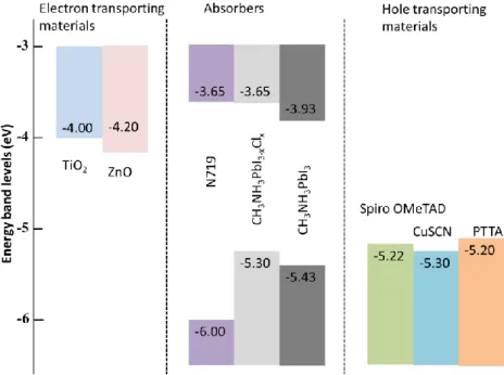
Usually, a p-type conducting organic polymer is used as the hole transporting material for PSCs. The HOMO energy level of HTM must be higher than the valence band of perovskite for the hole transportation. The HOMO energy levels for hole transporting materials tested for PSCs such as spiro-OMeTAD, CuSCN, and PTTA are shown in Figure 1.13; however, spiroOMeTAD, where HOMO energy level is -5.22 eV and the energy level of valence band of (CH3NH3)PbI3 perovskite is -5.43 eV,
is commonly used due to its HOMO fits better with valence band of perovskite.98
Figure 1.13. Energy levels of the typical materials use in solar cells
The HTM layer is coated on the perovskite absorber layer using the spin-coating technique. The thickness of the HTM layer and additives used for the HTM preparation highly effect on the PSCs performances. The charge transport resistance of the HTM layer is quite small for the thickness up to around 140 nm. As the HTM layer thickness is increased above 140 nm, the large increase in the charge transport resistance in HTM layer cause series resistance to arise which leads to a decrease in the FF and thus in the overall cell performances. The additives used in the HTM solution, LiTFSI and TBP, also affect PSCs performances. LiTFSI acts as dopant of the spiro-MeOTAD hole conductor to improve the conductivity. TBP adsorbed on TiO2 surface at pinholes of perovskite layer block the charge recombination at
27
pinholes which increase the electron lifetime, and shift the TiO2 conduction band to
lower energy levels. Devices without any LiTFSI have shown high-transport resistance in the HTM layer. The increase in concentration of TBP results in an increase of the series resistance, leading to lower FF devices. At high-TBP content the increase of the recombination resistance and upward shifting the conduction band cause VOC to enhance.99
A counter electrode, to obtain a circuit in which electrons and holes can transfer through the solar cell, is formed on the HTM layer. As shown in Figure 1.10b, the Fermi levels of the counter electrode must be higher than the HOMO level of HTM. Metallic materials, such as Au, Ag and Al, are used for the counter electrode. These metallic materials are thermally evaporated on the HTM layer.
1.4.5. Equivalent Circuit Model of PSCs
Figure 1.14(a) shows the equivalent circuit model for representing the PSCs, where Rrc and Cµ are resistance associated to the electron-transfer resistance at the
TiO2/perovskite interface and capacitance of the interface; RHTM and CHT M are
resistance and capacitance in the HTM; Rs is attributed to the total series resistance of
wiring, FTO, and blocking layers. In the impeda nce spectrum (Figure1.14(b)), the high frequency arc is due to RHT M and CHTM, the low frequency arc is attributed to Rrc
and Cµ.100 The displacement of the high- frequency arc from the origin is attributed to
the Rs. The RHTM and Rrc resistances of PSCs can be evaluated from the diameter of
the corresponding arcs in the impedance spectrum as shown in Figure 1.14b. The Rs
28
Figure 1.14. Impedance spectroscopic analysis of the perovskite solar cells: (a) equivalent
circuit model; (b) impedance spectrum
A large transport resistance in the HTM, high-RHT M, leads to a low-FF and thus the
overall cell power conversion efficiency. However, this RHT M/CHTM element arc is
disappeared in PSCs with high-conductive HTMs, leaving a single arc in the impedance spectrum.101
Other parameters such as CHTM, Cµ, and τn can be calculated as discussed in
section1.3.6. It has been reported the main difference in the impedance parameter variations of the DSSC and PSC is the behavior of Cµ. With increasing the applied
bias Cµ is increased for the DSSC but, Cµ first decrease and then increase for the PSC;
nonetheless, Cµ of the PSC is lower than that of the DSSC as a result of the different
ionic environment at TiO2.99
1.4.6. Ferroelectricity and Ferroelectric Solar Cells (FESCs)
Ferroelectricity is characterized by a spontaneous polarization which induced by a non-centrosymmetric crystal structure.102Generally, ferroelectric materials undergo a
29
cooling through the Curie temperature, Tc. Above Tc, the crystal has a
centrosymmetric structure and has no spontaneous polarization. Below Tc, the crystal
exhibits ferroelectricity resulting from a change in the symmetry of the unit cell. As a perovskite ferroelectric is cooled below Tc, the central ion in the unit cell displaces
from its equilibrium position to create a spontaneous polarization. For example, barium titanate (BaTiO3) is in a paraelectric phase with no net spontaneous
polarization above Tc (120 °C), but adopts a polar tetragonal phase in the temperature
range 5 to 120 °C. The polar tetragonal phase has six stable polarization directions parallel to the edges of the unit cell.103 Figure 1.15 shows a schematic diagram of the
phase transition and the spontaneous polarization directions in ferroelectric tetragonal phase.
Figure 1.15. Phase transformation from paraelectric cubic phase to ferroelectric tetragonal
phase in BaTiO3; arrows indicate the polarization directions
By applying an electric field, the polar direction of the unit cells can be forced into alignment with the field. This reorientation of spontaneous polarization, known as ferroelectric switching, also induces straining of each unit cell, leading to a macroscopic change in the dimensions and net polarization of the crystal.103 The
polarization switching can be observed by the polarization-electric field (P-E) hysteresis loop, an important characteristic of a ferroelectric. Figure 1.16 shows a typical P-E hysteresis loop. The net polarization of an initially unpolarized ferroelectric material is zero. When an electric field is applied, there is a linear
30
relationship between switchable polarization and the applied electric field for a paraelectric material. In this case, there is no polarization switching. For a ferroelectric material, however, as the applied electric field increases, polarization domains in which the direction of spontaneous polarization is opposite to electric field begin to switch to a more energetically favorable direction. The switching process continues until all of the domains are aligned in the electric field direction. When the field returns to zero, the polarization does not return back to the initial value. The amount of switchable polarization after removal of the applied electric field is called the remnant polarization, Pr. The strength of the applied electric field to switch the
opposite polarization domain is called the coercive electric field, Ec.
Figure 1.16. A typical polarization-electric field (P-E) hysteresis loop. Arrows indicate states
of the material at the corresponding applied electric fields
The ferroelectric materials can be applied to a new type of photovoltaic devices, ferroelectric solar cells (FESCs), which are different from the conventional photovoltaic (PV) devices, whose charge separations are heavily determined by the intrinsic built- in electric field generated by the spontaneous polarization; thus, ferroelectric polarization plays a dominant role in charge separation and transport.104,105 FESC can generate above bandgap open circuit voltages and also
31
switching.104 Ferroelectric solar cells based on several inorganic ferroelectric oxide
thin films have been studied, including BiFeO3,106 and Pb(Zr,Ti)O3.107
The outstanding photovoltaic performance of PSCs may be attributed to the ferroelectric nature of the perovskite materials.108-113 Hence, in-depth systematic
studies on the structural and ferroelectrics of the perovskites absorbers and its impact on the charge transfer mechanism in PSCs is imperative for future developments.
1.5.Purpose of Present Study
Dye-sensitized solar cells (DSSCs) and perovskite solar cells (PSCs) have attracted great interest of the researchers due to their low-cost potentials on converting solar power to electrical power. However, DSSCs suffer from low efficiencies and lots of studies have been reported on dye molecular engineering and electrochemical engineering of TiO2 nanoparticles for photoelectrodes with limited studies on
interface engineering. On the other hand, PSCs as a novel generation of solar cells have competitive efficiencies to market available Si-solar cells, but its mysterious working mechanism severely hampers further improvements of the materials and device structures for the future developments.
Objectives of the present study;
To enhance dye-sensitized solar cells performances by engineering the interface between nanocrystalline TiO2 electrode and electrolyte solution using
dye and silane adsorptions.
To improve dispersion ability of TiO2 nanoparticles in their pastes by
modification of TiO2 nanoparticle surface with organic molecules to minimize
TiO2 surface energy.
To clarify the working mechanism of the PSCs based on the ferroelectric behavior.
Following chapters describe how the above objectives are achieved. Chapters II, and III present the interface engineering between the nanocrysta lline TiO2 electrode