INVITED PAPER
Special Section on Electronic DisplaysE
ffects of Additive Elements on TFT Characteristics in Amorphous
IGZO Films under Light Illumination Stress
Shinya MORITA†a), Satoshi YASUNO†, Aya MIKI†, and Toshihiro KUGIMIYA†, Nonmembers
SUMMARY We have studied effects of additive elements into the chan-nel layers of amorphous IGZO TFTs on threshold voltage shift issues un-der light illumination stress condition. By addition of Hf or Si element, the Vthshift under light illumination and negative bias-temperature stress and illumination stress conditions was drastically suppressed while the switch-ing operation of TFTs usswitch-ing IGZO with Mn or Cu was not observed. It was found that the addition of Si or Hf element into the IGZO channel layer leads to reducing the hole trap sites formed at or near the gate insula-tor/IGZO channel interface.
key words: thin-film-transistor, oxide semiconductor trap density, stability 1. Introduction
Amorphous oxide semiconductors (AOSs) such as a-IGZO [1]–[3], a-IZO [4] and a-ZTO [5] are promising materi-als for thin film transistors (TFTs) in flat-panel displays (FPDs) because AOS films have larger channel mobility above 10 cm2/Vs, a simpler deposition process, and a better uniformity over large area in comparison with conventional amorphous and polycrystalline Si films. For practical appli-cations, however, the reliability and the stability issues of AOS-TFTs, such as the threshold-voltage (Vth) shifts which
are occasionally observed under various stress condition during the TFT operation [6], [7], need to be further solved. In particular, the stability under the light-illumination and negative bias-temperature stress (LNBTS) is one of the crit-ical issues because the negative bias is mostly applied to AOS TFTs that are always illuminated by the leaked back light of LCD display [8].
Generally, Vthshifts are caused by the accumulation of
carriers in a bulk and/or at the interface between the AOS and the adjacent gate insulator layers under the stresses [9]. In the case of LNBTS, it is proposed that the reason of the instability is due to holes which are excited by the light illu-mination and trapped at the interface between the AOS and the gate insulator layers [10]. On the other hand, it is known that there are deep defect states called sub-gap states near the valence band maximum (VBM) [11]. These sub-gap states might be the origin site of hole capture under LNBTS condition.
Several researchers have attempted to improve TFT stability under various stress conditions by optimization of the AOS film deposition and TFT fabrication conditions.
Manuscript received March 2, 2011. Manuscript revised June 7, 2011.
†The authors are with KOBE STEEL, LTD., Kobe-shi, 651-2271 Japan.
a) E-mail: [email protected] DOI: 10.1587/transele.E94.C.1739
For example, annealing in H2O vapor improves AOS-TFT
characteristics due to the suppression of shallow tail states near conduction band [12]. Furthermore, it is reported that the material selection and the deposition process optimiza-tion of gate insulator and passivaoptimiza-tion layers are effective to suppress the Vth shift under various bias stresses [6], [7],
[13], [14].
In this study, we have investigated the effects of addi-tive elements into a-IGZO channel layers on Vthshift issue
under LNBTS condition in TFTs. It is expected that the ad-dition of elements results in the improvement of electronic structure of the bulk and the gate interface region of IGZO channel layers on the Vthshift issue.
2. Experimental
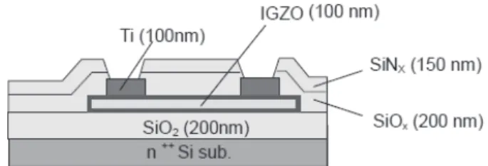
In the present study, a-IGZO TFTs with a bottom gate struc-ture were fabricated to investigate the effect of additive X element, which contained either Cu, Hf, Mn or Si into IGZO channel layer (i.e. IGZO+X), on TFT characteristics. Fig-ure 1 schematically shows the cross sectional view of a-IGZO TFT. The TFTs were fabricated on n-type Si sub-strates covered with a 200-nm thick, thermally grown SiO2
layer as a gate insulator. The IGZO or IGZO+X (X = Cu, Hf, Mn, or Si) channel layer (thickness: 100 nm) were de-posited on SiO2by RF magnetron sputtering using each
sin-gle sputtering target. In some experiments, double-layered channel with IGZO+Si (5 nm) as the bottom layer and IGZO (95 nm) as the top layer on SiO2 gate insulator were
de-posited to clarify the effect of additive element at whole channel layer (bulk) or gate interface. After the patterning of the IGZO channel layer, the specimens were annealed at 350◦C for 1 h in O2 atmosphere. The source/drain
elec-trodes (Ti) with a 100-nm thickness were then deposited by DC sputtering, and patterned by lift-off process. Finally, a stacked layer of SiNx (top)/SiOx (bottom) was deposited
by PE-CVD at 150◦C as a passivation layer. The channel
Fig. 1 Schematic of bottom gate TFT structure (L/W) = 10/200 µm.
length (L) of TFT was 10 µm and the channel width (W) was 200 µm. The TFT characteristics were measured us-ing a semiconductor parameter analyzer (Keithley 4200) un-der dark and illuminated conditions. The drain voltage was fixed at 10 V during the measurements.
First, we investigate Id− Vgcharacteristics of IGZO+X
(X = Cu, Hf, Mn, or Si) TFTs at room temperature un-der dark condition, and field effect mobility (µFE), threshold
voltage (Vth) and sub-threshold swing (SS) are calculated by
their Id− Vg characteristics. Then, the Id − Vg
characteris-tics of IGZO, IGZO+Si, and IGZO+Hf TFTs under LNBTS condition were also measured. In the LNBTS test, the illu-minated condition with a wavelength of 400 nm and maxi-mum power density 0.1 µW/cm2was set, while the negative
bias stress was fixed at−20 V (Vd= 10 V). The temperature
applied for thermal stress was 60◦C and these condition was kept up to 3600 s. The Id−Vgcharacteristics were measured
at 10, 100, 1000, and 3600 s.
In addition, the Id − Vg characteristics of IGZO
and IGZO+Si TFTs under light illumination and high-temperature conditions (LT) were measured to clarify the difference from the Id − Vg under LNBTS condition. The
same wavelength as LNBTS and the power density of 6.6 µW/cm2 were used. For LT test, the I
d − Vg
charac-teristics of IGZO and IGZO+Si TFTs were evaluated and compared in dark and LT conditions. The Id− Vghysteresis
from Vg = −30 V to 30 V (forward sweep) and Vg = 30 V
to−30 V (reverse sweep) were measured under both dark and LT conditions at 60◦C that is the same temperature for LNBTS. The drain voltage was also fixed at 10 V.
3. Results and Discussion
3.1 TFT Characteristics of IGZO+X
Figure 2 shows Id − Vg characteristics of IGZO (as
refer-Fig. 2 Id− Vgcharacteristics of IGZO+additive element X, (a) reference IGZO, (b) 2.3 at.%Hf, (c) 2.4 at.%Si, (d) 0.6 at%Cu, and (e) 0.7 at.%Mn.
ence), IGZO+ 2.3 at.% Hf, IGZO+2.4 at.%Si, IGZO+0.6 at.%Cu, and IGZO+0.7 at.%Mn TFTs, respectively, mea-sured under dark at room temperature condition. The pa-rameters, Vth, SS and µFE in each TFT evaluated from
Id− Vg characteristics, are summarized in Table 1. While
the Vth, SS, µFE were−1.4 V, 0.47 V/decade, 14.2 cm2/Vs,
respectively, in the case of the reference IGZO TFT, both IGZO+Hf and IGZO+Si TFTs showed similar characteris-tics although µFEfor IGZO+Hf and IGZO+Si were slightly
lower than that of reference IGZO TFT. On the other hand, in the IGZO+Mn and IGZO+Cu TFTs, Id− Vg
characteris-tics could not show the switching operation. Figure 3 shows the dependence of µFEon Hf or Si content into IGZO
chan-nel layer in the TFT. It is seen that the values of µFE
de-creased with increasing the amount of additive elements (Hf or Si) into the channel layer. It considers that Hf or Si el-ement addition into IGZO channel layer are detrimental to the electron mobility as electrons are scattered by Hf or Si element. Therefore, addition amount of Hf or Si element should be limited to be below a few atomic percent not to reduce the µFE in the TFTs. On the other hand, the TFT
containing 1 at.% Mn or Cu did not show the switching op-eration. In the case of Cu and Mn addition, the resistivity of the films drastically increased. It is speculated that the donar was compensated by the gap states, probably accepter-like, formed by Cu or Mn incorporated in the film.
3.2 Light and Negative Bias Stress of IGZO TFTs We also investigated the stability of reference IGZO,
Table 1 SS, Vthand mobility of IGZO+X TFTs.
Fig. 4 Id− Vgcharacteristic of (a) IGZO and (b) IGZO+2.4 at.%Si TFT
under LNBTS condition.
IGZO+2.3 at.%Hf, IGZO+2.4 at.%Si TFTs under LNBTS condition. Figures 4(a) and (b) show Id − Vg
characteris-tics of IGZO and IGZO+Si TFTs under LNBTS condition. As shown in this Figure, IGZO and IGZO+Si TFTs ex-hibited a negative Vth shift. The Vth shift values in IGZO
and IGZO+Si TFTs were −6.2 V, and −1.5 V for 3600 s, re-spectively. It was thus clearly demonstrated that the Si el-ement addition could suppress the Vth shift under LNBTS
condition. Figure 5 shows the time dependence of the Vth
shift (ΔVth) from the 0 (first sweep) to 3600 s in IGZO,
IGZO+Hf, and IGZO+Si. The ΔVth was as low as 0.6 V
in IGZO+Hf, and ΔVth was saturated at 3600 s, as well as
the stability of Vth under LNBTS condition was improved
by Hf or Si element addition into IGZO channel layer. As described above, additive elements of Hf or Si sup-pressed the Vthshift under LNBTS condition. It considers
that these elements have the effect of reduction of hole trap sites considering the Vthshift under LNBTS condition was
reported to be due to the holes trapped at the interface be-tween the gate insulator and the channel layer [10].
Fig. 5 ΔVthof IGZO, IGZO+Hf and IGZO+Si channel in TFTs uner LNBTS condition.
Fig. 6 Id− Vgcharacteristics of IGZO TFT in dark and LT conditions.
3.3 TFT Characteristics of IGZO under the Light Illumi-nation
In order to investigate the effect of reduction of hole trap sites in IGZO+Si TFT, we measured Id− Vgcharacteristics
in LT condition. Especially, in LT condition, we used the higher illumination power density than that in LNBTS con-dition to evaluate the hole trap phenomena during one Vg
sweep. Figures 6 and 7 show the Id− Vgcharacteristics in
IGZO and IGZO+Si TFTs under dark and LT conditions. In the dark condition, the difference of Vth in forward and
re-verse sweeps is 1.0 V. In the LT condition, the difference of Vthincreased to 3.8 V because the change of Id− Vg
charac-teristics was seen during forward Vgsweep.
The changes of Vthand SS in appearance under LT
con-dition during forward Vg sweep could be explained that it
is due to the holes which are excited by light illumination and trapped at the interface between the gate insulator and the channel layers [15], as shown in Fig. 8(a). Electron-hole pairs are continuously excited by the light illumination with the energy more than the band gap of IGZO (around 3.2 eV). In the beginning of the forward Vg sweep, higher negative
Fig. 7 Id− Vgcharacteristics of IGZO+Si TFT in dark and LT conditions.
Fig. 8 Band diagram of IGZO TFT under LT condition.
This leads to the trap of the holes at the interface, as well as electrons are swept along the electrical field. On the other hand, in the case of reverse Vgsweep, Vthshift could not
oc-cur because the holes trapped at the interface during forward
Vg sweep were swept due to the higher positive Vg bias as
shown in Fig. 8(b). Therefore, neither Vthnor the
degrada-tion of SS occurs in reverse Vgsweep.
Thus, in the Id−Vgcharacteristics of IGZO+Si TFT
un-der LNBTS and LT conditions as shown in Figs. 4(b) and 7, it was found that Si element addition into IGZO channel layer is really effective to reduce the hole trap sites at the interface between gate insulator and channel layers. On the other hand, as shown in Fig. 3, adding Si element into IGZO channel layer itself leads to reduction of µFE. As the results,
the effect of the reduction of hole trap sites might be larger than the reduction of µFEif the amount of Si addition is
lim-ited to be below a few atomic percent. Actually, we investi-gated the band tail states (i.e. Urbach tail energy estimated from optical absorption spectra) of IGZO and IGZO+Si lay-ers. The optical bandgap and Urbach energy in IGZO and IGZO+Si layer were 3.22 eV, 3.25 eV, and 0.15 eV, 0.16 eV, respectively. It was found that the tail energy state (Urbach energy) of IGZO+Si layer is slightly increasing compared with IGZO layer.
Fig. 9 Id−Vgcharacteristics of double-layered channel (IGZO/IGZO+Si) under LNBTS condition.
Fig. 10 The peak position of (a) In3d (b) O1s (c) Zn2p (d) Ga2p in XPS results of a-IGZO and a-IGZO+Si layers after annealing at 350◦C.
3.4 Double-Layered Channel of IGZO and IGZO+Si Films
As mentioned above, Si element addition into IGZO chan-nel layer reduces the hole trap sites at the gate insulator in-terface while the µFEis decreased. In order to confirm these
models, we used the double-layered channel consisting of IGZO (top)/IGZO+Si (bottom) in TFT. Figure 9 shows the
Id− Vg characteristics of double-layered channel of IGZO
(95 nm)/IGZO+Si (5 nm) in TFT under LNBTS condition. The mobility, Vth and SS of the TFT were 13.8 cm2/Vs,
3.0 V, and 0.51 V/decade, respectively. In the LNBTS stress measurement as shown in Fig. 10, the Vthshift (−1.0 V)
ob-served in LNBTS condition is also small compared with IGZO+Si single layer (see Fig. 5). It is considered that Si element addition into IGZO channel has mainly the effect of the reduction of the hole trap sites at the interface of gate in-sulator and channel layers rather than bulk in IGZO channel. Furthermore, the µFEis almost same as that of single-layered
IGZO as shown in Table 1. Finally, by using double-layered structure consisting of IGZO/IGZO+Si films, we found that both the suppression of Vthshift and keeping high µFEcould
be achieved. 3.5 XPS Spectra
It is well known that these instabilities are related to oxygen vacancy in IGZO film and at the interface between gate in-sulator and channel layers, and that high density deep states have been reported by several researches [11], [16]. It is expected that Si doped into IGZO channel layer forms Si-O bond in its IGZO layer. Therefore, IGZO+Si layer might af-fect to reduce the deaf-fects caused by oxygen vacancy because binding energy of Si-O is higher than that of In-O, Zn-O, or Ga-O. Hf-O bond is also high as well as Si-O, Hf ele-ment addition into IGZO channel has the same effect com-pared with Si under LNBTS condition as shown in Fig. 5. Here, the binding energies of IGZO and IGZO+Si layers were analyzed by X-ray Photoelectron Spectroscopy (XPS). Figures 10(a), (b), (c), and (d) show photoelectron peaks of In 3d, O 1s, Zn 2p and Ga 2p in IGZO and IGZO+2.4 at.%Si layers after 350◦C annealing, respectively. In 3d, Zn 2p and Ga 2p peaks hardly changed between IGZO and IGZO+Si layers. On the other hand, the peak position of O 1 s was moved slightly from 530.2 eV to 530.3 eV. It was clear that the binding energy of O 1 s is shifted to higher binding en-ergy by Si addition. This indicates that slight peak shift was caused by an increase of Si-O bond with higher binding en-ergy. As Si element addition into IGZO channel layer is really effective to reduce the hole trap sites at the interface between gate insulator and channel layers, it is thought that strong Si-O bonds might reduce the carrier trap sites (de-fects) at gate insulator interface region including interface and adjacent interface of IGZO+Si layer.
4. Conclusion
We have investigated the effects of additive elements, Hf, Si, Cu, and Mn, into IGZO channel layer on TFT characteris-tics. IGZO+Hf and IGZO+Si TFTs showed a good Id− Vg
characteristics while the values of µFEremained more than
10 cm2/Vs for IGZO+Hf and the IGZO+Si TFTs,
compara-ble to that of the IGZO TFT.
We also investigated the stability of Id−Vg
characteris-tics under dark, LT and LNBTS conditions. It was found that the addition of Hf or Si element into IGZO channel layer suppresses to change Vth under LT and LNBTS
con-ditions. This indicates that the Si or Hf addition can reduce the hole trap sites at interface between the gate insulator and the channel layers.
References
[1] K. Nomura, H. Ohta, A. Takagi, T. Kamiya, M. Hirao, and H. Hosono, “Room-temperature fabrication of transparent flexible thin-film transistors using amorphous oxide semiconductors,” Nature, vol.432, pp.488–492, 2004.
[2] D.P. Gosain and T. Tanaka, “Instability of amorphous indium gal-lium zinc oxide thin film transistors under light illumination,” Jpn. J. Appl. Phys., vol.48, 03B018, 2009.
[3] K. Takechi, M. Nakata, T. Eguchi, H. Yamaguchi, and S. Kaneko, “Temperature-dependent transfer characteristics of amor-phous InGaZnO4thin-film transistors,” Jpn. J. Appl. Phys., vol.48, 011301, 2009.
[4] J.I. Song, J.S. Park, H. Kim, Y.W. Heo, J.H. Lee, J.J. Kim, G.M. Kim, and B.D. Choi, “Transparent amorphous indium zinc oxide thin-film transistors fabricated at room temperature,” Appl. Phys. Lett., vol.90, 022106, 2007.
[5] P. Gorrn, P. Holzer, T. Riedl, and W. Kowalsky, “Stability of trans-parent zin tin oxide transistors under bias stress,” Appl, Phys. Lett., vol.90, 063502, 2007.
[6] J.K. Jeong, H.W. Yang, J.H. Jeong, Y.-G. Mo, and H.D. Kim, “Ori-gin of threshold voltage instability in indium-gallium-zinc oxide thin film transistors,” Appl. Phys. Lett., vol.93, 123508, 2008. [7] K.H. Ji, J.-I. Kim, Y.-G. Mo, J.H. Jeong, S. Yang, C.-S. Hwang,
S.-H.K. Park, M.-K. Ryu, S.-Y. Lee, and J.K. Jeong, “Comparative study on light-induced bias stress of IGZO transistors with SiNx and SiOx gate dielectrics,” IEEE Electron. Device. Lett., vol.31, pp.1404–1406, 2010.
[8] K.H. Lee, J.S. Jung, K.S. Son, J.S. Park, T.S. Kim, R. Choi, J.K. Jeong, J.-Y. Kwon, B. Koo, and S. Lee, Appl. Phys. Lett., vol.95, 232106, 2009.
[9] J. Lee, J.-S. Park, Y.S. Pyo, D.B. Lee, E.H. Kim, D. Stryakhilev, T.W. Kim, D.U. Jin, and Y.-G. Mo, “The influence of the gate dielectrics on threshold voltage instability in amorphous indium-gallium-zinc oxide thin film transistors,” Appl. Phys. Lett., vol.95, 123502, 2009.
[10] K.-H. Lee, J.S. Jung, K.S. Son, J.S. Park, T.S. Kim, R. Choi, J.K. Jeong, J.-Y. Kwon, B. Koo, and S. Lee, “The effect of moisture on the photon-enhanced negative bias thermal instability in Ga-In-Zn-O thin film transistors,” Appl. Phys. Lett., vol.95, 232106, 2009. [11] K. Nomura, T. Kamiya, H. Yanagi, E. Inagawa, K. Yang, K.
Kobayashi, M. Hirano, and H. Hosono, “Subgap states in trans-parent amorphous oxide semiconductor, In-Ga-Zn-O, observed by bulk sensitive x-ray photoelectron spectroscopy,” Appl. Phys. Lett., vol.92, 202117, 2008.
[12] K. Nomura, T. Kamiya, M. Hirano, and H. Hosono, “Origins of threshold voltage shifts in room-temperature depsited and an-nealed a-In-Ga-Zn-O thin-film transistors,” Appl. Phys. Lett., vol.95, 013502, 2009.
[13] H.-H. Hsieh, J.-Y. Huang, W.-P. Huang, Y.-H. Lin, and C-C. Wu, “IGZO TFTs with good environmental stability and short-range uni-formity,” Proc. IDW’09, pp.1681–1684, 2009.
[14] J.K. Jeong, J.H. Jeong, J.H. Choi, J.S. Im, S.H. Kim, H.W. Yang, K.N. Kang, K.S. Kim, T.K. Ahn, H.-J. Chung, M. Kim, B.S. Gu, J.-S. Park, Y.-G. Mo, H.D. Kim, and H.K. Chung, “12.1-Inch WXGA AMOLED display driven by indium-gallium-zinc oxide TFTs ar-ray,” Proc. SID 08 DIGEST, vol.39, pp.1–4, 2008.
[15] S.Y. Lee, S.J. Kim, Y.W. Lee, W.G. Lee, K.S. Yoon, and M.K. Han, “Light induced hysteresis phenomenon in amorphous oxide-based thin film transistors,” Proc. AM-FPD’10, p.137, 2010.
[16] H. Oh, S.-M. Yoon, M.K. Ryu, C.-S. Hwang, S. Yang, and S.-H.K. Park, “Photon-accelerated negative bias instability involving subgap states creation in amorphous In-Ga-Zn-O thin film transistor,” Appl. Phys. Lett., vol.97, 183502, 2010.
Shinya Morita received the B.Sci. and M.Sci. degrees in physics from Hiroshima Uni-versity in 2005 and 2007 respectively. Since he joined Kobe Steel, LTD., Kobe, Japan in 2007, he has extensively explored new metal film ma-terials for interconnection of FPD. He has in-volved himself in the studies on development new oxide materials and fabrication processes of oxide TFTs for FPD. He received the Outstand-ing Poster Paper Award of IDW in 2010 for re-search of new oxide semiconductor materials.
Satoshi Yasuno received the B.Eng. and M.Eng. degrees in applied chemistry from Gifu University in 2001 and 2003 respectively. In 2003, he joined Kobelco Research Insti-tute, Inc., Kobe, Japan in 2003, and has been working on physical analysis particularly with high-resolution Rutherford back scattering spec-troscopy. Since 2009 he joined a project for OX-IDE semiconductor for FPD in Electronics Re-search Lab. in KOBE STEEL, he has character-ized physical property of OXIDE semiconductor and developed evaluation method for film quality of OXIDE semiconductor with Microwave photoconductivity decay. Currently at Kobelco Research Institute, Inc.
Aya Miki received the B.Sci. and M.Sci. de-grees in physics from Tohoku University in 2003 and 2005, respectively. Since she joined Kobe Steel, LTD., Kobe, Japan in 2005, she has ex-tensively explored new alloy films for intercon-nection for FPD. Since 2009 when she joined a project for oxide TFTs for FPD, she has ex-plored characteristics of oxide TFTs.
Toshihiro Kugimiya received the B.Eng., M.Eng. and Dr. degrees in electronics engineer-ing from Toyohashi University of Technology in 1991, 1993, and 2011, respectively. In 1993, he joined KOBE STEEL, LTD., Japan, and he has worked on metal interconnections for FPD, es-pecially, Al-alloy film interconnections. Since 2009 when he joined a project for OXIDE semi-conductor for FPD in Electronics Research Lab. in KOBE STEEL, he has directed the researches of OXIDE-TFT fabrication process and analyses of OXIDE materials and TFTs.