194
IEICE TRANS. ELECTRON., VOL.E92–C, NO.2 FEBRUARY 2009
INVITED PAPER
Special Section on Recent Advances in Integrated Photonic DevicesHigh-Power Pure Blue InGaN Laser Diodes
Atsuo MICHIUE†a), Takashi MIYOSHI†, Tokuya KOZAKI†, Tomoya YANAMOTO†, Shin-ichi NAGAHAMA†, and Takashi MUKAI†, Nonmembers
SUMMARY We fabricated high-power pure blue laser diodes (LDs) by using GaN-based material for full-color laser display. The operating output power, voltage and wall-plug efficiency of the LDs at forward current of 1.0 A were 1.17 W, 4.81 V and 24.3%, respectively. The estimated lifetime of the LDs was over 30,000 hours under continuous-wave operation.
key words: InGaN, GaN, high-power laser, blue LD
1. Introduction
In late years, laser light has drawn attention as light source for full color display. Using the lasers with three primary colors leads to the wider color coordination compared with the conventional display one. The red and green laser light sources have been developed by AlInGaP material and sec-ond harmonic generation (SHG) laser, respectively. For the blue laser light source, we have reported the blue LDs at 445 nm with output power at 500 mW [1]. However, upsiz-ing the recent display requires the higher output power in lasers light source. For this objective, we succeeded in de-veloping the high-power (1 W) and high-efficiency pure blue laser diodes (LDs). We reported the corresponding charac-teristic of the high power pure blue LD in this work.
2. Experiment
The schematic picture of the high-power blue LDs is shown in Fig. 1. The LD was grown on c-plane freestanding GaN substrates [2] by the metal organic chemical vapor deposi-tion (MOCVD). The LD structure was based on separate confinement heterostructure multiple quantum well (SCH-MQW) with ridge-waveguide [1]. The cavity facet was formed by cleavage an m-plane facet.
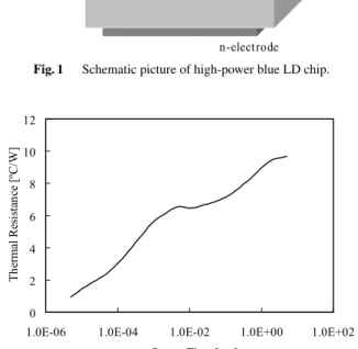
We employed a new package in order to lower the ther-mal resistance for the realization of higher output power. The diameter of a new package wasφ9 mm. The laser chip was mounted in a p-side up configuration. The thermal re-sistance of the new package is shown in Fig. 2. The thermal resistance at 1.0 A forward current under continuous-wave (cw) operation at 25◦C was 10◦C/W.
Manuscript received June 25, 2008. Manuscript revised October 28, 2008.
†The authors are with LD Development Department, LD
En-gineer Division, Optelectronics Products Business Unit, Nichia Corp., Tokushima-shi, 774-8601 Japan.
a) E-mail: [email protected] DOI: 10.1587/transele.E92.C.194
Fig. 1 Schematic picture of high-power blue LD chip.
Fig. 2 Thermal resistance of high-power blue LD withφ9 mm package.
3. Characteristics of Blue LDs
The typical current-voltage (I-V) and current-output power (I-L) characteristics of the high power blue LDs under cw operation at 25◦C are shown in Fig. 3. The threshold cur-rent was 184 mA, and the operating output power, voltage and wall-plug efficiency at forward current of 1.0 A were 1.17 W, 4.81 V and 24.3%, respectively. Wall-plug effi-ciency reaches up to 24% at 1.2 A forward current.
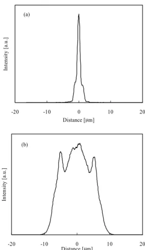
Figure 4 shows the typical far field patter (FFP) at 1.0 A forward current under cw operation at 25◦C. Beam diver-gence angle in fast, and slow axis at the intensity of 1/e2
indicated 38.2◦ and 11.7◦, respectively. FFP in fast axis is nearly Gaussian distribution. On the other hand, we ob-served the mixed shape with multi peaks at FFP in a slow axis due to the transverse mode being multi mode.
MICHIUE et al.: HIGH-POWER PURE BLUE INGAN LASER DIODES
195
Fig. 3 Typical L-I and V-I characteristics of blue LDs under cw operation at 25◦C.
Fig. 4 Typical far field pattern in (a) fast axis and (b) slow axis of high-power blue LDs at current of 1.0 A under cw operation at 25◦C.
The typical near field pattern (NFP) at forward current of 1.0 A under cw operation at 25◦C is shown in Fig. 5. The emitting size in slow axis was 16μm × 1 μm which is almost the same ridge-width.
The typical emission spectrum at 1.0 A forward current under cw operation at 25◦C is shown in Fig. 6. The multi-mode emission was observed at around 445 nm.
The L-I characteristics in the pulsed condition (duty 1%, Cycle 200μsec) at 25◦C is shown in Fig. 7. The output power in the pulsed condition of the LDs was over 3 W and
Fig. 5 Typical near field pattern in (a) fast axis and (b) slow axis of high-power blue LDs at current of 1.0 A under cw operation at 25◦C.
Fig. 6 Typical emission spectrum of high-power blue LDs at forward current of 1.0 A under cw operation at 25◦C.
the catastrophic optical damage (COD) was unconfirmed at the facet of the cavity. The optical power density at the out-put power of 3.0 W was about 19 MW/cm2.
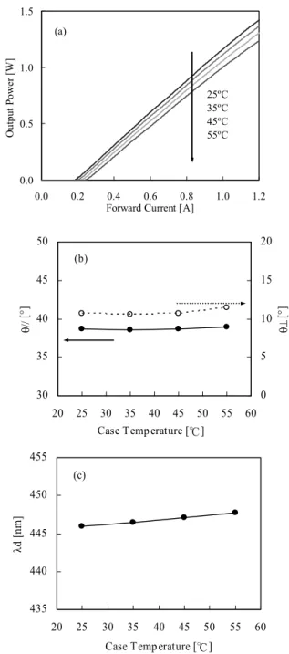
The temperature dependences of L-I characteristics, FFP and dominant wavelength are shown in Figs. 8(a), (b) and (c), respectively. From Fig. 8(a), the threshold current increased with increasing the temperature, and characteristic temperature (T0) was 105 K. However, the deterioration of
196
IEICE TRANS. ELECTRON., VOL.E92–C, NO.2 FEBRUARY 2009
Fig. 7 Typical L-I of high-power blue LDs under pulsed operation at 25◦C.
the slope efficiency was unobservable by increasing a tem-perature. The FFP width in both slow and fast axis was un-changed by varying the shown in Fig. (b). The red sift of emission wavelength was 0.06 nm./◦C in Fig. (c).
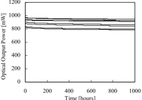
A lifetime test of high-power blue LDs was carried out at a temperature of 25◦C under 1.0 A automatic current con-trol (ACC) condition. The result of the lifetime tests is shown in Fig. 9. The lifetime was defined as the expected time when the output power of the LDs reached 50 percent from the initial output power. The lifetime was estimated to be over 30,000 hours at 1000 hours operation. As a result, we confirmed the long-term reliability of the high-power blue LDs.
4. Conclusion
We succeed in fabricating high-power blue LDs with an op-tical output power of 1 W by using GaN-based material. The operating output power, voltage and wall-plug efficiency of the LDs at forward current of 1.0 A were 1.17 W, 4.81 V and 24.3%, respectively. The output power in the pulsed condi-tion of the LDs was over 3 W. The estimated lifetime of the LDs was over 30,000 hours under cw operation.
References
[1] T. Miyoshi, T. Kozaki, T. Yanamoto, Y. Fujimura, S. Nagahama, and T. Mukai, “GaN-based high power blue laser diodes for display appli-cations,” SID2006 Digest, pp.1915–1917, 2006.
[2] K. Motoki, T. Okahisa, N. Matsumoto, M. Matsushima, H. Kimura, H. Kasai, K. Takemoto, K. Uematsu, T. Hirano, M. Nakayama, S. Nakahata, M. Ueno, D. Hara, Y. Kumagai, A. Koukitu, and H. Seki, “Preparation of larg freestanding GaN substrates by hydride vapor phase epitaxy using GaAs as a starting substrate,” Jpn. J. Appl. Phys., vol.40, pp.L140–L143, 2001.
Fig. 8 Temperature dependences of (a) L-I characteristics, (b) FFP-width of intensity of 1/e2 and (c) dominant wavelength of high-power blue LDs at forward current of 1.0 A under cw operation at 25◦C.
MICHIUE et al.: HIGH-POWER PURE BLUE INGAN LASER DIODES
197
Fig. 9 Result of lifetime test under ACC with forward current of 1.0 A under cw operation at 25◦C.
Atsuo Michiue received the B.S. de-gree in chemical engineering form Doshisha in 1999 and M.S. degree in chemical engineering from Nara Institute of Science and Technology (NAIST) in 2000 and 2001, respectively. He is now with NICHIA Corporation.
Takashi Miyoshi received the M.S. degree in engineering from Osaka City University in 2000. He has joined NICHIA Corporation and developed the GaN semiconductor laser in the Development Division of NICHIA Corporation from 2000.
Tokuya Kozaki received the M.S. degree in engineering from Tokushima University in 1995. He has joined NICHIA Corporation and developed the GaN semiconductor laser in the Development Division of NICHIA Corporation from 1995.
Tomoya Yanamoto received the M.S. de-gree in engineering from Tokyo University of Science in 1996. He has joined NICHIA Cor-poration and developed the GaN semiconductor laser in the Development Division of NICHIA Corporation from 1996.
Shin-ichi Nagahama received the B.S. in the electronic engineering from Tokushima Uni-versity in 1991. He received the Ph.D. degree in engineering from Tokushima University in 2002. He has joined Nichia Corporation and de-veloped GaN semiconductor laser.
Takashi Mukai received the B.S. degree in the in the electronic engineering from Toku-shima University in 1987. He received Ph.D. degree in engineering from Tokushima Univer-sity in 2000. He has joined NICHIA Corpora-tion and developed the light emitting device of GaAs, GaN semiconductor lin the Development Division of NICHIA Corporation from 1987. He is a General Manager in Nitride Semicon-ductor Research Laboratory.