Study on the Characteristics of Electrochemically Prepared Copper Oxide Photovoltaic Devices
( 電気化学的に形成した酸化銅光電変換素子の特性に関する研究 )
January, 2019
Doctor of Philosophy (Engineering)
Pei Loon Khoo
Toyohashi University of Technology
別紙4-1(課程博士(英文))
Date of Submission(month day,year): January 07, 2019
Department
Mechanical Engineering Student ID Number
D 145108
Supervisors
Masanobu Izaki
Applicant’s name
Pei Loon Khoo Seiji Yokoyama
Abstract(Doctor)
Title of Thesis
Study on the Characteristics of Electrochemically Prepared Copper Oxide
Photovoltaic Devices
(電気化学的に形成した酸化銅光電変換素子の特性に関する研究)
Approx. 800 words
Solar cells, or photovoltaics (PV), which converts light into electricity using semiconductor materials, are proving to be essential and indispensable for a sustainable society. Numerous kinds of solar cells have been the focus of research interest of late, and thin solid films of metal oxide (MO) semiconductors, such as copper oxide based photovoltaics (PV) has always been considered a material suitable for the realization of low-cost solar cells. Cuprous Oxide (Cu
2O) and Cupric Oxide (CuO) are stable forms of copper oxides, at the same time being intrinsically p-type semiconductors with 2.1 eV and 1.4 eV respectively. Attractive points of these oxides originate from their non-toxicity, abundance, and low cost. Also, one main aspect of interest to be noted is the preparation process, which can be achieved by electrochemical preparation.
Electrochemically-prepared ZnO/Cu
2O PV had been reported to achieve 1.28%, however, the theoretical limit is approximately 20% according to the Shockley-Queisser Efficiency Limit, based on the bandgap energy. The main objective of this research is to further investigate the limiting factors of copper oxide based electrochemically-prepared photovoltaics and methods to further increase the PCE, based on close studies on the properties of its solid state physics.
In this thesis, in Chapter 1, the introduction, background, review, and purpose of this study are discussed. Latest climate researches are briefly concluded and the urgency of addressing global warming by switching to renewable energy, and the importance of solar energy is discussed. Metal Oxide (MO) PVs has the criteria of a high-potential candidate as cheap, and widespread. Among these MOs, Copper Oxides possess unique preferable properties such as ideal bandgap energies, at the same time being able to be fabricated by simple methods like the electrochemical preparation. It is then necessary to investigate the electrochemically- prepared copper oxides from its solid state physics. The definition of power conversion efficiency (PCE) is proportional to the short-circuit current density (J
SC) and open-circuit voltage (V
OC) of a PV. However, the independent variables of preparations are wide and complex, and insufficient information calls for the detailed study of determining the affecting factor during preparations. Also, a strategy using multiple bandgaps (using both copper oxide) as the light-absorbing layer is discussed.
In Chapter 2, we report the fabrication of basic Cu
2O-only (GZO/ZnO/Cu
2O) PV, and the
successful increase in J
SCalong with external quantum efficiency (EQE) and carrier mobility
(µ), by annealing in vacuum using a rapid thermal annealer (RTA). The optimum annealing
temperature was found to be 423 K. The effect of annealing during preparation is further
studied in detail, which includes its microstructural, optical and electrical properties. The mechanism is discussed, and the elucidation of the mechanism concludes a contributing factor of increased carrier mobility due to decreased scattering defects. Also, the relationship between the interface structure and V
OCis discussed.
In Chapter 3, we report the photovoltaic properties of CuO-only (CuO/Polysiloxane/GZO) successfully fabricated by electrodeposition from a basic aqueous solution containing copper acetate hydrate and ammonia with highly resistive polysiloxane layer insertion as the buffer layer. This study indicates the ability of CuO to function as a PV, which validates the strategy of using both Cu
2O and CuO as the light absorbing layer to increase the light-absorption width.
In Chapter 4, we report the fabrication of directly stacked (GZO/Cu
2O/CuO) photoactive layer prepared by electrodeposition and annealing. A decrease in EQE due to the formation of nanopores and voids was observed. However, the EQE was studied in detail and showed an expansion of absorption width which originates from the charge collection of both the Cu
2O and CuO layer, with a two-way carrier transport. When a low reverse biased voltage was applied, the charge collection corresponding to the absorption edge originating from the CuO layer could be clearly observed due to improved carrier control. However, there is a necessity for an in-depth investigation into the energy states and the band alignment of the Cu-oxide PV.
Chapter 5 reports on the study of chemical and energy states, along with the band alignment study of the copper oxides. X-ray photoelectron spectroscopy (XPS) evaluation was carried out in detail. Methods to accurately ascertain the type of oxides were explored which includes the Auger Parameter and the Wagner Plot. The band alignments were calculated based on the XPS results, and correspond to the results of the study in the previous chapter, explaining the two-way flow of carrier transport. An improved band alignment is proposed to further increase the PCE of the Cu-oxide PV.
In Chapter 6, the results obtained in this study are summarized. Limiting factors, such as
scattering defects like grain boundaries and nanopores, the condition of heterointerfaces,
crystal qualities, and semiconductor qualities were identified. However, the viability of multi -
bandgap Copper-based PV is proved based on these results as a sound strategy to further
increase the PCE. A proposal to realize further improvement is discussed. The experimental
results obtained here will support further improvements in the electrochemically-prepared
copper oxide based photoactive layers.
i
CONTENTS
CHAPTER 1: Introduction
1.1 Introduction and Study Background 1
1.1.1 The Urgency of Global Warming and Solar Energy 1
1.2 p-n Thin Film Copper Oxides PV 7
1.2.1 Solid-state Physics for Improvements in Copper Oxide PV 9
1.3 Strategy to Improve the Copper Oxide Based PV from EQE 17
1.4 Research Objective 19
1.5 Outline of This Study 21
REFERENCES 23
ii
CHAPTER 2: Fabrication of Basic Cu
2O-only (GZO/ZnO/Cu
2O) PV and the Effects of Annealing on the EQE and PV Performances
2.1 Introduction 33
2.1.1 Electrodeposition of Cu
2O and ZnO 33
2.1.2 Annealing 34
2.2 Experimental Procedures 36
2.2.1 Preparation of ZnO/Cu
2O PVs 36
2.2.2 Annealing of ZnO/Cu
2O PVs 37
2.2.3 Characterization of ZnO/Cu
2O PVs 38
2.4 Results and Discussion 39
2.4. Conclusions 53
REFERENCES 54
iii
CHAPTER 3: Fabrication of Basic CuO PV with Polysiloxane as a Buffer Layer
3.1 Introduction 58
3.2 Experimental Procedures 61
3.3 Results and Discussion 62
3.4 Conclusions 69
REFERENCES 70
iv
CHAPTER 4: Characterization of Directly Stacked (GZO/Cu
2O/CuO) Prepared by Electrodeposition and Low-Temperature Annealing in Air
4.1 Introduction 74
4.2 Experimental Procedures 76
4.2.1 Electrodeposition of GZO/Cu
2O 76
4.2.2 Fabrication of GZO/Cu
2O/CuO 76
4.2.2 Characterization of Cu
2O/CuO directly-stacked photoactive layer 77
4.3 Results and Discussion 78
4.4 Summary 89
REFERENCES 90
v
CHAPTER 5: The X-ray Photoelectron Spectroscopic Analysis and the Band Alignment Study of Directly Stacked Copper Oxide PV
(GZO/Cu
2O/CuO)
5.1 Introduction 92
5.2 Experimental Procedures 94
5.3 Results and Discussion 95
5.3.1 X-ray Photoelectron Spectroscopy 95
5.3.2 Band-alignment Calculation of Cu
2O/CuO 103
5.4 Summary 110
REFERENCES 111
vi
CHAPTER 6: Summary
6.1 Research Summary 115
6.2 Acknowledgement 119
6.3 Research achievements 121
1
CHAPTER 1
Introduction
1.1 Introduction and Study Background 1.1.1 The Urgency of Global Warming and Solar Energy
The Intergovernmental Panel on Climate Change (IPCC), established by the United
Nations Environment Program (UNEP) and the World Meteorological Organization (WMO)
2
reported that since the industrial revolution, the ocean has soaked up almost half of all man- made carbon dioxide (CO
2) emissions.[1] Shockingly, Galen McKinley et al. also suggested that the ocean’s ability to absorb atmospheric CO
2might be declining.[2] This first evidence of climate damping the ocean’s ability to take up carbon from the atmosphere demonstrates the urgent need to cut down on the main man-made greenhouse gases.
The Paris Climate Agreement in 2015 by 175 Parties set a target of no more than 2 °C global warming above pre-industrial temperatures, and also an aspirational target of no more than 1.5 °C.[3] The threats and risks of global warming above 2 °C, like crop losses, water shortages, dangerous heatwaves[4], plants and animal extinctions[5], and flooding of many vulnerable near-to-sea-level cities[6], were highlighted with a note of urgency. This is further emphasized in a study reporting the unlikeliness of global warming lesser than 2 °C by the
year 2100 .[7]
The above reasons propel the need for us to more rapidly switch to renewable energies
such as geothermal, bioenergy, hydropower, wind power, and solar energy. Most renewable
energies have deployment limitations due to their nature of being location-dependent. Solar
energy, on the other hand, is significantly less location-dependent, which is further evidenced
by the emergence of floating solar farms such as the largest floating solar farm on a mine lake
in Anhui province in China. Also, aside from geothermal energy, most renewable energy
technically originates from the energy of the sun. For example, the crops used for bioenergy
absorb energy from the sun, the rain that brings water to higher grounds used for hydropower
comes from evaporation due to the sun, and the wind is produced by uneven heating of the
Earth’s surface by the sun. On top of that, these renewable energies consist of turbines to
convert energies, which may lead to noise pollution and high maintenance costs. As such, it is
arguably more efficient to directly harvest solar energy to cater to the need of civilization.
3
Many advances in recent years have shown progress towards harvesting more solar energy. In fact, it is plentiful and widely distributed. The average density of solar radiation is 100-300 W/m
2, and the solar energy potential is thought to be more than sufficient to meet current and projected energy uses well beyond 2100.[8] Photovoltaics (PV) or solar cells are semiconductor devices that contain light-absorbing layers, which converts photon directly into electron-hall pairs by excitation of electrons or other charge carriers to a higher-energy state.
First applications of photovoltaics were to power satellites orbiting Earth and other spacecraft.
Huge advances can be seen in the efficiency and growth of solar energy especially in the last two decades, mainly through the development of photovoltaic devices (PV). The International Energy Agency (IEA) highlights the long-term global benefits of the development of affordable, inexhaustible and clean solar energy technologies. It will increase countries’
energy security, enhance sustainability, reduce pollution, lower the costs of mitigating global warming, and keep fossil fuel prices lower than otherwise.[9]
There has been a very dramatic increase in the use of photovoltaic modules for grid-
connected power generation. In 2016, China became the world’s largest producer of
photovoltaic power, overtaking Germany. The latest cumulative installed solar PV generation
capacity in Gigawatts is shown in Figure 1.1.1. [10]
4
However, the potential of solar energy is still far from being optimized although it is proven to be the essential key to a sustainable society.
1.1.2 Metal Oxide Photovoltaics
Photovoltaic power generation uses solar panels, consisting a number of solar cells containing a photovoltaic material. The most common presently used photovoltaic materials include monocrystalline silicon, polycrystalline silicon, amorphous silicon, cadmium telluride (CdTe), and copper indium gallium selenide/sulfide (CIGS). In addition, there are many emerging PVs in recent years. PV performances of various kinds have been explored, and the improvements of best research-cells and the aggressive competition in recent years can be seen in Figure 1.1.2.[11]
However, it is known that even though the PV industry is booming, PV-generated electricity is still inferior to conventionally generated electricity in terms of cost and its dependence on subsidies, depending on the country.[12]
Figure 1.1.1 Top countries with cumulative installed capacity of PVs by Year.[10]
5
In Japan, the New Energy and Industrial Technology Development Organization (NEDO) presented a roadmap for technological development of PV power generation toward a PV system target of supplying 10% of the annual total electricity consumed in the country by 2030.
The cumulative installed capacity was targeted at 54 GW by the year 2030 (PV2030).[13] A modified roadmap called PV2030
+with a goal to cover 5 to 10% of domestic primary energy demand with PV power generation by 2050 was also set by NEDO (NEDO website).[14]
One ultimate goal of designing an ideal PV is to reduce the costs of energy generation
comparable to conventionally generated electricity, or called grid parity. Grid parity and further
popularization in developing countries are achievable only if two key aspects of the PV systems
are prioritized, which are the investigations on novel, cheaper (abundant) PV materials
(material-wise) and a low-cost fabrication method (production-wise). The cost is usually
accompanied by the strict requirement for fabricating high purity materials such as silicon and
Figure 1.1.2 Best research-cell efficiencies for the past 40 years, reported by National
Renewable Energy Laboratory (NREL).[11]
6
GaAs, or the use of rare-earth elements, such as in the fabrication of CIGS. The presence of Indium is rare and expensive and can be easily depleted, which might affect the future of such PVs.
Recently, cadmium telluride (CdTe) thin-film photovoltaics has gained momentum in the PV market such as in South-Eastern countries. However, the high toxicity of the heavy metal cadmium is a serious environmental concern.[15,16] Chronic cadmium exposure produces a wide variety of acute and chronic effects in humans.[17,18] On top of that, cadmium is a rare- earth element, which means the supply is limited, consequently causing a higher price with higher demand in the future.
Organic-materials-based PV with high-efficiency solar cells with lower costs have also shown potentials, such as the halide perovskite solar cells[19] and dye-sensitized solar cells (DSSC) [20,21]. However, Organic-materials-based PVs have short life-spans as the nature of the materials, such as thermal instability[22] or issues of electrolyte-based instability[23].
As such, a particularly appealing new field of PV devices utilizing metal oxide (MO) semiconductors has emerged.[24] Thin film MO are generally chemically stable and can be manufactured in low-cost, ambient conditions. Being abundant, many metal oxides are also nontoxic, and a variety of them could be deposited electrochemically.
Furthermore, MO is already widely used today as components in PV cells and modules, for example, transparent conducting oxides (TCO). In fact, MO plays an important role in the TCO of most common PV devices aforementioned, like indium tin oxide (ITO), aluminum- doped zinc oxide (AZO), and fluorine-doped tin oxide (FTO). On top of that, promising next- generation PV cells such as extreme thin absorber cells (ETA)[25], quantum dot solar cells (QDSC)[26,27], and dye-sensitized solar cells (DSSC)[20,21] are based on MO electrodes.[24]
In short, MO semiconductors are promising candidates for being environmentally friendly,
stable and ultra-low-cost PV materials.
7
1.2 p-n Thin Film Copper Oxides PV
MO PV cells using Cu
2O, Co
3O
4, Fe
2O
3,and BiFeO
3light-absorbing layers have been realized.[24,28,29] Among them, Copper Oxide based PV fabricated has achieved the most promising PV performance and was most researched.
There are two principal and stable forms of Copper Oxides. One is Copper (I) Oxide or Cuprous Oxide (Cu
2O) and another is Copper (II) Oxide or Cupric Oxide (CuO).
Cu
2O is described as brownish-red, or yellow when the film is thin. It is also an intrinsically p-type semiconductor, due to the possession of Cu vacancies and O interstitials.[30,31] Other than the general properties of being terrestrial abundant and low-toxic, it has a bandgap energy of 2.1 eV, with the approximate corresponding light-absorption edge at 650 nm. CuO is described as blackish in color. It is also a p-type semiconductor with several reported bandgap energies from 1.32 to 1.56 eV [32–34], with a corresponding light-absorption edge above 800 nm. By combining with suitable n-type semiconductors such as n-ZnO, these materials can form photovoltaics.
Copper Oxide photovoltaics has a long history. In fact, one of the first copper oxide solar
cell was described in 1917, when Kennard et al. reported the change of the surface potential of
a plate of Cuprous Oxide by about 25 mV under illumination.[35] However, focus on silicon
and germanium PVs since their discoveries in the 1950s caused a decline in attention for the
Copper Oxide PVs. However, only recently Copper Oxide PVs have gained increasing attention
and breakthroughs. The Cu
2O layer can be fabricated by various physical and chemical methods
such as thermal oxidation[36–38], Atomic Layer Deposition (ALD) [39,40], Pulsed Laser
Deposition (PLD)[41,42], electron beam evaporation[43], metal organic chemical vapor
deposition (MOCVD)[44,45], sputtering[46–49], successive ionic layer adsorption and reaction
8
(SILAR)[50,51], and activated reactive evaporation[52]. Figure 1.2.1 shows the classification of these methods.
For all of the fabrication methods shown here, except for the liquid phase chemical methods, sophisticated and special equipment are used, which often leads to difficulty in scalability of fabrication, and a higher cost. Also, the majority of these methods uses high vacuum or gas chambers, besides requiring specific precursors and expensive targets to fabricate the Cu
2O. Additionally, complications arise when techniques such as RF sputtering lead to the inclusion of CuO and Cu
2O simultaneously[53].
Regarding the Cu
2O PVs, many have taken the approach of constructing a p-n heterojunction structure with other n-type transparent conducting oxide (TCO) such as ZnO.
One reason is that other types of PV such as metal-Cu
2O Schottky solar cells[54] cannot be much improved. Again, various methods such as PLD[36], ALD[38,55] and sputtering were being deployed to fabricate the heteroepitaxial n-semiconductor (window layer) of the PV.
Similar to the fabrication of the light-absorbing p-Cu
2O mentioned earlier, energy-intensive
Figure 1.2.1 Classification of fabrication method categorized into thermal, physical and
chemical methods.
9
methods of fabrication should be minimized or avoided for realizing an ultra-low-cost PV.
Comparatively, all-liquid-phase-chemical methods only require simple and low-cost experiment setups, at the same time easy to scale-up. While SILAR is an emerging technique used for fabrication of Cu
2O, electrodeposition is already quite established as a method to fabricate thin film metal oxides.
As discussed in the previous section, the two important aspects of the condition of an ultra-low-cost copper oxide PV are the material and fabrication method. Ievskaya et al.
discussed the advantage of n-ZnO/p-Cu
2O PV fabrication in atmospheric conditions using ALD.[38] But in comparison, fabrication of PVs in atmospheric conditions electrochemically requires lesser energy in terms of machinery and equipment, and thus cheaper. Thus, we maintained the favorable fabrication method of electrochemical deposition and low- temperature annealing in our research, which is overwhelmingly cost-effective compared to other methods which either involve very-high-temperatures during oxidation of copper sheets (usually more than 1273 K) or high-vacuum condition during deposition or when forming the p-n heterojunction. We do however propose facile, low-temperature treatment/fabrication techniques as an attempt to improve the overall performance, as will be discussed later on.
1.2.1 Solid-state Physics for Improvements in Copper Oxide PV
To build a strategy to further increase the performance of the copper oxide based PV, fundamental review from the solid-state physics of this kind of photovoltaic mechanism is necessary.
The energy alignment of a p-n junction is as follows in Figure 1.2.1.1. E
cand E
vare conduction and valence band levels respectively, E
gthe bandgap energy and E
fthe Fermi level.
P-type semiconductors are characterized by having deficiencies of valence electrons, or holes,
and is the light-absorbing layer in a PV. The Fermi level is closer to E
vin such semiconductors.
10
N-type semiconductors have an excess of negative electron charge carriers. At thermal equilibrium, a space charge region forms when electrons and holes in the vicinity of the junction diffuse and recombine with each other. This leads to the formation of a space-charge region without any mobile charge carriers, shown in the diagram, which is also called the depletion region. At thermal equilibrium, the Fermi levels align, and there is no net current flowing.
Figure 1.2.1.1 Energy band diagram for a p-n junction PV
11
When light as photons reach the light-absorbing layer (p-type semiconductor), part of the light is absorbed. Sunlight that reaches Earth consists of a wide span of wavelengths, including infrared (700 nm and above), visible light (400 to 700 nm) and ultraviolet (10 to 400 nm). The spectral irradiance similar to the standard AM 1.5G (sun at 45° above the horizon) is shown in Figure 1.2.1.2[56], with high irradiance especially from around 300 to 1000 nm. The portion of absorption at each wavelength corresponds to the properties of the material inclusive of its bandgap energy.
When the wavelength of the photon that was absorbed has energy higher than the bandgap of the light-absorbing layer, electrons from the valence band will be excited to the conduction band, leaving a hole at the valence band. This process of separation of electron-hole pairs and causing charge carriers to be free is known as the photovoltaic effect. Electrons move towards cathode and holes move towards anode in opposite directions, generating electricity, which can be evaluated by the I-V measurement. The charge carriers are transported by drift and diffusion
Figure 1.2.1.2 The ASTM G173-03 standard spectral irradiance, close to AM 1.5G
irradiance of sunlight used for PV evaluation.
12
and are collected at metallic contact electrodes at either side of the p-n junction. Usually, anodic contact electrodes with high work function and close to the valence band of the p- semiconductor are used, while cathodic contact with a work function close to the conduction band of the n-semiconductor is preferable.
However, there are several complications. Recombination may occur when free electrons and holes recombine with each other as not all photoexcited carriers can be collected. Also, charge transport via diffusion can be affected by defects like impurities and scattering defects in the light-absorbing material. These are important aspects that should be considered in order to design an ideal PV.
Power conversion efficiency (PCE) of the p-n PV is evaluated and calculated by the I-V measurement. A typical I-V curve of a PV is shown in Figure 1.2.1.3. Here, the I-V curve intersects at 0 V and 0 A at the x- and y-axes, denoted as the short-circuit current (J
SC) and the open-circuit voltage (V
OC). PCE () is well known and generally defined as the following equation,
Figure 1.2.1.3. A typical I-V curve of a photovoltaic device.
13
=
𝑃𝑚𝑎𝑥𝑃𝑖𝑛
=
𝐽𝑚𝑝𝑉𝑚𝑝𝑃𝑖𝑛
=
𝐽𝑆𝐶𝑉𝑂𝐶𝐹𝐹𝑃𝑖𝑛
(1.2.1) where J
mpand V
mpare values which when multiplied obtains the maximum power, P
max.FF is fill factor and P
inis the input power. Also, FF can be expressed in terms of V
OCas follows[57], 𝐹𝐹 =
𝑉𝑂𝐶−𝑙𝑛(𝑉𝑂𝐶+0.72)𝑉𝑂𝐶+1
(1.2.2) As such, we know that the J
SCand V
OCare important factors in improving the PCE of a photovoltaic since they are proportional in relationships.
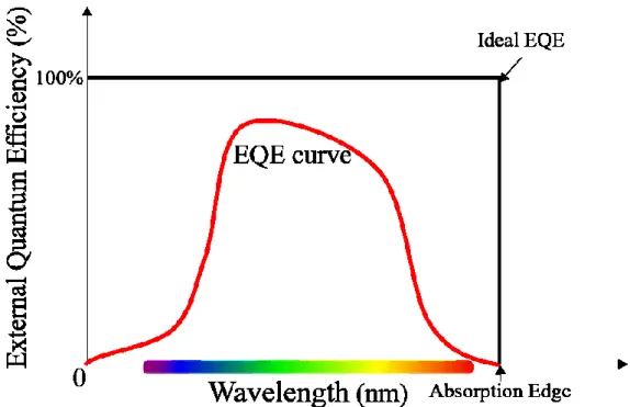
Another important evaluation for photovoltaics is the external quantum efficiency (EQE).
Quantum efficiency is the ratio of the number of carriers generated by the PV to the number of photons of a given energy incident on the PV. A typical EQE measurement is shown in Figure 1.2.1.4. An ideal curve would have 100% EQE starting from the absorption edge corresponding to the bandgap energy of the material. However, this is not possible due to several practical reasons such as charge recombination, scattered carriers, reduced absorption at long wavelengths due to low penetration depth, and low diffusion length. Since the number of
Figure 1.2.1.4. A typical EQE curve of a photovoltaic device.
14
carriers collected is related to the current density of a PV, the relationship between EQE and short-circuit current can be express as[58],
𝐸𝑄𝐸 =
1240×
𝐽𝐸
× 100 (1.2.3) where E
λ(W cm
−2) is the intensity of the monochromatic light and J
λis short-circuit current density at a given monochromated light irradiation with a wavelength of λ. In other words, since EQE refers to the number of electron-hole pairs successfully collected per incident photon, it evaluates the combined efficiency of light absorption, charge transport, and charge collection.
A closer measured EQE curve to the ideal EQE is preferable, which would mean a high ratio of charge collection per incident photon.
In 1960, Shockley et al. described the detailed balance limit of efficiency of p-n junction
solar cells.[59] The upper theoretical limit was then known to highly dependable on the light
Figure 1.2.1.5 Theoretical Shockley-Queisser limit of single heterojunction PV according to
bandgap energy.
15
absorbing layer’s bandgap energy.[60] The relationship between the bandgap energy and maximum theoretical power conversion efficiency (PCE) of PVs with a single heterojunction is shown Figure 1.2.1.5. From this figure, both copper oxides are at favorable positions near the peak of the curve, with maximum theoretical PCE of 30% and 20% for CuO and Cu
2O respectively. This indicates the promising potential these copper oxides possess.
The current records for Cu
2O PVs are PCE of 8.1% by thermal preparation[61], and 1.28% by electrodeposition reported by Izaki et al.[62]. Little research regarding CuO photovoltaics has been published, with very poor PCE values[63,64]. The reasons for the low PCE are not known presently. One may argue that CuO has a preferable bandgap energy compared to Cu
2O since a low bandgap is desirable and that a single-bandgap CuO PV is sufficient. While this might be true theoretically, this is not the case practically. One single bandgap solar cell cannot properly match the broad solar spectrum. Photons with energy lesser than the bandgap are not absorbed, and photons with energy larger than the bandgap generate electron-hole pairs which immediately lose almost all energy in excess of the bandgap energy[65], leading to a high thermal energy loss consequently. Additionally, the relationship between bandgap energy E
gand open-circuit voltage V
OC, as shown in the following equation[66],
𝑞𝑉
𝑂𝐶≅ 𝐸
𝑔
𝐶+ k𝑇
𝑐𝑙𝑛 {(
𝑆𝑜
) (
𝑇𝑆𝑇𝑐
) (
𝑆1𝑐1
)} (1.3)
where k is Boltzmann’s constant, q is the electronic charge, T
Sand T
care the sun (6000 K) and the cell (300 K) temperatures, respectively.
𝐶is the Carnot efficiency and
𝑆1,
𝑐1are correction terms.[67–69] And since the E
gand V
OCare directly related, E
gcan be considered as the upper limit to the extractable voltage from the cell.[70,71] As such, a single, low bandgap light-absorbing layer would have a lower maximum achievable V
OC.
Thus, some solar cells utilize a strategy to harvest multiple portions of the solar spectrum
which can overcome the solar cell limits by having different bandgap energies as the light-
16
absorbing layers. The multi-junction solar cell,[56,72,73] which contains two or more p-n
junctions made of different semiconductor materials produce electric current in response to
different wavelengths of light due to different bandgap energies. Another example is the
quantum dot solar cell,[27] which possesses tunable bandgap energies by varying particle size
and shape, and can even make infrared energy accessible[74]. Such a strategy of multiple
bandgaps incorporation might be applicable for the copper oxide photovoltaic as well, which
will be further discussed.
17
1.3 Strategy to Improve the Copper Oxide Based PV from EQE
From the fundamental understanding of the solid-state physics thus far, the respective factors can be improved by optimizing the fabrication process of the copper oxide based PV, in order to achieve the ultimate improvement in PCE. From the EQE, an overall improvement of the PV can be attempted in two ways:
1. Increase the overall values of the EQE curve.
2. Increase the absorption wavelength span, which means extending the absorption edge towards longer wavelength.
The first way can be achieved by attempting to improve the light-absorbing layer by lessening the defects and improve the electrical properties, which may lead to an improvement in charge collection. As such, morphology and microstructural characterization is important which might give insights to the quality of the light-absorbing layer, along with characterization of the electrical properties. In short, exploring ways to lessen defects and improve the semiconductor quality is the strategy to increase the overall values of the EQE. For Cu
2O, annealing is a common way to improve the layer quality for the Cu
2O. However, the extent of improvements and mechanism should be elucidated. For CuO, a large surface irregularity can occur corresponding to the increase in the heterointerface due to its morphology, and lessening the surface irregularity can improve the layer quality.
The second way can be attempted by utilizing both copper oxides, Cu
2O and CuO, with
different bandgap energies. The corresponding absorption edge for Cu
2O with a 2.1 eV bandgap
energy is approximately 650 nm, while a CuO layer with 1.45 eV is approximately 850 nm. As
discussed earlier, combining both copper oxides with different bandgap energies is a good
strategy to harvest a different portion of the sunlight spectrum. This may extend the absorption
edge and subsequently increase the EQE. In fact, the strategy of having different bandgaps has
been deployed in PVs to overcome the theoretical PCE such as CIGS[75,76] and quantum dots
PV[27,58]. Since Cu
2O and CuO have a eutectic system, it has been demonstrated by Izaki et
18
al. that by oxidizing the topmost Cu
2O layer by annealing in air in low temperature, a directly
stacked Cu
2O/CuO layer can be fabricated with a clear boundary, while retaining lattice
relationship.[77] This method will allow a combination of both copper oxides as the light-
absorbing layer. At the same time, when combining different light-absorbing materials, a proper
investigation is needed with respect to the band alignment. Band alignment can give insight to
the band offsets and charge transport mechanism[78–81], and an optimum band alignment can
be proposed based on its study. This calls for an investigation for the band alignment of the
combined copper oxides PV.
19
1.4 Research Objective
External quantum efficiency (EQE) is of high importance since it reflects on the overall photovoltaic performance in terms of absorption span of the solar spectrum and charge collection. To improve the EQE performance of the copper oxide based photovoltaics, this thesis explored methods to increase the EQE of the copper oxide PVs, in order contribute to improving the performance of copper oxide PVs as an excellent ultra-low cost Metal Oxide PV as the next-generation photovoltaics. Single Cu
2O-only PV was investigated, followed by CuO- only PV, and then directly stacked Cu
2O/CuO. The energy state of the PV was also investigated to facilitate the understanding of the copper oxide based PV. As such, the research objectives of this thesis are as follows,
To investigate the fabrication of the Cu
2O-only PV (GZO/ZnO/Cu
2O) by electrodeposition and elucidate the effects of annealing on the microstructural, electrical and EQE properties.
To investigate the fabrication of the CuO-only PV (CuO/Polysiloxane/GZO) by electrodeposition and IV evaluation to determine the possibility of CuO as a light absorbing layer.
To investigate the fabrication of directly stacked copper oxides (GZO/Cu
2O/CuO)
photoactive layer prepared by electrodeposition and annealing, and their EQE
properties as the absorbing layer.
20
To investigate the band alignment of the directly stacked copper oxide photoactive layer by XPS characterization to propose an improved band alignment
The overall objective of this thesis is to investigate methods of improving the EQE and
subsequently give insights and proposals to further improve the overall performance of the
copper oxide based photovoltaics and photoactive layer.
21
1.5 Outline of This Study
In this thesis, we study the fabrication of copper oxides (Cu
2O, CuO, and Cu
2O/CuO) photovoltaics and photoactive layer and investigate methods to increase the metal oxide PV performances, implied from its solid-state physics. The study from the fabrication of simple Cu
2O PVs by electrodeposition, then CuO PVs by electrodeposition and finally Cu
2O/CuO photoactive layer by annealing electrodeposited Cu
2O layer in air. At the same time of exploring the methods to increase the copper oxide based PV performances, this thesis studies and identifies the limiting factors and problems, which will prove useful in future advances for such ultra-low cost metal oxide thin film PVs.
Chapter 2 covers fabrication of ZnO/Cu
2O PV on transparent soda lime glass/Ga:ZnO substrate by electrodeposition. The electrodeposited devices were then annealed in RTA in different temperatures ranging from 423 K to 573 K in vacuum. The morphology and structure of the as-deposited and annealed ZnO/Cu
2O PV were characterized by field emission scanning electron microscope observation (FE-SEM) and X-ray Diffraction Pattern (XRD). The optical properties were investigated by ultraviolet-visible spectroscopy (Uv-vis), and the electrical properties were evaluated by Hall measurement, current-voltage measurement (I-V) and the external quantum efficiency (EQE). Cu
2O functions as the light-absorbing layer as expected, and an optimum increase of the maximum value of EQE to nearly 100% was achieved around 410 nm after annealing at 423 K, and the mechanism is discussed. The increase in EQE was also related to a successful improvement in PEC in terms of J
SC.
Chapter 3 discusses the fabrication of CuO/Polysiloxane/GZO PV on Au coated Si wafer
substrate. Electrodeposition was used to fabricate the CuO and the polysiloxane layer was
prepared by spin coating. Infrared spectra were recorded along with the observation of FE-SEM
and I-V evaluation. PV characteristics such as V
OC,J
SC,and FF were obtained at 0.24 V, 0.067
µA cm
–2and 0.29 respectively and this demonstrated that CuO successfully acted as the light-
22
absorbing layer, although showing room for improvements. The particularly high V
OCwas attributed the Polysiloxane buffer layer.
Chapter 4 describes the study of directly stacked copper oxides (GZO/Cu
2O/CuO) photoactive layer prepared by electrodeposition, followed by annealing in air. Similar characterization was carried out such as the investigation of the morphology and structure of the as-deposited GZO/Cu
2O and annealed GZO/Cu
2O/CuO by field emission scanning electron microscope observation (FE-SEM) and X-ray Diffraction Pattern (XRD). The optical properties were investigated by ultraviolet-visible spectroscopy (Uv-vis), followed by the external quantum efficiency (EQE). EQE of samples prepared at 523 K was further investigated under different low reversed biased voltages were also investigated to explain the directly stacked Cu
2O/CuO behavior. An extended absorption edge was achieved from 650 nm that of a Cu
2O layer to 850 nm of a CuO layer with both layers acting as the light absorbing layers under bias voltage at 523 K.
Chapter 5 describes the detailed X-ray photoelectron spectroscopy (XPS) examination of the Cu
2O-only and the directly stacked Cu
2O/CuO layer prepared under different conditions (temperatures). Characterization techniques including Auger Parameter and the Wagner Plot were deployed and the comparison to reported values of CuO and Cu
2O were made. A band diagram is drawn according to the XPS measurement and the optical bandgap calculated, and the behavior of the EQE shown in the previous chapter is explained. An improved bandgap is proposed based on the results.
And finally, Chapter 6 summarizes the results obtained and concludes this thesis.
23
REFERENCES
[1] K.L. Denman, G. Brasseur, A. Chidthaisong, P. Ciais, P.M. Cox, R.E. Dickinson, D.
Hauglustaine, C. Heinze, E. Holland, D. Jacob, U. Lohmann, S. Ramachandran, P.L. da S. Dias, S.C. Wofsy, X. Zhang, Chapter 7 - Couplings between changes in the climate system and biogeochemistry, Clim. Chang. 2007 Phys. Sci. Basis. (2007).
[2] G.A. McKinley, A.R. Fay, T. Takahashi, N. Metzl, Convergence of atmospheric and North Atlantic carbon dioxide trends on multidecadal timescales, Nat. Geosci. 4 (2011) 606–610. doi:10.1038/ngeo1193.
[3] UNFCCC, Paris Agreement, United Nations Framew. Conv. Clim. Chang. (2016).
doi:FCCC/CP/2015/L.9.
[4] T.N. Palmer, Climate extremes and the role of dynamics, Proc. Natl. Acad. Sci. 110 (2013) 5281–5282. doi:10.1073/pnas.1303295110.
[5] A.E. Cahill, M.E. Aiello-Lammens, M.C. Fisher-Reid, X. Hua, C.J. Karanewsky, H.
Yeong Ryu, G.C. Sbeglia, F. Spagnolo, J.B. Waldron, O. Warsi, J.J. Wiens, How does climate change cause extinction?, Proc. R. Soc. B Biol. Sci. 280 (2012) 20121890–
20121890. doi:10.1098/rspb.2012.1890.
[6] P.P. Wong, I.J. Losada, J.P. Gattuso, J. Hinkel, A. Khattabi, K.L. McInnes, Y. Saito, A.
Sallenger, R.J. Nicholls, F. Santos, S. Amez, Coastal Systems and Low-Lying Areas, in:
C.B. Field, V.R. Barros, D.J. Dokken, K.J. Mach, M.D. Mastrandrea (Eds.), Clim. Chang.
2014 Impacts, Adapt. Vulnerability, Cambridge University Press, Cambridge, 2015: pp.
361–410. doi:10.1017/CBO9781107415379.010.
[7] A.E. Raftery, A. Zimmer, D.M.W. Frierson, R. Startz, P. Liu, Less than 2 °C warming by 2100 unlikely, Nat. Clim. Chang. 7 (2017) 637–641. doi:10.1038/nclimate3352.
[8] W.C. Turkenburg, J. Beurskens, A. Faaij, P. Fraenkel, I. Fridleifsson, E. Lysen, D. David
Mills, J.R. Moreira, L. J. Nilsson, A. Schaap, W. C. Sinke, Renewable Energy
Technologies, in: D.. Communications Development Incorporated, Washington (Ed.),
24
World Energy Assess. Energy Chall. Sustain., September, United Nations Development Programme Bureau for Development Policy, United States of America, 2000: pp. 219–
267.
[9] C. Philibert, Solar Energy Perspectives, OECD, 2011. doi:10.1787/9789264124585-en.
[10] Bp, BP Statistical Review of World Energy 2018, 2018.
https://www.bp.com/content/dam/bp/en/corporate/pdf/energy-economics/statistical- review/bp-stats-review-2018-renewable-energy.pdf.
[11] NREL, Best Research-Cell Efficiencies, 2018.
doi:https://www.nrel.gov/pv/assets/pdfs/pv-efficiencies-07-17-2018.pdf.
[12] K. Branker, M.J.M. Pathak, J.M. Pearce, A review of solar photovoltaic levelized cost of electricity, Renew. Sustain. Energy Rev. 15 (2011) 4470–4482.
doi:10.1016/j.rser.2011.07.104.
[13] P.J. Reddy, Solar Power Generation: Technology, New Concepts & Policy, CRC Press, 2012. https://books.google.com/books?id=9mTGmlbwyvQC&pgis=1.
[14] NEDO, PV2030+ Abstract, (2008). https://www.nedo.go.jp/content/100080327.pdf.
[15] T. Inaba, E. Kobayashi, Y. Suwazono, M. Uetani, M. Oishi, H. Nakagawa, K. Nogawa, Estimation of cumulative cadmium intake causing Itai-itai disease, Toxicol. Lett. 159 (2005) 192–201. doi:10.1016/j.toxlet.2005.05.011.
[16] H. Baba, K. Tsuneyama, M. Yazaki, K. Nagata, T. Minamisaka, T. Tsuda, K. Nomoto, S. Hayashi, S. Miwa, T. Nakajima, Y. Nakanishi, K. Aoshima, J. Imura, The liver in itai- itai disease (chronic cadmium poisoning): Pathological features and metallothionein expression, Mod. Pathol. 26 (2013) 1228–1234. doi:10.1038/modpathol.2013.62.
[17] J. Pan, J.A. Plant, N. Voulvoulis, C.J. Oates, C. Ihlenfeld, Cadmium levels in Europe:
implications for human health., Environ. Geochem. Health. 32 (2010) 1–12.
doi:10.1007/s10653-009-9273-2.
25
[18] G. Bertin, D. Averbeck, Cadmium: cellular effects, modifications of biomolecules, modulation of DNA repair and genotoxic consequences (a review), Biochimie. 88 (2006) 1549–1559. doi:10.1016/j.biochi.2006.10.001.
[19] J.S. Manser, J.A. Christians, P. V. Kamat, Intriguing Optoelectronic Properties of Metal Halide Perovskites, Chem. Rev. 116 (2016) 12956–13008.
doi:10.1021/acs.chemrev.6b00136.
[20] A. Hagfeldt, G. Boschloo, L. Sun, L. Kloo, H. Pettersson, Dye-sensitized solar cells., Chem. Rev. (2010). doi:10.1002/chem.201101923.
[21] R. Ameta, S. Benjamin, S. Sharma, M. Trivedi, Dye-sensitized solar cells, in: Sol.
Energy Convers. Storage Photochem. Modes, 2015. doi:10.1201/b19148.
[22] G. Divitini, S. Cacovich, F. Matteocci, L. Cinà, A. Di Carlo, C. Ducati, In situ observation of heat-induced degradation of perovskite solar cells, Nat. Energy. 1 (2016) 15012. doi:10.1038/NENERGY.2015.12.
[23] S.K. Pathak, A. Abate, T. Leijtens, D.J. Hollman, J. Teuscher, L. Pazos, P. Docampo, U.
Steiner, H.J. Snaith, Towards long-term photostability of solid-state dye sensitized solar cells, Adv. Energy Mater. 4 (2014). doi:10.1002/aenm.201301667.
[24] S. Rühle, A.Y. Anderson, H.-N. Barad, B. Kupfer, Y. Bouhadana, E. Rosh-Hodesh, A.
Zaban, All-Oxide Photovoltaics, J. Phys. Chem. Lett. 3 (2012) 3755–3764.
doi:10.1021/jz3017039.
[25] T. Dittrich, A. Belaidi, A. Ennaoui, Concepts of inorganic solid-state nanostructured solar cells, Sol. Energy Mater. Sol. Cells. (2011). doi:10.1016/j.solmat.2010.12.034.
[26] S. Rühle, M. Shalom, A. Zaban, Quantum-dot-sensitized solar cells, ChemPhysChem.
(2010). doi:10.1002/cphc.201000069.
[27] P. V Kamat, Quantum Dot Solar Cells. The Next Big Thing in Photovoltaics.
doi:10.1021/jz400052e.
26
[28] S.Y. Yang, L.W. Martin, S.J. Byrnes, T.E. Conry, S.R. Basu, D. Paran, L. Reichertz, J.
Ihlefeld, C. Adamo, A. Melville, Y.H. Chu, C.H. Yang, J.L. Musfeldt, D.G. Schlom, J.W.
Ager, R. Ramesh, Photovoltaic effects in BiFeO3, Appl. Phys. Lett. (2009).
doi:10.1063/1.3204695.
[29] T. Choi, S. Lee, Y.J. Choi, V. Kiryukhin, S.W. Cheong, Switchable ferroelectric diode and photovoltaic effect in BiFeO3, Science (80-. ). (2009). doi:10.1126/science.1168636.
[30] H. Raebiger, S. Lany, A. Zunger, Origins of the p-type nature and cation deficiency in Cu
2O and related materials, Phys. Rev. B - Condens. Matter Mater. Phys. 76 (2007) 045209. doi:10.1103/PhysRevB.76.045209.
[31] M. Nolan, S.D. Elliott, The p-type conduction mechanism in Cu
2O: a first principles study, Phys. Chem. Chem. Phys. 8 (2006) 5350. doi:10.1039/b611969g.
[32] F.P. Koffyberg, F.A. Benko, A photoelectrochemical determination of the position of the conduction and valence band edges of p-type CuO, J. Appl. Phys. 53 (1982) 1173–1177.
doi:10.1063/1.330567.
[33] K. Nakaoka, J. Ueyama, K. Ogura, Photoelectrochemical Behavior of Electrodeposited CuO and Cu
2O Thin Films on Conducting Substrates, J. Electrochem. Soc. 151 (2004) C661. doi:10.1149/1.1789155.
[34] L. Wang, K. Han, M. Tao, Effect of Substrate Etching on Electrical Properties of Electrochemically Deposited CuO, J. Electrochem. Soc. 154 (2007) D91.
doi:10.1149/1.2404913.
[35] E.H. Kennard, E.O. Dieterich., An Effect of Light upon the Contact Potential of Selenium and Cuprous Oxide, Phys. Rev. 9 (1917) 58–63. doi:10.1103/PhysRev.9.58.
[36] T. Minami, Y. Nishi, T. Miyata, Heterojunction solar cell with 6% efficiency based on an n-type aluminum-gallium-oxide thin film and p-type sodium-doped Cu
2O sheet, Appl.
Phys. Express. 8 (2015) 022301. doi:10.7567/APEX.8.022301.
27
[37] T. Minami, Y. Nishi, T. Miyata, High-Efficiency Cu
2O-Based Heterojunction Solar Cells Fabricated Using a Ga
2O
3Thin Film as N-Type Layer, Appl. Phys. Express. 6 (2013) 044101. doi:10.7567/APEX.6.044101.
[38] Y. Ievskaya, R.L.Z. Hoye, A. Sadhanala, K.P. Musselman, J.L. MacManus-Driscoll, Fabrication of ZnO/Cu
2O heterojunctions in atmospheric conditions: Improved interface quality and solar cell performance, Sol. Energy Mater. Sol. Cells. 135 (2015) 43–48.
doi:10.1016/j.solmat.2014.09.018.
[39] S.W. Lee, Y.S. Lee, J. Heo, S.C. Siah, D. Chua, R.E. Brandt, S.B. Kim, J.P. Mailoa, T.
Buonassisi, R.G. Gordon, Improved Cu
2O-based solar cells using atomic layer deposition to control the Cu oxidation state at the p-n junction, Adv. Energy Mater. 4 (2014). doi:10.1002/aenm.201301916.
[40] T. Waechtler, N. Roth, R. Mothes, S. Schulze, E. Stefan, Copper Oxide ALD from a Cu(I) Beta-Diketonate: Detailed Growth Studies on SiO2 and TaN, ECS Trans. 25 (2009) 277–287. doi:10.1149/1.3205062.
[41] S.H. Wee, P.S. Huang, J.K. Lee, A. Goyal, Heteroepitaxial Cu
2O thin film solar cell on metallic substrates, Sci. Rep. 5 (2015). doi:10.1038/srep16272.
[42] C.R. Iordanescu, D. Tenciu, I.D. Feraru, A. Kiss, M. Bercu, D. Savastru, R. Notonier, C.E.A. Grigorescu, Structure and morphology of Cu-oxides films derived from PLD processes, Dig. J. Nanomater. Biostructures. 6 (2011) 863–868.
[43] C.L. Kuo, R.C. Wang, J.L. Huang, C.P. Liu, C.K. Wang, S.P. Chang, W.H. Chu, C.H.
Wang, C.H. Tu, The synthesis and electrical characterization of Cu2O/Al:ZnO radial p-
n junction nanowire arrays, Nanotechnology. 20 (2009). doi:10.1088/0957-
4484/20/36/365603.
28
[44] S. Jeong, E.S. Aydil, Heteroepitaxial growth of Cu
2O thin film on ZnO by metal organic chemical vapor deposition, J. Cryst. Growth. 311 (2009) 4188–4192.
doi:10.1016/j.jcrysgro.2009.07.020.
[45] S. Jeong, S.H. Song, K. Nagaich, S.A. Campbell, E.S. Aydil, An analysis of temperature dependent current–voltage characteristics of Cu
2O–ZnO heterojunction solar cells, Thin Solid Films. 519 (2011) 6613–6619. doi:10.1016/j.tsf.2011.04.241.
[46] Y.S. Lee, J. Heo, M.T. Winkler, S.C. Siah, S.B. Kim, R.G. Gordon, T. Buonassisi, Nitrogen-doped cuprous oxide as a p-type hole-transporting layer in thin-film solar cells, J. Mater. Chem. A. 1 (2013) 15416–15422. doi:10.1039/c3ta13208k.
[47] S. Noda, H. Shima, H. Akinaga, Cu2O/ZnO heterojunction solar cells fabricated by magnetron-sputter deposition method films using sintered ceramics targets, in: J. Phys.
Conf. Ser., 2013. doi:10.1088/1742-6596/433/1/012027.
[48] K. Akimoto, S. Ishizuka, M. Yanagita, Y. Nawa, G.K. Paul, T. Sakurai, Thin film deposition of Cu
2O and application for solar cells, Sol. Energy. (2006).
doi:10.1016/j.solener.2005.10.012.
[49] J. Gan, V. Venkatachalapathy, B.G. Svensson, E. V. Monakhov, Influence of target power on properties of CuxO thin films prepared by reactive radio frequency magnetron sputtering, in: Thin Solid Films, 2015: pp. 250–255. doi:10.1016/j.tsf.2015.05.029.
[50] A.T. Ravichandran, K. Dhanabalan, A. Vasuhi, R. Chandramohan, S. Mantha, Morphology, bandgap, and grain size tailoring in Cu
2O thin film by SILAR method, IEEE Trans. Nanotechnol. 14 (2015) 108–112. doi:10.1109/TNANO.2014.2369438.
[51] S. Chatterjee, S.K. Saha, A.J. Pal, Formation of all-oxide solar cells in atmospheric condition based on Cu
2O thin-films grown through SILAR technique, Sol. Energy Mater.
Sol. Cells. 147 (2016) 17–26. doi:10.1016/j.solmat.2015.11.045.
29
[52] B. Balamurugan, B.R. Mehta, Optical and structural properties of nanocrystalline copper oxide thin films prepared by activated reactive evaporation, Thin Solid Films. 396 (2001) 90–96. doi:10.1016/S0040-6090(01)01216-0.
[53] A.A. Ogwu, E. Bouquerel, O. Ademosu, S. Moh, E. Crossan, F. Placido, An investigation of the surface energy and optical transmittance of copper oxide thin films prepared by reactive magnetron sputtering, Acta Mater. 53 (2005) 5151–5159.
doi:10.1016/j.actamat.2005.07.035.
[54] L.C. Olsen, R.C. Bohara, M.W. Urie, Explanation for low-efficiency Cu
2O Schottky- barrier solar cells, Appl. Phys. Lett. 34 (1979) 47–49. doi:10.1063/1.90593.
[55] J. Kaur, O. Bethge, R.A. Wibowo, N. Bansal, M. Bauch, R. Hamid, E. Bertagnolli, T.
Dimopoulos, All-oxide solar cells based on electrodeposited Cu
2O absorber and atomic layer deposited ZnMgO on precious-metal-free electrode, Sol. Energy Mater. Sol. Cells.
161 (2017) 449–459. doi:10.1016/j.solmat.2016.12.017.
[56] H. Cotal, C. Fetzer, J. Boisvert, G. Kinsey, R. King, P. Hebert, H. Yoon, N. Karam, III–
V multijunction solar cells for concentrating photovoltaics, Energy Environ. Sci. 2 (2009) 174–192. doi:10.1039/B809257E.
[57] M.A. Green, Solar cell fill factors: General graph and empirical expressions, Solid State Electron. 24 (1981) 788–789. doi:10.1016/0038-1101(81)90062-9.
[58] I. Robel, V. Subramanian, M. Kuno, P. V. Kamat, Quantum Dot Solar Cells. Harvesting Light Energy with CdSe Nanocrystals Molecularly Linked to Mesoscopic TiO 2 Films, J. Am. Chem. Soc. 128 (2006) 2385–2393. doi:10.1021/ja056494n.
[59] W. Shockley, H.J. Queisser, Detailed balance limit of efficiency of p-n junction solar cells, J. Appl. Phys. 32 (1961) 510–519. doi:10.1063/1.1736034.
[60] S. Rühle, Tabulated values of the Shockley-Queisser limit for single junction solar cells,
Sol. Energy. 130 (2016) 139–147. doi:10.1016/j.solener.2016.02.015.
30
[61] T. Minami, Y. Nishi, T. Miyata, Efficiency enhancement using a Zn1-xGex-O thin film as an n-type window layer in Cu
2O-based heterojunction solar cells, Appl. Phys. Express.
9 (2016). doi:10.7567/APEX.9.052301.
[62] M. Izaki, T. Shinagawa, K.-T. Mizuno, Y. Ida, M. Inaba, A. Tasaka, Electrochemically constructed p-Cu 2 O/n-ZnO heterojunction diode for photovoltaic device, J. Phys. D.
Appl. Phys. 40 (2007) 3326–3329. doi:10.1088/0022-3727/40/11/010.
[63] R. Motoyoshi, T. Oku, H. Kidowaki, A. Suzuki, K. Kikuchi, S. Kikuchi, B. Jeyadevan, Structure and photovoltaic activity of cupric oxide-based thin film solar cells, J. Ceram.
Soc. Japan. 118 (2010) 1021–1023. doi:10.2109/jcersj2.118.1021.
[64] H. Kidowaki, T. Oku, T. Akiyama, Fabrication and characterization of CuO/ZnO solar cells, J. Phys. Conf. Ser. 352 (2012) 012022. doi:10.1088/1742-6596/352/1/012022.
[65] C.H. Henry, Limiting efficiencies of ideal single and multiple energy gap terrestrial solar cells, J. Appl. Phys. 51 (1980) 4494–4500. doi:10.1063/1.328272.
[66] A. Niv, Z.R. Abrams, M. Gharghi, C. Gladden, X. Zhang, Overcoming the bandgap limitation on solar cell materials, Appl. Phys. Lett. 100 (2012). doi:10.1063/1.3682101.
[67] Z.R. Abrams, A. Niv, X. Zhang, Solar energy enhancement using down-converting particles: A rigorous approach, J. Appl. Phys. 109 (2011). doi:10.1063/1.3592297.
[68] T. Markvart, Solar cell as a heat engine: Energy-entropy analysis of photovoltaic conversion, Phys. Status Solidi Appl. Mater. Sci. 205 (2008) 2752–2756.
doi:10.1002/pssa.200880460.
[69] W. Ruppel, P. Würfel, Upper Limit for the Conversion of Solar Energy, IEEE Trans.
Electron Devices. 27 (1980) 877–882. doi:10.1109/T-ED.1980.19950.
[70] M.A. Green, Limits on the Open-Circuit Voltage and Efficiency of Silicon Solar Cells Imposed by Intrinsic Auger Processes, IEEE Trans. Electron Devices. 31 (1984) 671–
678. doi:10.1109/T-ED.1984.21588.
31
[71] G.L. Araújo, A. Martí, Absolute limiting efficiencies for photovoltaic energy conversion, Sol. Energy Mater. Sol. Cells. 33 (1994) 213–240. doi:10.1016/0927-0248(94)90209-7.
[72] M. Yamaguchi, T. Takamoto, K. Araki, Super high-efficiency multi-junction and concentrator solar cells, Sol. Energy Mater. Sol. Cells. 90 (2006) 3068–3077.
doi:10.1016/j.solmat.2006.06.028.
[73] R.R. King, D.C. Law, K.M. Edmondson, C.M. Fetzer, G.S. Kinsey, H. Yoon, R.A. Sherif, N.H. Karam, 40% efficient metamorphic GaInPGaInAsGe multijunction solar cells, Appl. Phys. Lett. 90 (2007). doi:10.1063/1.2734507.
[74] E.H. Sargent, Infrared quantum dots, Adv. Mater. 17 (2005) 515–522.
doi:10.1002/adma.200401552.
[75] P. Jackson, D. Hariskos, E. Lotter, S. Paetel, R. Wuerz, R. Menner, W. Wischmann, M.
Powalla, New world record efficiency for Cu(In,Ga)Se2 thin-film solar cells beyond 20%, Prog. Photovoltaics Res. Appl. 19 (2011) 894–897. doi:10.1002/pip.1078.
[76] M.A. Contreras, L.M. Mansfield, B. Egaas, J. Li, M. Romero, R. Noufi, E. Rudiger- Voigt, W. Mannstadt, Wide bandgap Cu(In,Ga)Se2solar cells with improved energy conversion efficiency, Prog. Photovoltaics Res. Appl. 20 (2012) 843–850.
doi:10.1002/pip.2244.
[77] M. Izaki, K. Fukuzawa, Photovoltaic layer and the preparation process, 2017–54917, n.d.
[78] M. Yang, L. Zhu, Y. Li, L. Cao, Y. Guo, Asymmetric interface band alignments of Cu
2O/ZnO and ZnO/Cu 2O heterojunctions, J. Alloys Compd. (2013).
doi:10.1016/j.jallcom.2013.05.033.
[79] S. Siol, J.C. Hellmann, S.D. Tilley, M. Graetzel, J. Morasch, J. Deuermeier, W.
Jaegermann, A. Klein, Band Alignment Engineering at Cu
2O/ZnO Heterointerfaces,
ACS Appl. Mater. Interfaces. 8 (2016) 21824–21831. doi:10.1021/acsami.6b07325.
32
[80] H. Wei, H. Gong, Y. Wang, X. Hu, L. Chen, H. Xu, P. Liu, B. Cao, Three kinds of Cu
2O/ZnO heterostructure solar cells fabricated with electrochemical deposition and their structure-related photovoltaic properties, CrystEngComm. 13 (2011) 6065–6070.
doi:10.1039/c1ce05540b.
[81] Z. Kang, X. Yan, Y. Wang, Z. Bai, Y. Liu, Z. Zhang, P. Lin, X. Zhang, H. Yuan, X.
Zhang, Y. Zhang, Electronic Structure Engineering of Cu 2 O Film/ZnO Nanorods Array
All-Oxide p-n Heterostructure for Enhanced Photoelectrochemical Property and Self-
powered Biosensing Application, Sci. Rep. 5 (2015). doi:10.1038/srep07882.
33
CHAPTER 2
Fabrication of basic Cu
2O-only (GZO/ZnO/Cu
2O) PV and the Effects of Annealing on the EQE and PV Performances
2.1 Introduction
2.1.1 Electrodeposition of Cu
2O and ZnO
Electrodeposition is a major synthetic tool for the production of a large variety of
inorganic materials, such as oxides, hydroxides, phosphates, chalcogenides, as well as metals
and metal alloys.[1,2] Not only does it offer ease of thickness and morphology control, but it is
also feasible of large-scale, low-cost production.[3]
34
Early electrodeposition of Cu
2O from an alkaline bath was first developed by Stareck et al. in 1943[4], and the photovoltaic properties further studied in 1986 by Rakhshani et al.[5]
Cu
2O can be electrodeposited from alkaline electrolyte which contains cupric ions.[6,7] Lactate is one of stabilizing agent to form soluble copper lactate complex in the electrolyte, and the predominant complex is Cu(II)Lac
2[8], and the formation of Cu
2O takes place in a two-step process given by the following reactions, [9]
Cu(II)Lac
2+ e
–↔ Cu(I)Lac + Lac
–2Cu(I)Lac + 2OH
–↔ Cu
2O + H
2O + 2Lac
–And electrodeposition of Cu
2O can also be carried out in weak acid without reduction to copper metal if OH
–ion from dissolved oxygen is present.[10]
In 1995, the first preparation of transparent ZnO films with characteristic optical band gap energy of 3.3 eV by electrodeposition from aqueous electrolyte was reported by Izaki et al.[11] And a subsequent successful heteroepitaxial electrodeposition of ZnO/Cu
2O forming a photovoltaic device by the same group has achieved 1.28% in PCE.[7] Not only did this strongly demonstrate the room for improvement for the electrodeposited Cu
2O-based PV, but it also prompted the need for a clear understanding of the factors limiting the cell performance fabricated by electrodeposition.
2.1.2 Annealing
The effects on annealing have been known to improve the qualities of a layer, and annealing in air/vacuum on the Cu
2O layers with varying results have been reported.
Mahalingam et al. reported that the best result was obtained when sample prepared by
electrodeposition at pH 9 solution was annealed in air at 623 K with the highest increase in
peak height of (200) cubic phase and increase in grain size to 100 nm. [12] Liang et al. reported
that the best photoelectrochemical current obtained was from Cu
2O film electrodeposited at pH
35
9 with 60 minutes of annealing at 623 K in Ar atmosphere.[13] Dimopoulos et al. reported that the best result was obtained when the sample prepared by electrodeposition at pH 12.5 was annealed in vacuum at 573 K, with highest open-circuit voltage (V
OC= 0.51 V), short-circuit current (J
SC= 4.67 mA cm
−2), and conversion efficiency (η =1.12%) respectively, but with linear I-V characteristics appearing when annealed at 623 K.[14] Hsieh et al. reported that the best result was obtained when the sample was prepared by DC-reactive magnetron sputtering at 473 K were annealed at 823 K with 1.2% oxygen added in the protective annealing atmosphere, possessing the lowest resistivity, but the rectifying effect of P-N junction disappeared.[15] Despite the similarity in positive results achievable after annealing, there is a discrepancy regarding the optimum temperature. Also, discussions about the disappearance of the rectifying effect after optimum annealing conditions were lacking. So the mechanisms and origin of the effects and improvements by annealing on photovoltaic devices were still obscure and the explanation insufficient. Little effort has been done to investigate the importance in microstructural change which offers insight and direct evidence to the changes of the light- absorbing Cu
2O-layer and the phase transitions when annealed.
In a previous study by Shinagawa et al., significant improvements in the photoelectric
performances were achieved in Cu
2O-only layer after annealing.[16] This chapter applies the
similar concept in the constructed ZnO/Cu
2O device, and focus on the most important aspects
of improvements while paying attention to the microstructural changes when annealed in
vacuum, which offer further explanations to the discrepancy between mentioned reports, and
further insight into the mechanism of annealing.
36
2.2 Experimental Procedures
2.2.1 Preparation of ZnO/Cu
2O PVs
ZnO was electrodeposited on conductive gallium-doped zinc oxide (GZO)-coated glass
substrate. Prior to the electrodeposition, the GZO substrate was rinsed with acetone, degreased
in 0.1 mol L
–1NaOH and rinsed with deionized water. ZnO was then deposited
potentiostatically at −0.8 V referenced to an Ag/AgCl electrode in saturated KCl, [11] at an
electric charge of 0.02 C cm
–2with a potentiostat (Hokuto Denko, HAL-3001), connected to a
Coulomb meter (Hokuto Denko, HF-301) in an aqueous solution of 8 mmol L
–1zinc nitrate
hexahydrate (Zn(NO
3)
2・6H2O, Nacalai Tesque, Inc.) at 336 K. A Pt plate was used as the
counter electrode. Cu
2O was then electrodeposited on the ZnO layer from an alkaline aqueous
solution (pH = 12.5) containing 0.4 mol L
–1copper (II) acetate monohydrate (Cu(CH
3COO)
2・H2O, Nacalai Tesque, Inc.) and 3 mol L
–1lactic acid (Kanto Chemical, Co., Inc.). The pH was
adjusted with NaOH. This electrodeposition was carried out at −0.4 V and at an electric charge
of 1.7 C cm
–2at 313 K without stirring. All aqueous solutions used here were prepared with
deionized water purified by an Elix-UV system (Millipore). The schematics of the structure of
PV is shown in Figure 2.2.1.
37
![Figure 1.1.1 Top countries with cumulative installed capacity of PVs by Year.[10]](https://thumb-ap.123doks.com/thumbv2/123deta/10127123.1961048/13.892.134.783.119.443/figure-countries-cumulative-installed-capacity-pvs-year.webp)