Waseda University Doctoral Dissertation
Study on High Efficiency CMOS Rectifiers for Energy Harvesting and
Wireless Power Transfer Systems
Qiang LI
Graduate School of Information, Production and Systems Waseda University
June 2015
The field of vibration energy harvesting and wireless power transfer technologies are growing rapidly in recent years, which are largely stimulated by the advances of different researches, such as piezoelectronic vibration harvester and biomedical implant devices.
They play a more and more important role in renewable resources and sensor systems.
Among the components constituting the two systems, rectifier as the interface circuit is a critical part and it is quite significant to promote their performances.
Rectifier in vibration energy harvesting system is utilized to change the AC power generated by piezoelectronic generator to DC one. Commonly, the typical working frequency of the generator is from mHz to kHz. Conventional rectifiers consisting of diode-connected transistors in CMOS integrated circuits are not suitable for this application considering the big forward voltage drop and poor efficiency. The output voltage amplitude of different micro harvesting generators may vary and output voltage and power are usually low. Therefore, both low power, low voltage and wide input voltage amplitude range are needed for the rectifier in vibration energy harvesting system. By using the bulk-driven comparator technique, a paper published in TCAS2011 reduced the minimum operation voltage to 0.5 V. Another research in NOLTA2012 further improved the minimum input voltage to as small as 0.3 V with similar concept. Both researches filled the rectifiers gap in the field of low voltage energy harvesting system. However, the drawbacks of the bulk- driven techniques are also obvious. Body diode is easily to be turned on when reverse voltage is larger than 0.7 V. This phenomenon decides that the maximum operation voltage of the rectifiers proposed in the above two papers are smaller than 1 V. Besides the energy harvesting, rectifier for wireless power transfer is also a key research in the power transfer system, especially for the biomedical implant devices. In this case, the rectifier integrated in the receiver rectifies the signals and powers the implant device. The distance between two coils and the relative position of coils center influence the transfer efficiency. Far distance and the position mismatch result in small received voltage amplitude. Thus, minimum operation voltage of the rectifier should be as low as enough to avoid the influence caused by poor coupling.
On the other hand, higher performance of the rectifier means higher total efficiency.
Rectifier consisting of active diode for wireless power transfer was first proposed in ISCAS2005 to replace the conventional diode-connected MOS rectifiers. Comparator is used to control a switch, which works as an ideal diode without voltage drop. These active rectifiers are much frequency dependent. High frequency will result in reverse current if the control circuit cannot response quickly, which reducing the conversion efficiency. A 100 kHz, 1.2 V rectifier with reverse current consideration was first proposed in JSSC2009.
Considering the influence of poor coil coupling, the operation voltage is not small enough.
In the case of higher frequency of 13.56 MHz, both passive and active rectifiers can be used.
In the design of passive rectifiers, threshold voltage cancellation technology is commonly used (TBCAS2012). However, the utilization of capacitors increases chip area and all these circuits are investigated for low input signal applications, where current direction is not controlled. Though the active rectifier proposed in TCAS2012 can control the current direction, the time delay of the comparator with a common gate structure results in the reverse current and poor power efficiency. Basing on the above considerations and drawbacks of previous researches, three novel rectifier circuits that focus on different issues have been proposed in this dissertation, respectively.
The dissertation is organized with five chapters as follows.
In Chapter 1, the application background and different topologies of previous research- es are briefly introduced. Then the motivations and objective of this dissertation are presented based on the drawbacks of previous designs. The last section of this chapter is the organization of this dissertation.
In Chapter 2, a low voltage CMOS active rectifier is proposed. This structure is designed for transcutaneous power transmission in low power battery-less devices such as biomedical implants. By using a simple comparator-controlled switch that needs a small supply voltage, the lowest input voltage amplitude can be reduced to 0.7 V with a standard CMOS 0.18 µm process, which is much smaller than 1.2 V in previous researches. Comparing with traditional diode bridge structure, the proposed rectifier uses only one comparator and a negative voltage converter. This proposed design dramatically
reduces the power loss. In combination with current offset bias circuit, the reverse current of the rectifier under different input amplitudes is minimized. The proposed circuit is measured with an input source frequency from 100 kHz to 1.5MHz and a load of 500 Ω. The measurement results show that the proposed rectifier can achieve a maximum peak voltage conversion efficiency of more than 88% and a power efficiency of approximately 86.5%. The performances are improved comparing with the measured voltage conversion efficiency of 86% and simulated power efficiency of 87% in the paper of JSSC2009.
In Chapter 3, a wide input amplitude range and highly efficient CMOS rectifier for low power energy harvesting system is proposed. The working frequency is from 10 Hz to 1 kHz. Comparing with previous design with bulk-driven comparator, the proposed rectifier utilizes full bridge structure and source-driven comparator is used in the novel active diode.
Body diode is always reversely biased even the input voltage is higher than 1 V, which makes the rectifier work at a wide range of input voltage amplitudes of 0.45 V up to 1.8 V under a standard 0.18 µm CMOS process. The comparator that consists of common- gate stage and control stage is biased to weak inversion region to control the switch of the active diode. This technology reduces the minimum operation voltage to as low as 0.45 V.
The proposed rectifier can achieve a peak voltage conversion efficiency of over 96% and a power efficiency over 90% with a load value of 50 kΩ. Simulated power consumption of the rectifier is 264.35 nW with a 500 mV input, which is about 30% smaller than the best recently published results (TCAS2011). The power transistors used in the rectifier are only 1/3 of the previous design. Smaller transistors result in better efficiency and help to save the chip area.
In Chapter 4, a 1 V, high efficiency comparator-based CMOS rectifier for wireless power transfer in biomedical applications is presented. A novel active diode controlled by a cross-coupled comparator is designed to overcome the common-mode voltage limit of traditional structure and improve the conversion efficiency. Reverse current is also reduced by utilizing a switch off response compensation technique considering the charge delay caused by large gate-capacitor of the switch transistors and high frequency. The switch off response compensation technique can not only reduce the reverse current but also maximize
the conduction time of the active diode by using a SR latch circuit. The proposed rectifier is verified using a standard 0.18µm CMOS process with an input source frequency of 13.56 MHz. Results show that the rectifier can achieve a maximum voltage conversion efficiency of 92% and power efficiency about 86% with a load value of 500 Ω. Simulated power consumption of the rectifier is only 0.259 mW with a 1 V peak input voltage. Though the minimum operation voltage in previous paper can be as low as 0.8 V by using Vth cancellation technology, the voltage efficiency is only 37.5% even with a light load of 2 kΩ.
In Chapter 5, the conclusions of this dissertation are given.
Contents
Abstract i
List of Tables ix
List of Figures xi
1 Introduction 1
1.1 Background . . . 1
1.1.1 Rectifier devices and circuits . . . 1
1.1.2 Rectifier applications . . . 3
1.1.3 Topologies of previous researches . . . 6
1.2 Motivation and research objective of this dissertation . . . 17
1.3 Contribution of this dissertation and its organization . . . 18
2 Low voltage CMOS rectifier for low power battery-less devices 21 2.1 Introduction . . . 21
2.2 The principle of a negative voltage converter . . . 23
2.3 Proposed low voltage rectifier . . . 25
2.3.1 Low operation voltage active diode . . . 25
2.3.2 Reverse current consideration and current offset . . . 27
2.4 Simulation and measurement results . . . 31
2.4.1 Minimum input voltage and voltage conversion efficiency . . . 33
2.4.2 Power efficiency . . . 37
2.4.3 Performance in different process corners . . . 38
2.4.4 Performance in low frequency . . . 38
2.4.5 Performance comparisons . . . 41
2.5 Summary . . . 41
3 Wide input amplitude range rectifier for energy harvesting system 42 3.1 Introduction . . . 42
3.2 Rectifier topologies . . . 43
3.3 Proposed rectifier and design consideration . . . 45
3.3.1 Schematic and work principle . . . 45
3.3.2 Proposed control circuit . . . 46
3.3.3 Latch-up consideration . . . 48
3.3.4 Reverse current consideration . . . 50
3.4 Simulation and measurement results . . . 52
3.4.1 Input range and voltage conversion efficiency . . . 54
3.4.2 Power efficiency . . . 59
3.4.3 Working frequency . . . 60
3.4.4 Power consumption . . . 63
3.4.5 Corner simulation . . . 63
3.4.6 Performance comparisons . . . 64
3.5 Summary . . . 67
4 1V CMOS rectifier with response compensation for wireless power transfer 69 4.1 Introduction . . . 69
4.2 Rectifier topologies . . . 71
4.3 Circuit implementation and design considerations . . . 73
4.3.1 Operation principle . . . 73
4.3.2 Active diode design . . . 76
4.3.3 Reverse current consideration and current reference design . . . 79
4.4 Simulation results and considerations . . . 82
4.4.1 Switch off delay compensation and minimum operation voltage . . 84
4.4.2 Voltage conversion efficiency and power efficiency . . . 85
4.4.3 Performance in different corners . . . 90
4.4.4 Performance Comparison . . . 93
4.5 Summary . . . 94
5 Conclusions 95 5.1 Conclusions . . . 95
5.2 Future work . . . 97
Bibliography 99
Acknowledgements 109
Publications 111
List of Tables
2.1 Circuit transistor sizes. . . 30
2.2 Performance comparisons between rectifiers. . . 40
3.1 Circuit transistor sizes. . . 54
3.2 Power consumption. . . 63
3.3 Performance comparisons between rectifiers. . . 65
4.1 Output of SR latch with different MP1and MP2state. . . 82
4.2 Performance comparisons between rectifiers. . . 92
List of Figures
1.1 Half wave rectifier [1]. . . 2
1.2 Full wave rectifier [1]. . . 3
1.3 CMOS rectifier with diode configuration. . . 7
1.4 CMOS rectifier with cross-couple configuration. . . 8
1.5 Conceptual schematic of active diode [22]. . . 9
1.6 Schematic of bulk-input comparator [24]. . . 10
1.7 Schematic of negative voltage converter with body bias block [25]. . . 11
1.8 Four input comparator with RCC block in [26]. . . 12
1.9 Schematic of the proposed rectifier in [27]. . . 14
1.10 Unbalanced comparator in [27]. . . 14
1.11 Rectifier for UHF application based on negative voltage convertor [28]. . . 15
1.12 Vthcancellation rectifier in [30]. . . 16
2.1 Schematic of a power transmission system of biomedical implants. . . 21
2.2 Circuit diagram of the negative voltage converter [29]. . . 24
2.3 Simplified schematic of the proposed rectifier. . . 25
2.4 Circuit diagram of the proposed rectifier . . . 26
2.5 Output waveforms of the proposed rectifier with balanced transistor size. . . 28
2.6 Simulated waveforms using current offset when|Vin |peak=1.7V. . . 28
2.7 Simulated waveforms using current offset when|Vin |peak=0.7V. . . 29
2.8 Test circuit for chip measurement. . . 31
2.9 Micrograph of the proposed rectifier. . . 32
2.10 Simulated output voltage under 100 kHz, 0.7 V input with RL=500Ω. . . . 32
2.11 Simulated output voltage under 1.5 MHz, 0.7 V input with RL=500Ω. . . . 33
2.12 Measured output voltage under 100 kHz, 0.7 V input with RL=500Ω. . . . 34
2.13 Measured output voltage under 1.5 MHz, 0.7 V input with RL=500Ω. . . . 34
2.14 Simulated voltage conversion efficiency under different input amplitudes. . 35
2.15 Simulated voltage conversion efficiencies with a 100 kHz input frequency. . 35
2.16 Measured peak voltage conversion efficiency versus different input amplitudes 36 2.17 Measured peak voltage conversion efficiency with a 100 kHz input frequency 36 2.18 Simulated power efficiency versus different input amplitudes. . . 37
2.19 Measured power efficiency versus different input amplitudes. . . 38
2.20 Voltage conversion efficiency with low input source frequencies . . . 39
2.21 Power efficiency under low input frequencies . . . 39
3.1 Schematic of vibrational energy harvester circuit interface. . . 43
3.2 Conceptual schematic of the proposed rectifier. . . 45
3.3 Schematic of the proposed active diode. . . 47
3.4 Simulated waveform of the rectifier in steady-stage. . . 49
3.5 Simulated waveform of the rectifier in start-up state. . . 49
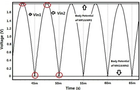
3.6 Simulated waveform of the [email protected] V and 100 Hz. . . 50
3.7 Simulated waveform of the [email protected] V and 100 Hz. . . 51
3.8 Simulated waveform of the [email protected] V and 100 Hz. . . 51
3.9 Simulated waveform of the [email protected] V and 100 Hz. . . 52
3.10 Schematic of the proposed rectifier. . . 53
3.11 Chip photograph of the fabricated rectifier. . . 55
3.12 Simulated steady-state of the proposed [email protected] V. . . 55
3.13 Measured steady-state of the proposed [email protected] V,10 Hz. . . 56
3.14 Measured steady-state of the proposed [email protected] V, 1 kHz. . . 57
3.15 Simulated voltage conversion efficiency @ 0-1.8V 100 Hz. . . 57
3.16 Measured voltage efficiency under different load conditions. . . 58
3.17 Simulated power efficiency @ 0-1.8V 100 Hz . . . 59
3.18 Measured power efficiency @ 0-1.8V 100 Hz . . . 60
3.19 Voltage conversion efficiency versus input voltage amplitude. . . 61
3.20 Power efficiency @0-1.8V 10 Hz-1 kHz . . . 61
3.21 Measured voltage conversion efficiency versus different amplitudes. . . 62
3.22 Measured power efficiency versus different amplitudes. . . 62
3.23 Voltage conversion efficiency comparison with previous published papers. . 66
3.24 Power efficiency comparison with previous published papers. . . 66
3.25 Output voltage ripple comparison with previous published papers. . . 67
4.1 Schematic of wireless power transmission system. . . 70
4.2 Conventional rectifier circuits. . . 71
4.3 Conceptual schematic of proposed rectifier circuit. . . 74
4.4 Circuit implementation of the comparatorC MP1. . . 77
4.5 Gain and hysteresis verification. . . 79
4.6 Waveform of signals from the proposedC MP1without any compensation. . 80
4.7 Comparator response with/without compensation. . . 81
4.8 Schematic of the bias current reference. . . 83
4.9 Chip micrograph of the proposed rectifier. . . 84
4.10 Simulated waveform with switch off delay compensation. . . 85
4.11 Measurement output voltage with an input voltage amplitude of 0.9 V. . . . 86
4.12 Simulated VE versus voltage amplitude. . . 86
4.13 Measured VE versus voltage amplitude. . . 87
4.14 Simulated power efficiency verse different input voltage amplitudes. . . 89
4.15 Measured power efficiency verse different input voltage amplitudes. . . 89
4.16 Power consumption composition of the proposed rectifier. . . 90
4.17 Voltage conversion efficiency and power efficiency verseRL. . . 91
4.18 Voltage conversion efficiency under different corners. . . 91
4.19 Power efficiency under different corners. . . 93
Chapter 1 Introduction
1.1 Background
1.1.1 Rectifier devices and circuits
A rectifier is an electrical and electronic device, which is widely utilized in different applications. The function of a rectifier is to convert AC (alternating current) source to DC (direct current) ones, which is known as rectification. The first generation of rectifier is made of vacuum tube diode and copper oxide metal. The two technologies were widely used before the development of semiconductor industry. With the development of semiconductor technology, the rectifier consisting of vacuum tube diode gradually fade out the market. The traditional rectifiers can only be found in some vacuum tube audio equipment. Instead, the semiconductor diode, such as p-n junction diode and schottky diode became popular in the power rectification applications of both low current and high current fields. With the development of integrated CMOS technology, the diode connected MOS transistors are widely used in integrated circuits in place of the discrete diode components.
Rectifiers can be divided into multi phase rectifier and single phase rectifier. Three phase (multi phase) rectifier circuits are very important for industrial application and high voltage DC energy transmission. However, most rectifiers for domestic equipment are
Figure 1.1: Half wave rectifier [1].
single phase, especially for low power, low voltage integrated circuits. Considering our research topics, we only focus on the single phase rectifier in this dissertation.
Single phase rectifiers can be divided into two types: half wave rectifier and full wave rectifier. For the half wave rectifier, the function of rectification is only available in the positive half cycle or negative half cycle, and the other cycle is blocked, which is shown in Fig. 1.1. These drawbacks decide that the average output voltage is not high, because half cycle of the input source is wasted and only one half is used to charge the output capacitor.
Half wave rectification requires a single diode in a single phase supply. The output voltage ripple of the half wave rectifier is larger than the full wave rectifier. Thus, there should be much more filtering techniques used in the output terminal to overcome the AC frequency harmonics.
A full wave rectifier converts the whole cycle of the input AC source to DC by using two conductive branches. Each branch rectifies one half of the whole cycle, but only one constant terminal is charged as its output. The function is shown in Fig. 2.2. The output voltage is much higher than the half wave type, because both the negative and positive waveforms are passed to the output and converted to direct current. That’s why the full wave rectifier structure is widely used in CMOS integrated circuits design.
Figure 1.2: Full wave rectifier [1].
1.1.2 Rectifier applications
The field of energy harvesting and wireless power transfer are two hot topics recently, which are stimulated by the advances of different researches [2], [3], [4], [5], [6], [7], [8].
In both applications, rectifiers play a very important role in the interface circuit to convert the AC sources to DC sources and power the load system. The performance and efficiency of the rectifier influence the system a lot.
Energy harvesting technology is the process by which energy is derived from external sources, such as solar power, thermal energy, wind energy, salinity gradients and kinetic energy. The power is captured and stored for small and wireless autonomous devices, like those used in wearable electronics and wireless sensor networks. Comparing with conventional battery power systems, energy harvesting device has a long lifetime and is widely used in the system which is difficult to access to. Besides the battery, the input fuel (oil, coal, etc) wasted by the large size generator is also un-ignored. Comparing with these limited sources, the energy source harvested from environment is free and ambient. For instance, the solar energy is ambient and can be harvested by the solar panel every day and vibration energy exists from operating engines and moving devices. Among different types of energy harvesting technologies [9], [10], [11], vibration energy harvesting technology attracts a great of interests by its widely applications. Vibration energy harvesting is well suited for technical environment, such as engines and railroad bridges. Commonly, vibration energy harvesters convert mechanical vibrational energy into alternating electrical energy, thus rectifier is needed to change the AC source to DC one, which can be used
to drive a multitude of load systems or recharge a battery. Moreover, the output voltage amplitude of different micro harvesting generators may vary and output power is usually low, therefore both efficiency and wide input amplitude range are needed for the rectifier design. Thus, the rectifier plays a very important role in the vibration energy harvesting circuit interface.
Wireless energy transmission or wireless power transfer technology is to transfer the power from a supply source to the consuming devices. The power is commonly transferred through coupling coils without using solid wire or conductor [12], [13]. There are a number of technologies for wireless power transfer. Most of them are using time varying electromagnetic field as the transmission mediums [13], [14], [15]. The development of wireless power transmission does a great help to the devices which are inconvenient to be powered by interconnecting wires, especially for the application of biomedical implant devices and monitoring devices in some severe environment.
Wireless power can be transferred and power one or more devices. Power source is commonly connected to the transmitter device. Coil in the transmitter transmits the power through the electromagnetic field across some intervening space to the coil in the receiver [15]. The transfer voltages or currents are alternating sources, which cannot directly power the load circuit.
Commonly, there are two types of wireless power techniques [16]: radiative and non radiative. The radiative technique is also called far field technique or power beaming.
Because the power is transferred through electromagnetic radiation like laser beam or microwave. The big merit of radiative technique is the longer transfer distances. However the energy should be aimed in the receiver. Wireless powered drone aircraft and solar power satellite are well known as the applications for radiative types. However, an unsolved issue for the radiative type still limits its application. For the longer transfer distance people and other living things exposure themselves to the potentially injurious electromagnetic field, which is a big risk to them. The other type of non radiative or near field techniques is commonly utilized in the power transmission for short distance. The energy is transferred by using inductive coupling coils or capacitive coupling electrodes through magnetic field
or electric field [17]. The applications of near field type are widely found in daily life, such as wireless charged cars, wireless toothbrush charger and RFID tag. This technique can be also utilized for implantable medical devices like implanted hearing-aid, heart pacemakers and blood flow monitor. Recently, most of researches focus on the wireless charge for these hand-held computing devices and implantable devices without tethered to the wall plug.
Among different applications of wireless power transfer technology, the development of implantable biomedical devices is enabled by the advances in the field of neural recording [18], cochlear implants [19], and blood flow sensing. Wireless power supply for implantable biomedical devices are very important, considering the critical issue of the consistent power supply, where stable and long life time power are two important factors.
Conventional power method of using a battery should be avoided due to the short life time, periodical replacement and large size, which is bad to human being’s healthy. By using the power transfer technology, sustained power can be supplied to the implant devices.
However power received by the receiver is commonly alternation source, rectifier is needed to convert the AC source to DC source. Rectified DC power is then supplied to the load circuit and charges the battery. Thus, the performance of the rectifier is very important in the whole system design due to several reasons:
1. Voltage efficiency: The rectifier converts the AC voltage supplied by the receiver to DC voltage and powers the load circuit. The voltage efficiency of the rectifier decides the output voltage. Higher efficiency means larger output voltage;
2. Minimum operation voltage: The rectifier used in the application must be self-biased.
The voltage received from the receiver is not only the rectified signal. The peak amplitude of the input source also influences the output voltage. As introduced in the above, inductive coupling between coils or capacitive coupling are the two main technologies for the near field applications. The distance between the two coils and the relative position of coil center influence the transfer efficiency. Farer distance of two coils and the position mismatch of the coil’s center result in small transfer voltage, which means the voltage amplitude received by the receiver will be
influenced a lot. Thus, a low voltage rectifier can cover the influence caused by the capacitive coupling or inductive coupling coils mismatch;
3. Power efficiency: Wireless power transmission system consists of power amplifier, inductive coil, rectifier and regulator. It is important to mention that the efficiency of the rectifier is usually the bottleneck. Higher power efficiency means higher total efficiency;
4. Working frequency: As introduced above, there are two categories of the wireless power techniques, near-field and radiative. The working frequency chosen for the system is also very important. The working frequency should not be too low considering of the coil’s size in the receiver if it is utilized in the biomedical implant devices. However, it should also not be too high for avoiding the potential hazards to human safety.
Based on the above considerations, rectifier plays a very important role in the application of energy harvesting system and wireless power transfer system. The performance of the rectifier decides the efficiency of the system.
1.1.3 Topologies of previous researches
The history of rectifier goes back to 1928. A device of electrolytic rectifier was patented by G. W. Carpenter in 1928 [20]. But it would be only suited to the use of low voltage applications, because the breakdown voltage of these rectifiers are very low and the electric shock is easy to happen, which is a big risk. With the development of semiconductor technology, discrete component was induced. Rectifiers achieved by diodes and capacitors were widely used. The half-wave rectifier consists of a single diode and very simple.
The full wave rectifier composed of diode bridge makes full use of the input source, because both the negative and positive period pass to the load. Thus, the output ripple is much smaller than the half wave rectifier. The diode structure rectifier is always used in high supply voltage field. However, it is seldom used in low voltage systems because
Figure 1.3: CMOS rectifier with diode configuration.
of the large forward voltage loss (typically 0.7 V-1 V), which cannot be accepted in low voltage integrated systems. Though schottky diode with a low forward voltage drop can replace the common diode to improve the voltage conversion efficiency, the high production cost and high reverse leakage current block its uses. Since integrated circuit is developing day by day, circuit designers try to implement different kinds of discrete components in the integrated circuits. In CMOS implementation circuits, discrete diode can be replaced by CMOS transistors in diode-connected configuration, which is given in Fig. 1.3. However, the voltage conversion and power efficiency are not sufficient because of the two diode forward voltage drops still exist. The voltage drop on each diode-connected MOS transistors is oneVGS and the minimumVGS can be reduced to oneVth( the threshold voltage ). Low threshold voltage transistor can be utilized to further reduce the operation voltage. However the additional masks and fabrication steps increase the process cost.
In [21], the author used a cross coupled structure to replace two semiconductor diodes of the diode-bridge structure, which is shown in Fig. 1.4. Input AC source is directly connected to the gate terminals to drive the NMOS transistors. When the input voltage amplitude is larger thanVth, one of the two NMOS transistors will be turned on depending on the input source phase. Two diode-connected transistors work as switches. They turn off to block the reverse current when input source amplitude is smaller than the output voltage
Figure 1.4: CMOS rectifier with cross-couple configuration.
and turn on when the input voltage amplitude is larger than the output voltage. By using the cross-couple structure, voltage drop is reduced because the voltage drop on each cross- coupled transistor is only one Vdsn. However, the two switches are still in diode structure connection and voltage loss still exists on each switch, thus the efficiency is not optimized for the voltage drop on the switch diode.
We call all the above rectifiers integrated passive rectifiers. The merit of these passive rectifiers is frequency independent, because the structure is simple and no other circuits are included. However, the voltage and power efficiency are commonly not sufficient because of the voltage drop on diode-connected MOS transistors. Though the cross-couple structure can reduce the voltage drop to only oneVth and low threshold voltage technology can be utilized to further reduce it,the passive rectifiers are still not suited for some low voltage applications. Sometimes, passive rectifiers are even the bottleneck of the whole system.
In order to overcome the drawbacks of above passive rectifiers and to further improve the voltage conversion efficiency and power efficiency. A concept of active diode was first proposed in [22] instead of the diode connected transistors in the conventional passive rectifiers. The active diode works as an ideal diode without voltage drop and reverse current. Figure 1.5 shows the conceptual schematic of the active diode [22]. It is composed
Figure 1.5: Conceptual schematic of active diode [22].
of a comparator and a transistor switch. It should be mentioned that the comparator should be powered by the output signal. When the input source amplitude is larger than the amplitude of output voltage, the comparator will turn on the switch and current flows from input source to the output terminal and charges the load. When voltage amplitude of the output is larger than input source, the comparator should turn off the switch immediately, otherwise reverse current will flow from output terminal to input terminal. The reverse current will decrease the power efficiency and increase the output voltage ripple. Thus, the design of active diode is very important.
After the proposing of active diode, the research of rectifier using active diode is promoted in many applications. Vibration energy harvesting is one of the applications.
Rectifier for vibration energy harvesting system was first proposed in [23]. As the output voltage amplitude and output power of vibration generator vary case by case. Commonly, the voltage amplitude is very small. Thus, the rectifier in [24] was designed that it can work even the input source amplitude is 0.5 V. The proposed rectifier is composed of two stages: the negative voltage convertor and the active diode. The bulk-input comparator idea was used in the active diode design. Figure 1.6 shows part of the bulk-input comparator.
Commonly, gate-input comparator has usually at least three stacked transistors. This
Figure 1.6: Schematic of bulk-input comparator [24].
decides that the rectifier is difficult to work with only 0.5 V input voltage. Therefore, the bulk-input comparator idea was utilized and designed with only two stacked transistors and no tail current source is used in the circuit [24]. By using this idea, the minimum operation voltage of the rectifier is only 500 mV. In order to further reduce the operation voltage, a body bias block was added to bias the PMOS transistor in the negative voltage converter [25]. The concept is shown in Fig. 1.7.
As the input voltage amplitude is equal to|VGS|of the transistors in the negative voltage convertor, the switch transistor can be only turned on if input source amplitude is larger thanVth. By adding the body bias block,Vthof PMOS transistors is reduced. The minimum operation voltage of the rectifier is only 0.3 V. However, the drawbacks of the two rectifiers are also obvious. It can be concluded by two points:
1. Body reverse current: In the previous published two papers [24], [25], the maximum operation voltage of the rectifier is only 1 V. In [24], the value is as small as 0.7 V.
The reason can be found in Fig. 1.6. The comparator uses bodies as the anode and cathode terminals. The input signal is treated as anode. The output voltage is treated not only the cathode but also the supply voltage of the comparator. If the voltage
Figure 1.7: Schematic of negative voltage converter with body bias block [25].
conversion efficiency is high enough, the voltage amplitude of cathode terminal is close to the peak voltage of input source. As the input voltage amplitude connected to anode terminal varies from 0 V to peak voltage, the absolutely value of|Vbs|will be larger than 0.7 V sometimes if the input voltage peak amplitude is larger than 0.7 V. Thus, the pn junction will be turned on and the reverse current will flow from cathode terminal to anode terminal through the body pn junction. This large reverse current will increase along with the input peak voltage amplitude. Reverse current results in not only the poor power efficiency but also the large output voltage ripple.
That is the reason why the maximum operation voltage of the two papers is only 1 V, which is much smaller than the breakdown voltage of 1.8 V if using the standard 0.18µm CMOS process.
2. Drivability and chip area: Both papers use bulk input comparator to realize the active diode. However, the transconductance gmb of the bulk input comparator is much smaller than the transconductance gm of gate input transistors. Thus, more buffer
Figure 1.8: Four input comparator with RCC block in [26].
stages are needed to drive large size transistor switch. On the other hand, in order to reduce the minimum operation voltage, both researches use large size transistors to reduce the on-resistance. Another merit of using large size transistors is that the branch current of the comparator can be increased to improve the drivability.
Another application for active diode and active rectifier is wireless power transfer. The concept of active rectifier was firstly proposed in [22]. In [26], the author firstly realizes the concept and proposes a low-loss CMOS active rectifier for powered devices. The idea is based on full wave bridge rectifier and the diode-connected transistors are replaced with two active diode, which is shown in Fig. 1.8. The active diode has four input terminals.
The terminal of Vc2 and VDC work as the supply voltage. The terminal of Vc1 and VGND compare each other and control the switchMN1. Though a reverse current control transistor is added to block the current from output to input, the performance of this rectifier is not
satisfied. The minimum operation voltage is 1.5 V. The comparator uses three stacked transistors, which increases the supply voltage. Voltage conversion efficiency is 80%@1.5 V and power efficiency is only 60%.
In [27], the author designed an active rectifier with full wave bridge structure.
Comparing with the four input comparator, two input comparator was used in the design.
Figure 1.9 shows the schematic of the circuit in [27]. Its idea comes from the cross-couple structure. Two of the diode-connected transistors are replaced by active diode. All the four transistors play a role as switches working in the linear region. Voltage drop on each transistor is only oneVdsporVdsn, which can be easily reduced by increasing the transistor size. Switch Mn2 and Mn1 are controlled by CMP1 and CMP2 by comparing voltage Vin1 and Vin2 with ground potential. Besides the structure improvement, the control circuit in [27] firstly considered the influence of reverse current. In that paper, simulation results of the reverse leakage current in the rectifier are evaluated without any method to solve the problem. The reverse current is caused by the switch turn off delay. Though output voltage is larger than the input voltage. The switch does not turn off immediately. In order to overcome the issue, unbalanced biasing scheme is utilized. Figure 1.10 shows the schematic of the control circuit. The unblanced biasing is realized by settingIs2 < Is1. Thus, a proper voltage difference betweenVvn−andVin+is created. This voltage offset can help to compensate the time delay and avoid the reverse current. The delay of △V can be properly controlled by adjusting the value ofIs2 andIs1.
The paper [27] contributed a lot to the development of active rectifier. Since then, many researches are done based on the results of this paper. The minimum operation voltage of this design is 1.2 V. The drivability is also improved a lot. A heavy load of 100Ω is tested with a good performance. The average voltage conversion efficiency can be 84%
and power efficiency is about 82%. However, the performance is not good enough. With the development of low power and low voltage design, many systems can work under 1 V or even smaller than 1 V. This trend challenges the design of the active rectifier. On the other hand, though the power efficiency and peak voltage amplitude conversion efficiency has been improved compared with [26], there is still room for the improvement of the
Figure 1.9: Schematic of the proposed rectifier in [27].
Figure 1.10: Unbalanced comparator in [27].
Figure 1.11: Rectifier for UHF application based on negative voltage convertor [28].
conversion efficiency. Besides that, the structure, especially the comparator, used in the design is much complicated. This drawback also limits the power efficiency of the whole circuit.
It should be noted that the rectifier proposed in [27] is a milestone for the development of active rectifier. The working frequency of it is from 100 kHz to 2 MHz. For some higher frequency range, such as 13.56 MHz, the performances of the structure will decrease and are not sufficient to the requirement.
For higher frequency case, both active rectifier and passive rectifier can be found.
However, active rectifier is rarely used for the characteristic of frequency dependence. An active rectifier proposed in [61] is suited to the application of 13.56 MHz. The rectifier is designed based on the common gate structure comparator. Two comparators are connected with each other and the gain is improved. However, the operation speed is still not fast enough. Time delay and reverse currents result in a poor voltage conversion efficiency and power efficiency, especially for low input voltage amplitude signal. In [28], the negative voltage convertor used in [29] is studied for UHF applications. The circuit structure is shown in Fig. 1.11. The power efficiency is good with the typical value of input
Figure 1.12: Vthcancellation rectifier in [30].
power. However, the structure cannot control the reverse current and power efficiency decreases dramatically when input power is larger. This drawback decides that it can be only utilized in some typical applications. Threshold voltage cancellation technologies [30] are commonly used to compensate the passive rectifiers. The idea is to feature a constant bias voltage between gate and drain terminals of the switch diode. Comparing with active diodes, passive rectifier withVthcancellation is less frequency dependent. High voltage conversion efficiency can be achieved by reducing the voltage drop. In [30], theVth
cancellation technology by using bootstrapping circuit has been proposed. The schematic of the designed rectifier is given in Fig. 1.12. The proposed circuit is based on the cross- coupled structure. The diode-connected transistors are replaced with bootstrapping circuit.
M5 works as a diode and provides the current through M7 to charge the bootstrapping capacitor at the start up state. The power stored in capacitor CB1 will be applied to the gate ofM3, which works as a switch. When theVin is larger thanVout by one threshold voltage, M5will be turned on and the current flows throughM5andM7to charge CB1. For the same
process, we can assumeVth5=Vth7without considering the body effect.Vth3andVth7cancel out each other. Thus, the effectiveVthcan be reduced and lower voltage drop will result in a higher output voltage, which means a higher voltage efficiency.
Circuit structure is simple and no complicated design techniques are needed for this design. Besides that, the merit of frequency independent and its compatibility with standard process are also attracting. The measurement results show that voltage conversion efficiency can be 70% with a 1 V and 10 MHz input source. However, the drawbacks of this structure are also obvious.
1. Though the capacitors used in the circuit can be realized in standard CMOS process, chip area will increase due to the utilization of capacitors. On the other hand, the switch transistor size should be adjusted to optimize the performance of the circuit when the source frequencies are different.
2. Though the minimum operation voltage can be as small as 0.8 V, the voltage conversion efficiency and power efficiency are not high enough, especially the power efficiency, which is only 30% when the input source amplitude is 0.8 V. It is easy to be understood. These circuits are mainly investigated for improving the voltage conversion efficiency and no design strategy has been discussed in terms of reverse current which is considered in [27]. Thus, the reverse current is commonly very large in these rectifiers which results in poor power efficiency, especially for low input voltage amplitude. The total efficiency of the wireless power transfer system is also restrained by this poor performance.
1.2 Motivation and research objective of this dissertation
Based on the above considerations and motivations, the research objectives are proposed.
All these aims focus on the drawbacks of previous researches and consider the requirements of vibration energy harvesting and wireless power transfer systems. The objectives are listed as below.
1. The dissertation will design a wide input range rectifier for vibration energy harvesting systems. It can be suited to variable output voltage amplitude of different vibration energy generators. Comparing with previous works, the minimum operation voltage of this work should be smaller than 0.5 V. The voltage conversion efficiency and power efficiency should be larger than 90%. In order to reduce the power consumption and chip area, the author will avoid using large size transistors in the design. The design input source frequency ranges from 10 Hz to 1 kHz, which can meet the requirement for most vibration energy harvesting systems.
2. The rectifier designed for wireless power transfer will be divided into two parts.
One is for the input source frequency ranges from 10 kHz to 1.5 MHz. This part focuses on the reducing of minimum operation voltage without influence to the voltage conversion efficiency and power efficiency. The other one is for the frequency of 13.56 MHz applications. Most of structures in the previous design used passive rectifier for the frequency independent characteristic. However the biggest problem is the reverse current in the passive structure. This dissertation will design an active rectifier for 13.56 MHz. This active structure can restrain the reverse current and improve the power efficiency up to 90%.
1.3 Contribution of this dissertation and its organization
As described in section 1.1, rectifier plays a very important role in the field of vibration energy harvesting and wireless power transfer systems. This dissertation includes three proposed novel rectifiers, which solve different issues in above applications. For vibration energy harvesting system, previous published rectifiers can only work in low voltage range.
The power efficiency will decrease dramatically when input voltage is larger than 1 V, because the body diode is turned on. In this dissertation, the proposed rectifier for this application solves this issue and enlarges the input voltage amplitude range, which is from 0.45 V to 1.8 V. This makes the rectifier suitable for different kinds of vibration generator
and widens the application field. For wireless power transfer system, the proposed two novel rectifiers dramatically reduce the minimum operation voltage and further improve the voltage conversion efficiency and power efficiency. The working frequency ranges from 100 kHz to 1.5 MHz and 13.56 MHz, which satisfies most of applications.
The organization of this dissertation is shown as below.
In Chapter 1, the application backgrounds and different topologies of previous research- es are briefly introduced. And then, the motivations and objectives of this dissertation are described based on the drawbacks of previous designs, followed by the organization of the dissertation in last section.
In Chapter 2, a low voltage CMOS full-wave rectifier is proposed. This structure is designed for transcutaneous power transmission in low power battery-less devices such as biomedical implants. By using a simple comparator-controlled switch which needs a small supply voltage, the lowest input voltage amplitude can be reduced to 0.7 V with a standard CMOS 0.18µm process, which is much smaller than 1.2 V in previous researches.
Comparing with traditional diode bridge structure, the proposed rectifier uses only one comparator and a negative voltage converter. This proposed design dramatically reduces the power loss and the production cost. In combination with current offset bias circuit which blocks the reverse current from output to input terminals, the proposed rectifier can achieve a maximum peak voltage conversion efficiency of more than 94% and a power efficiency of approximately 90.5% with an input source frequency from 100 kHz to 1.5 MHz, which are improved comparing with the voltage conversion efficiency of 86% and power efficiency of 87% in previous published papers. Besides that, the minimum operation voltage is dramatically reduced to 0.7 V, comparing with the previous best result of 1.2 V.
In Chapter 3, a low voltage and highly efficient CMOS rectifier for low power energy harvesting system is proposed. The working frequency is from 10 Hz to 1 kHz. Comparing with previous design with bulk-driven comparator, the proposed rectifier utilizes full bridge structure and source-driven comparator is used in the novel active diode. Body diode is always reverse biased even the input voltage is higher than 1 V, which making the rectifier work at a wide range of input voltage amplitudes of 0.45 V up to 1.8 V under a standard
0.18µm CMOS process. The comparator that consists of common-gate stage and control stage is biased to weak inversion region to control the switch of the active diode. This technology reduced the minimum operation voltage to as low as 0.45 V. The proposed rectifier can achieve a power efficiency over 90% and a voltage conversion efficiency of over 96%. Simulated power consumption of the rectifier is 264.35 nW at 500 mV, which is about 30% smaller than the best recently published results. The size of the power transistors used in the rectifier are only one third of previous design. Smaller transistors result in better efficiency and help to save the chip area.
In Chapter 4, a 1 V, high efficiency comparator-based CMOS rectifier for wireless power transfer, such as biomedical application is presented. A novel active diode controlled by a cross coupled comparator is designed to overcome common-mode voltage limit of traditional structure and improve the conversion efficiency. Reverse current is also reduced by utilizing a switch off response compensation technique considering the charge delay caused by large gate-capacitor of the switch transistors and high frequency. The switch off response compensation technique can not only reduce the reverse current but also maximize the conduction time of the active diode by using a SR latch circuit. The proposed rectifier is verified using a standard 0.18µm CMOS process with an input source frequency of 13.56 MHz. Results show that the rectifier can achieve a maximum voltage conversion efficiency of 96% and power efficiency about 90%. Power consumption of the rectifier is only 0.259 mW with a 1 V peak input voltage. Though the minimum operation voltage in previous paper can be as low as 0.8 V by using Vth cancellation technology, the voltage efficiency is only 37.5% even with a light load.
In Chapter 5, the conclusions of this dissertation are given.
Chapter 2
Low voltage CMOS rectifier for low power battery-less devices
2.1 Introduction
With the rapid development of microelectronics, high performance low power battery- less devices such as biomedical implant devices [31], [32], [33], [34] play a more and more important role in modern medical treatments [35] such as measurement of internal blood pressure and monitoring of organs. These devices must be small in size to ease the implantation and be free of feedthrough wires to reduce the infection risk while increasing
Reader Cr
Rectifier
Cs
Regulator System
Inductive Coil
Figure 2.1: Schematic of a power transmission system of biomedical implants.
the portability such as a 4mm×5mm system [31]. Batteries are not optional choice for implantable devices, because their lifetime is limited, and they are usually large and leaks can pose a hazard to tissues. In recent years, inductive coupling links is commonly used to deliver power and information to these implantable devices [36], [37]. Figure 2.1 shows the block diagram of power transmission of biomedical implants. The inductive coil captures the signal from the reader whose carrier frequencies range from 200 kHz to 1.5 MHz. The working frequency range is a critical issue. High working frequency will result a health danger issue to living things [27] and lower frequency range will reducing the transmission efficiency. The couple energy is then passed to the receiver circuit to generate a high AC voltage, followed by a rectifier to convert it into a DC voltage. Then the regulator such as DC-DC convertor will regulate the output voltage and power the load system. In order to reduce power loss and enhance the efficiency, the power transmission used has to have sufficient power and data rate to be transmitted to the implant. The power transfer efficiency ηsis given as
ηs =ηlink×ηrec×ηreg, (2.1) whereηlink, ηrec, ηreg are efficiencies of coupling coil, rectifier and regulator, respectively.
Thus, the whole system efficiency ηs is also influenced by the rectifier’s efficiency ηrec. Higherηscan be achieved with a higherηrect.
Conventional rectifiers are consisted of diodes and capacitor. They are divided into two types: half wave rectifier and full wave rectifier. Conventional diode rectifiers are suitable for high voltage and high power applications. Schottky diodes with a low forward voltage drop can replace the common diode to improve the efficiency. However, the high production cost is a big problem. Transistors with a low threshold voltage can be used to reduce the operation voltage. However, the additional masks and fabrication steps increase the extra cost. In [21], the author used a cross coupled PMOS structure to replace two semiconductor diodes of the diode-bridge structure. However, the voltage drop still exist and voltage efficiency is not optimized.
Recently, in order to optimize the output voltage and voltage conversion efficiency, an active diode [22] is used instead of the diode configured transistors in the conventional rectifier. In [26] and [27], they use two active diodes instead of the diode configured NMOS transistor in [22]. With active diodes instead of passive diodes, high output voltage and high efficiency can be achieved. Aiming at saving the chip area and making the circuit simpler, a rectifier with a negative voltage converter and just one active diode was proposed in [29].
However, there is a major bottleneck in the previous rectifiers. Firstly, for very low AC input voltage systems such as 0.7 V, its rectification will not be feasible by using previous reported works. Secondly, even if rectification is feasible, the forward voltage drops and the reverse currents will cause a large amount of losses and make the power conversion very inefficient.
In this chapter, a low voltage CMOS rectifier is proposed. In order to make the rectifier work with a small input voltage, a simple and low voltage active diode is developed to allow the rectifier to work with just 0.7 V input which is far less than 1.2 V [27]. Wide frequency range of operation makes the rectifier not only suited to biomedical implants but also vibration energy harvest systems [38].
This chapter is organized as follows. In Section 2.2, the principle of a conventional negative voltage converter will be given. In Section 2.3, the principle of the operation of proposed low voltage rectifier is presented, including the low supply voltage active diode, the reverse current consideration and current offset. Simulation results are given in Section 2.4, followed by the summary in Section 2.5.
2.2 The principle of a negative voltage converter
Recently the negative voltage converter published in [29] is utilized to change the negative half period of the input source wave into positive one, which is realized with two PMOS and two NMOS transistors shown in Fig. 2.2. When the input source is in the positive half period (Vin1 > Vin2), MP1 and MN1 will be conductive when the input voltage increases and gets larger than|Vthp |andVthn. Thus, terminal 1 will be connected to the high potential
Figure 2.2: Circuit diagram of the negative voltage converter [29].
and terminal 2 to the low potential. When the input wave is in the opposite half, MP2 and MN2 are conductive to connect terminal 1 toVin2and terminal 2 toVin1. Therefore terminal 1 is always the high potential and terminal 2 the low potential. Consequently, the bulk of the PMOS transistor can be directly connected to terminal 1 and the NMOS to terminal 2.
In this case, during each conductive branch, the voltage drop is only |Vdsp |+ Vdsn, where|Vdsp |andVdsnare the dropout voltages of PMOS transistors MP1/MP2 and NMOS transistors MN1/MN2, respectively. In order to get a small voltage drop, the size of these switch transistors should be as large as possible to decrease the on-resistance, then the
|Vdsp |and |Vdsn| can be minimized. The simulation results show that the voltage drop in this stage can be less than 10 mV. Though the converter has nearly no voltage drop, it cannot control the current direction, therefore an active diode is necessary to block the reverse current.
Figure 2.3: Simplified schematic of the proposed rectifier.
2.3 Proposed low voltage rectifier
The main aims of our proposed rectifier are to achieve a lower input voltage amplitude and a much higher voltage and power efficiency. Figure 2.3 shows the simplified structure of our proposed rectifier. This rectifier can be divided into two stages: the negative voltage converter [29] and the simple low voltage active diode. The negative voltage converter has been described in Section 2.2.
2.3.1 Low operation voltage active diode
The main merit of this stage is to control the current direction and to work as a switch with only|Vdsp |voltage drop and a low supply voltage as well. The proposed circuit includes a novel comparator controlled switch, making the structure simple and the minimum input voltage smaller. Figure 2.4 II shows the circuit implementation of the proposed simple low voltage active diode. The output voltage Vcon of the converter serves as an input of the active diode. Transistors M4 - M9 work as a comparator to control the gate voltage of
Figure2.4:Circuitdiagramoftheproposedrectifierwith(I)negativevoltageconverter,(II)lowvoltageactivediode.
transistor M1. Transistors M10, M11, and M12 are two current mirrors to supply a small and stable current. In order to reduce the voltage drop, M1 is expected to turn on and turn off completely to prevent the reverse current. Set R1 a large resistance (in our design, R1=40 KΩis used), and then the currents through M10, M11, and M12 are very small. A smallID(the source to drain current) meansVGS ≃Vth, whereVGS is gate to source voltage andVth is the threshold voltage. The gate voltage of M7 and M4 is aroundVout− | Vth7 |, where| Vth7 |is the threshold voltage of M7 andVout is the output voltage of the rectifier.
Thus, M4 turns on ifVcon > Vout− |Vth7 |+ |Vth4 |. Assuming that| Vth7 |=|Vth4 |=|Vthp |, when Vcon > Vout, M4 turns on. Meanwhile, M5 turns off and the gate voltage of M9 is pulled high to connect the gate of M1 to the ground. Then M1 turns on to charge the capacitor C1. Similarly, M5 turns on ifVout > Vcon− |Vth6 |+|Vth5 |, and the gate of M1 is connected toVout which is high potential. Thus, M1 turns off to prevent the reverse current from C1 to the input.
A dynamic bulk regulator is added to M1, connecting the substrate of M1, M4, M6 to the highest potential which prevents the parasitic vertical PNP transistors and avoids the chance for latch-up. Furthermore, the body effect on M1 is reduced and meanwhile reduces the rectifier’s dropout voltage and power dissipation.
2.3.2 Reverse current consideration and current offset
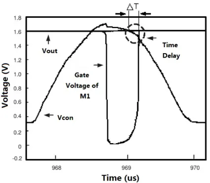
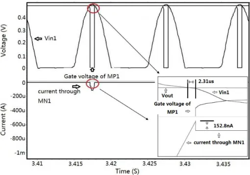
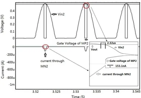
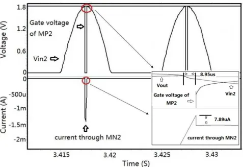
There will be reverse current fromVouttoVcon if the switch M1 is still on whenVout > Vcon. The reverse current has a big influence to the efficiency of the rectifier, and can reduce the power efficiency and voltage conversion efficiency severely.
As shown in Fig. 2.5, whenVcon decreases and gets smaller thanVout, the gate voltage of M1 does not change to high potential until a delay time△T. It means M1 is still on in the time interval △T and there will be reverse curent, for Vout > Vcon. In order to avoid the time delay△T, we set the transistor sizesW/LM12 > W/LM11, thus the current through the branch of M12 will be larger than that of M11 because of the current mirror. As in the saturation region, a largerIDmakes the overdrive voltage of M6 larger than M7, which
Figure 2.5: Output waveforms of the proposed rectifier with balanced transistor size under W/LM12 =W/LM11.
Figure 2.6: Simulated waveforms using current offset when|Vin |peak=1.7V.
Figure 2.7: Simulated waveforms using current offset when|Vin |peak= 0.7V.
makes an offset voltage Vo f f set in the comparator. Thus, the transistor switch turns off whenVout ≥ Vcon+Vo f f set, where theVo f f set is negative. This will compensate the△T and eliminate reverse current. WhenVoutchanges from 0.7 V to 1.8 V, the current through M11 and M12 will also increase which results in the value increasing of | Vo f f set |. Thus, we should adjust the ratio of W/LM12/W/LM11 to promise that there is no time delay with a 0.7V input.
Figures 2.6 and 2.7 show the performances under different input amplitudes. Addition- ally, taking into account the fabrication tolerances, we set the size ofW/LM12a little larger than the required value to compensate this influence. Comparing Figs. 2.6 and 2.7 with Fig. 2.5, the rectifier has even no time to delay. Then, there will be no reverse current in the whole cycle, which helps to reduce to output voltage ripple and maintain the high power efficiency.
Besides the reverse current, the operation voltage of the rectifier is also very important.
The minimum operation voltage of the comparator decides the minimum supply voltage
Table 2.1: Circuit transistor sizes.
Unite Size Multiply Factor Unite Size Multiply Factor
MP1 100µm/0.2µm 100 M5 40µm/0.5µm 50
MP2 100µm/0.2µm 100 M6 40µm/0.5µm 50
MN1 100µm/0.2µm 100 M7 40µm/0.5µm 50
MN2 100µm/0.2µm 100 M8 5µm/0.5µm 1
M1 100µm/0.2µm 50 M9 5µm/0.5µm 1
M2 100µm/0.2µm 50 M10 100µm/1µm 10
M3 100µm/0.2µm 50 M11 100µm/1µm 20
M4 40µm/0.5µm 50 M12 100µm/1µm 40
(input voltage peak amplitude) of our proposed rectifier, since the comparator is supplied by the output dc voltage. In order to promise the operation of comparator, the output voltage of the proposed rectifier must be larger than the minimum operation voltage of the comparator Thus, a small operation voltage comparator is necessary in this design.
As shown in Fig. 2.4 II, in each branch of the source-input stage, there is a pair of NMOS and PMOS transistors fromVoutorVcon to the ground. Consequently, the minimum operation voltage of the comparator is decided by the supply voltage of each branch and can be expressed as
Voutmin =max(|Vthp |+Vdsn+Vov,Vthn+ |Vdsp |), (2.2) where theVovis the over-dropout voltage of PMOS transistor. It means that the comparator can work well when both the voltages ofVconandVout are larger thanVoutmin, where|Vthp | is threshold voltage of PMOS and the dropout voltage of NMOS transistor is assumed to Vdsn. Since there is also |Vdsp |+Vdsn voltage drop through the first stage, the minimum input voltage of the rectifier can be expressed as
Vinmin = Voutmin+|Vdsp |+Vdsn, (2.3) where|Vdsp |is dropout voltage of PMOS transistor.
Figure 2.8: Test circuit for chip measurement.
2.4 Simulation and measurement results
The main aspects of the rectifier are minimum input voltageVinmin, output voltage efficiency, and the power efficiency, which will be discussed respectively.
The circuit has been simulated and fabricated with a standard 0.18µm CMOS process.
The circuit transistors size is shown in Table 2.1. A pure sinusoidal waveform whose frequency changes from 100 kHz to 1.5 MHz is applied to the input of the rectifier in the simulation. Additionally, a capacitance of 1µF and a load of 500 Ω are used. In the chip measurement, the transformer is used as the interface between input source and our proposed rectifier. Besides, the performance of the proposed rectifier under low frequency from 20 Hz to 100 Hz which is suited for vibration energy harvesting systems [13] is also simulated. The test circuit is shown in Fig. 2.8. As the input voltage of the rectifier is floating, inductive coupled coils are used to transfer the signal generated by the generator to rectifier. Probe1 and Probe2 can detect the input voltage amplitude. Probe1 and Probe3 are used to detect the voltage amplitude across the test resistor and calculate the input current. The ration of the coils is 1:1 with 16 turns. Inductance of the coil at 1.5 MHz is 812 µH. Figure 2.9 shows the micrograph of our proposed rectifier, the total chip area is 0.064mm2without the pads area.
Figure 2.9: Micrograph of the proposed rectifier.
Figure 2.10: Simulated output voltage under 100 kHz, 0.7 V input with RL=500Ω.
Figure 2.11: Simulated output voltage under 1.5 MHz, 0.7 V input with RL=500Ω.
2.4.1 Minimum input voltage and voltage conversion efficiency
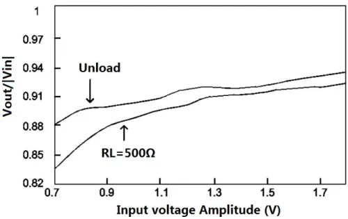
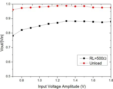
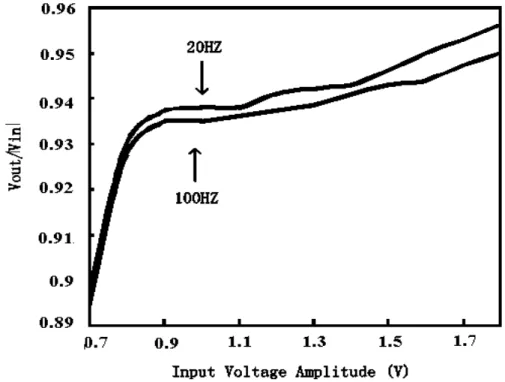
The minimum input voltage is very important especially for some low supply voltage systems. Figures 2.10 and 2.11 show the simulated output voltages. It indicates that the proposed rectifier can work at a minimum input voltage|Vin |of 0.7 V from 100 kHz to 1.5 MHz and provides a peak voltage conversion efficiencyVout/ |Vin |larger than 84%. The chip measurement results given in Fig. 2.12 and Fig. 2.13 also proved the proposed rectifier can work with a 0.7 V input peak amplitude. Figure 2.14 shows the peak voltage conversion efficiency versus different input amplitudes under a 1.5 MHz input. The performance in 100 kHz is shown in Fig. 2.15. Under both two frequencies, the peak voltage conversion rate is above 91% in average when| Vin |is from 0.7 V to 1.8 V. The chip measurement results of voltage conversion efficiency are given in Fig. 2.16 and Fig. 2.17. Figure 2.16 shows the voltage efficiency versus different loads, the performance of the unload condition is better than the performance with a load of 500 Ω, which is easy to be understood. The principle is the same as a voltage divider. Large load gets large output voltage. Figure 2.17 shows the voltage efficiency versus different input source frequency of 100 kHz and 1.5 MHz. The performance of 1.5 MHz is poor than 100 kHz due to faster switching of MOS transistors.
Figure 2.12: Measured output voltage under 100 kHz, 0.7 V input with RL=500Ω.
Figure 2.13: Measured output voltage under 1.5 MHz, 0.7 V input with RL=500Ω.
Figure 2.14: Simulated voltage conversion efficiency versus different input amplitudes with a 1.5 MHz input frequency.
Figure 2.15: Simulated voltage conversion efficiency versus different input amplitudes with a 100 kHz input frequency.
Figure 2.16: Measured peak voltage conversion efficiency versus different input amplitudes with a 100 kHz input frequency.
Figure 2.17: Measured peak voltage conversion efficiency versus different input amplitudes with a 500Ωload.
![Figure 1.7: Schematic of negative voltage converter with body bias block [25].](https://thumb-ap.123doks.com/thumbv2/123deta/9853065.1898348/27.918.181.804.119.491/figure-schematic-negative-voltage-converter-body-bias-block.webp)
![Figure 1.11: Rectifier for UHF application based on negative voltage convertor [28].](https://thumb-ap.123doks.com/thumbv2/123deta/9853065.1898348/31.918.253.718.108.455/figure-rectifier-uhf-application-based-negative-voltage-convertor.webp)