andShinji MIYANO ,Senior Member
SUMMARY The self-improvement of static random access memory (SRAM) cell stability by post-fabrication high-voltage stress is experimen- tally demonstrated and its mechanism is analyzed using 4k device-matrix- array (DMA) SRAM test element group (TEG). It is shown that the stabil- ity of unbalance cells is automatically improved by merely applying stress voltage to the VDDterminal of SRAM. It is newly found that|VTH|of the OFF-state pFETs in the SRAM cell is selectively lowered which improves the cell stability and contributes to the self-improvement.
key words: transistor, MOSFET, variability, off-state stress
1. Introduction
The size of metal-oxide-semiconductor field effect transis- tors (MOSFETs) in large scale integrated circuits (VLSI) has been rapidly scaled down for more than forty years for higher performance, lower power consumption, and higher integration. As the transistors are miniaturized, the random variability of transistor characteristics has become more ob- vious [1]–[3]: each transistor has different threshold voltage (VTH) and drain current even though the transistor dimen- sion is the same, leading to severe reduction of circuit op- eration margin and yield loss in VLSI. It is well known that the random variability is caused by the statistical nature of dopant atoms in the transistor channel which is called ran- dom dopant fluctuation (RDF) [4]–[13]. The number and position of impurity atoms in the channel depletion layer, that determine VTHof the transistor, is randomly distributed.
The increase in random variability in scaled MOSFETs is one of the most serious obstacles for further device scaling and supply voltage (VDD) lowering.
Static random access memory (SRAM) is a high-speed, low power memory and is widely used as a cache mem- ory in logic VLSIs including microprocessors and micro- controllers. An SRAM cell is typically composed of six transistors (6T). The 6T SRAM cell has two cross-coupled complementary MOS (CMOS) inverters and two pass gate transistors. It is also well known that the stability of 6T SRAM cells is largely affected by the random variability of transistor characteristics [14]–[19]. A SRAM cell that hap- pens to include extremely high VTHor low VTHtransistors is unbalanced. Some of such unbalanced cells are likely to
Manuscript received February 5, 2013.
†The authors are with Institute of Industrial Science, The Uni- versity of Tokyo, Tokyo, 153-8505 Japan.
††The author is with The Semiconductor Technology Academic Research Center (STARC), Yokohama-shi, 222-0033 Japan.
a) E-mail: [email protected] DOI: 10.1587/transele.E96.C.759
fail, in particular at low VDD, which leads to a severe yield loss of SRAM. The stability in the read operation is deter- mined by the balance of six transistors, while the stability in the retention operation is determined by the balance of four transistors that compose the two CMOS inverters.
It is more difficult to reduce VDDof SRAM due to this variability issue than VDDof logic circuits. Various circuit techniques and new cell structures have been proposed, in- cluding a 8-transistor SRAM cell [17] and a 10-transistor SRAM cell [18], to improve the cell stability and reduce the minimum operation voltage (Vmin) of SRAM. However, these techniques suffer from severe area penalty or speed loss. Therefore, it is essential to develop a new technique to improve the SRAM cell stability even in the existence of transistor variability and reduce Vmin of logic VLSI for ultra-low power and ultra-low voltage applications.
Recently, we have proposed a new concept of a post- fabrication technique to improve the stability of SRAM cells automatically by simply applying stress voltage to the VDD
terminal of SRAM cell array [20], [21]. This technique can apply to the stability self-improvement in both the read op- eration [20], [21] and the retention operation [22]. When ap- plied to the retention self-improvement, the stronger nFET and pFET out of four transistors in the two inverters are se- lectively stressed and their|VTH|is raised (and hence these transistors are weakened), while the weaker nFET and pFET are not stressed, resulting in automatic self-improvement of the cell stability.
In this paper, the post fabrication self-improvement in the retention stability is experimentally demonstrated using 4k SRAM device matrix array (DMA) test element group (TEG). VTH of all transistors in 4k cells before and after stress are measured and the self-improvement mechanisms are investigated by analyzing these data. It is newly found that not only|VTH|of the stronger pFET in the cell is raised, but also|VTH|of the weaker pFET in the cell is selectively lowered, resulting in very effective self-improvement phe- nomena.
2. Self-Improvement Technique
Figure 1 shows a schematic of 6T SRAM cell. The two stor- age nodes in the cell are named as VL and VR. The left and right nFETs and the left and right pFETs that compose two CMOS inverters are named as TnL, TnR, TpL, and TpR, respectively. In the self-improvement technique, the stress Copyright c2013 The Institute of Electronics, Information and Communication Engineers
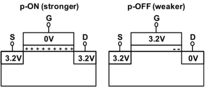
Fig. 1 A schematic of 6T-SRAM cell. The two storage nodes are named as VL and VR. In this example, it is assumed VL is low and VR is high.
The left pFET is “p-OFF” and the right pFET is “p-ON”.
voltage is applied to the VDD terminal of SRAM cell ar- ray. VDDis raised from 0 V to the stress voltage (3.2 V in this study), keeping the word line (WL) at 0 V. The scan time (stress time) is only several seconds. Since the VTH shift of nFETs was small enough while the |VTH| shift of pFETs is much larger by the stress voltage of 3.2 V, the self-improvement technique in the retention operation is ex- plained based on the pFET|VTH|shift in the following.
The SRAM cell is bi-stable in the retention condition when VDD is high enough and can store one bit per cell.
The storage node VR can be either “high” or “low” in the bi-stable operation. However, when VDD is very low (for example, 0.1 V), each SRAM cell is not bi-stable because of the unbalance of four transistors that compose two inverters caused by the VTH variability. Then, VR is fixed to only
“high” in some cells at very low VDDand VR is fixed to only
“low” in the other cells. In this technique, VDDis scanned from 0 V to 3.2 V, and VR is fixed to “high” or “low” at the beginning of the scan.
Here, the reason for fixed “high” or “low” in VR at low VDD is discussed in more detail. Let us assume that VR is fixed to “high” at very low VDD in a certain cell as shown in Fig. 1. This means that the strength to pull up VR is stronger than the strength to pull up VL. Therefore, TpR or TnL may be stronger (lower|VTH|) than TpL or TnR.
Here, we call a pFET connected to the high node as “p- ON” and a pFET connected to the low node as “p-OFF”, because the former is at the ON-state and the latter is at the OFF-state. Similarly, “n-ON” and “n-OFF” are defined. It should be noted that, if p-ON is weakened, the cell stabil- ity is certainly improved because the strength to pull up VR is weakened. Therefore, it is stated in the following that p- ON is the stronger pFET (that should be weakened for cell stability improvement) and p-OFF is the weaker pFET (that should be strengthened).
Next, let us consider the situation where VDDis raised to 3.2 V. The negative gate bias is automatically applied to only p-ON that is stronger because this transistor is at the
ON-state. This bias condition is just the same as that of neg- ative bias temperature instability (NBTI) stress, as shown in Fig. 2(a). The positively charged interface traps are gen- erated. Then, |VTH| of p-ON is selectively raised and this transistor is weakened. On the other hand, the bias condi- tion of p-OFF which is weaker is shown in Fig. 2(b). The gate voltage is the same as the source voltage, and the NBTI stress is not applied to p-OFF. As a result, the cell stability is improved [20]–[22].
3. Experimental Results
3.1 Stress and Measurement Conditions
6T SRAM DMA TEG [21], [23], [24] was fabricated by the 40 nm planar bulk technology. In this SRAM DMA TEG, terminals for VDD, WL, two BLs, VL, and VR can be ac- cessed. Hence, characteristics of all 6 transistors as well as static noise margin (SNM) and retention noise margin (RetNM) [19] in each cell can be directly measured.
In order to determine at what temperature the high stress voltage should be applied, the temperature depen- dence of RetNM was measured. Figure 3 shows measured correlation between RetNM of 4k SRAM cells at 25◦C and 100◦C. It is found that the correlation is not good. This result indicates that stable cells at 25◦C are not necessar- ily stable at 100◦C. Since the cell unbalance is more se- vere at higher temperature, the high voltage stress for self- improvement should be applied at higher temperature. In this study, the high voltage stress to VDD was applied at 100◦C.
3.2 Measured|VTH|Shift by High Voltage Stress
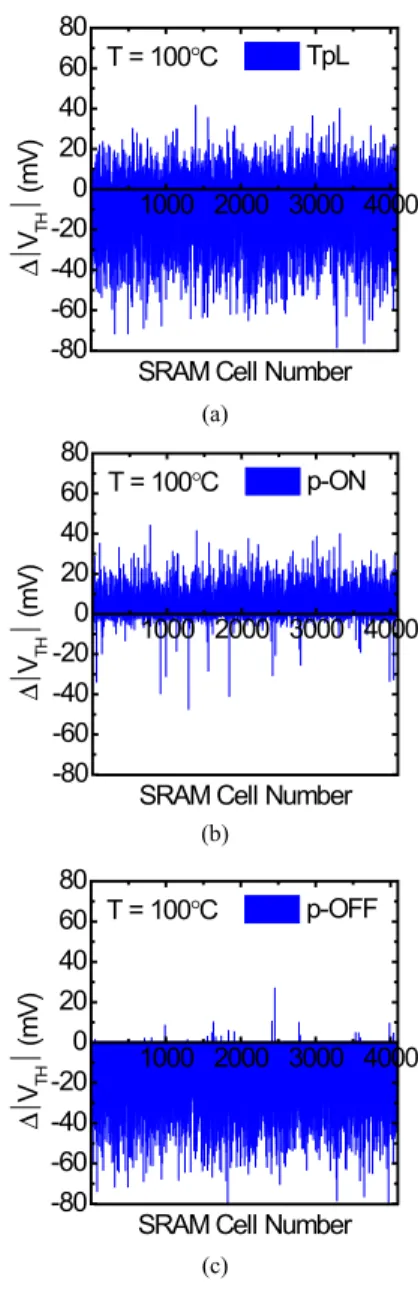
First, we pay attention to the|VTH|shift by the high voltage stress in the left pFET (TpL) measured at 100◦C. Figure 4(a) shows measured|VTH|shift of TpL of 4k SRAM cells by the stress voltage of 3.2 V. The horizontal axis is the cell number. The shift is random: some cells show positive shift while some show negative shift. Since whether VL is fixed to “high” or “low” at low VDDis random, this result is quite reasonable.
Next, we pay attention to the|VTH|shift of p-ON and p- OFF. By checking “high” or “low” of VL and VR, it is easy
Fig. 3 Correlation between measured RetNM of 4k SRAM cells at 25◦C and 100◦C.
to determine which pFET is p-ON or p-OFF. The|VTH|shift data of p-ON and p-OFF are extracted from data of all left pFET (TpL) and right pFET (TpR). Figure 4(b) shows mea- sured|VTH|shift of p-ON which was originally stronger and should be weakened for the self-improvement. It is found that majority of p-ON transistors show positive|VTH|shift, indicating that p-ON is weakened and the self-improvement mechanism works. This positive|VTH|shift is caused by the NBTI stress.
Figure 4(c) shows measured |VTH| shift of p-OFF which is weaker. It is newly found that almost all p-OFF transistors show negative|VTH|shift, indicating that p-OFF which was originally weak is strengthened by the high volt- age stress, which is favorable for the self-improvement. The shift is even larger than that of p-ON. The p-OFF transis- tors are in the OFF-state: gate is high, source is high, and drain is low. Therefore, the gate bias is zero with respect to the source voltage, but the gate bias is positive with respect to the drain voltage. The stress caused by this bias condi- tion is often called the OFF-state stress [25], [26]. Negative charges are injected into gate dielectric near drain and neg- ative|VTH|shift (positive VTHshift) is observed.
Figures 4(b) and (c) show that not all cells exhibit the favorable|VTH|shift, i.e. some cells exhibit negative|VTH| shift of p-ON and positive|VTH| shift of p-OFF, which is the opposite direction to the self-improvement. To investi- gate the behaviors of|VTH|shifts in more detail, the corre- lation between|VTH|shift (Δ|VTH|) of p-ON andΔ|VTH|of p-OFF is plotted as shown in Fig. 5. If the plots are located in the fourth quadrant (positiveΔ|VTH|of p-ON and negative Δ|VTH|of p-OFF), the shifts are favorable. It is found that a cluster of cells are plotted in the fourth quadrant in clus- ter as expected, although some cells are spread out to the third quadrant. However, it is also found that some cells (de- noted in the solid symbols in Fig. 5) are located in the second quadrant, which may result in the degradation of cell stabil- ity. The reason for this unfavorable behavior is discussed later.
Fig. 4 Measured|VTH|shift at 100◦C of (a) 4k TpL transistors, (b) 4k p-ON transistors, and (c) 4k p-OFF transistors by applying VDDstress of 3.2 V at 100◦C.
3.3 Measured Butterfly Curve Change by Stress
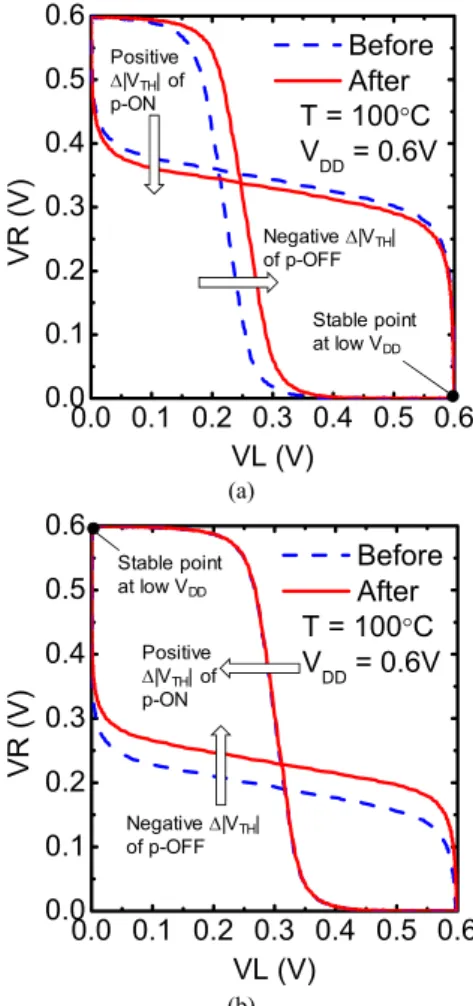
Figure 6 shows examples of measured butterfly curves in the retention condition (WL is 0 V) before and after applying high voltage stress. Here, RetNM(L) is defined as the square of the left eye of the butterfly curve and RetNM(R) is the square of the right eye. RetNM is the smaller square of two eyes of the butterfly curve. The change of butterfly curves by the stress is explained in the following.
As mentioned in Sect. 2, VR is fixed to “low” or “high”
at the beginning of the VDDscan. In a cell in Fig. 6(a), “VR
=low” is stable at low VDD, and hence RetNM(R) is larger and RetNM(L) is smaller. The right pFET (TpR) is the p- OFF. When high voltage stress is applied,|VTH|of p-OFF is lowered, and the inverter curve by TpR and TnR moves to
Fig. 5 Correlation between measured|VTH|shift of p-OFF and measured
|VTH|shift of p-OFF by high voltage stress. Cells that show the opposite
|VTH|shifts are denoted by solid symbols.
Fig. 6 Examples of measured butterfly curves in the retention condition before and after high voltage stress. (a) A cell where “VR=low” is stable at very low VDD. (b) A cell where “VR=high” is stable at very low VDD.
the right direction, as shown in Fig. 6(a). Similarly, raised
|VTH| of p-ON moves the inverter curve by TpL and TnL down. In this way, both p-ON and p-OFF contribute to en- large RetNM(L), resulting in the cell stability improvement.
Fig. 7 Measured RetNM distribution of 4k cells before and after the high voltage stress to VDDat 100◦C.
In a cell in Fig. 6(b), on the other hand, “VR=high” is stable, and hence RetNM(R) is smaller. In this specific cell, only negative Δ|VTH| of p-OFF contributes but no Δ|VTH| of p-ON is observed. The cell stability of this cell is also improved because RetNM(R) is enlarged.
3.4 Retention Noise Margin Improvement
Figure 7 shows measured RetNM distributions before and after the high voltage stress to VDD in 4k SRAM cells.
Clear improvement of RetNM is observed, particularly in the worst cell that have originally the smallest RetNM. Since Vminis determined by the worst cell, this self-improvement technique largely contributes to the yield enhancement of SRAM cells.
3.5 Analysis of|VTH|Distributions
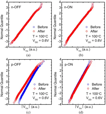
Here, we get back to the discussions of|VTH|distributions in cell transistors. Figure 8 shows|VTH|distributions of n- ON, n-OFF, p-ON, and p-OFF before and after high voltage stress. n-ON and n-OFF show almost no VTHshift by high voltage stress of 3.2 V, as mentioned in Sect. 2. A slight
|VTH|increase and no variability degradation are observed in p-ON. However, it should be noted that not only large
|VTH|decrease but also variability degradation is clear ob- served in p-OFF as shown in Fig. 8(d). It is indicated that, in this self-improvement technique, SRAM cell stability is improved but the transistor variability is degraded.
This phenomenon is well explained by the variability of pair-matched transistors. Figure 9 shows the measured dis- tribution of the|VTH|difference in the left and right pFETs (TpL and TpR) in 4k SRAM cells. The|VTH|matching of two pFETs in a cell is greatly improved. The cell stability is basically determined by the matching of transistors. By the high voltage stress, the stronger pFETs are weakened and the weaker pFETs are strengthened, resulting in improved matching of pFETs. This mechanism contributes to the self- improvement of SRAM cell stability.
Fig. 8 Measured|VTH|distributions before and after high voltage stress in (a) n-ON, (b) n-OFF, (c) p-ON, and (d) p-OFF. No VTHchange was observed by stress in nFETs. It should be noted that|VTH|variability is degraded in p-OFF.
Fig. 9 Measured distribution of|VTH|difference in TpL and TpR before and after high voltage stress.
3.6 Analysis of RetNM Improvement
Figure 10 shows correlation between RetNM improvement and initial RetNM before stress. Apparently, negative cor- relation is observed, indicating that more unbalance cells, which originally have small RetNM, are saved. Clear im- provement of RetNM is observed in worst cells, and Vminis apparently improved. RetNM of some cells that have origi- nally large RetNM is degraded as shown in the figure.
Figure 11 shows measured correlation between RetNM before stress and RetNM after stress. Similarly to Fig. 8, the stability of SRAM cells that were originally unstable are
Fig. 10 Correlation between measured RetNM change by stress at 100◦C and the initial RetNM before stress in 4k cells.
Fig. 11 Correlation between measured RetNM after stress and measured RetNM before stress. The cells that show the opposite|VTH|shifts in Fig. 5 are denoted by solid symbols.
saved. Originally stable cells that have large RetNM before stress still have sufficient large RetNM after stress. There- fore, although the stability of some stable cells is degraded by the high voltage stress, this phenomenon does not result in yield loss of SRAM.
In Fig. 11, the cells that show the opposite|VTH|shift in Fig. 5 are denoted in the solid symbols. It is found that all the cells that were originally unstable (small RetNM be- fore stress) are favorably shifted by the high voltage stress, and cells that show the opposite |VTH| shift are originally stable cells. It is considered that these cells are so stable that “high” or “low” of the storage nodes is not determined at the beginning of VDD scan. As a result, p-ON and p- OFF are interchanged resulting in the opposite|VTH|shift.
Anyway, this phenomenon does not result in yield loss of SRAM, either.
4. Conclusions
A new concept of post-fabrication self-improvement tech- nique of SRAM cell stability is experimentally demon- strated in 4k SRAM cells. It is newly found that, not only the stronger pFET in a cell is weakened, but also the weaker pFET is strengthened by the OFF-state stress due to high voltage stress, which contributes to the self-improvement of SRAM cell stability. This post-fabrication technique will be essential in improving degraded yield of future large-scale SRAM with increased transistor variability.
Acknowledgments
This work was carried out as a part of the Extremely Low Power (ELP) project supported by METI and NEDO. The authors would like to thank Prof. Takayasu Sakurai for his continuous encouragements.
References
[1] B. Hoeneisen and C.A. Mead, “Fundamental limitations in mi- croelectronics — I. MOS technology,” Solid-State Electron., vol.15, pp.819–829, 1972.
[2] R.W. Keyes, “The effect of randomness in the distribution of im- purity atoms on FET thresholds,” Appl. Phys., vol.8, pp.251–259, 1975.
[3] M.J.M. Pelgrom, A.C. Duinmaijer, and A.P.G. Welbers, “Matching properties of MOS transistors,” IEEE J. Solid-State Circuits, vol.20, no.5, pp.1433–1439, May 1989.
[4] T. Mizuno, J. Okamura, and A. Toriumi, “Experimental study of threshold voltage fluctuation due to statistical variation of channel dopant number in MOSFET’s,” IEEE Trans. Electron Devices, vol.1, no.11, pp.2216–2221, Nov. 1994.
[5] A. Asenov, “Random dopant induced threshold voltage lowering and fluctuations in sub-0.1µMOSFET’s: A 3-D ‘atomistic’ simulation study,” IEEE Trans. Electron Devices, vol.45, no.12, pp.2505–2513, Dec. 1998.
[6] Y. Yasuda, M. Takamiya, and T. Hiramoto, “Separation of effects of statistical impurity number fluctuations and position distribution on Vth fluctuations in scaled MOSFETs,” IEEE Trans. Electron De- vices, vol.47, no.10, pp.1838–1842, Oct. 2000.
[7] K.J. Kuhn, “Reducing variation in advanced logic technologies: Ap- proaches to process and design for manufacturability of nanoscale CMOS,” IEDM Tech Dig., pp.471–474, 2007.
[8] K. Takeuchi, T. Fukai, T. Tsunomura, A.T. Putra, A. Nishida, S. Kamohara, and T. Hiramoto, “Understanding random threshold
Mogami, “Analysis and prospect of local variability of drain current in scaled MOSFETs by a new decomposition method,” VLSI Symp.
Tech. Dig., pp.97–98, 2010.
[13] T. Tsunomura, A. Kumar, T. Mizutani, A. Nishida, K. Takeuchi, S. Inaba, S. Kamohara, K. Terada, T. Hiramoto, and T. Mogami,
“Investigation of threshold voltage variability at high temperature using Takeuchi plot,” Appl. Phys. Express, vol.3, no.11, 114201, Nov. 2010.
[14] A.J. Bhavnagarwala, X. Tang, and J.D. Meindl, “The impact of in- trinsic device fluctuations on CMOS SRAM cell stability,” IEEE J.
Solid-State Circuits, vol.36, no.4, pp.658–665, April 2001.
[15] F. Tachibana and T. Hiramoto, “Re-examination of impact of intrin- sic dopant fluctuations on static RAM (SRAM) static noise margin,”
Jpn. J. Appl. Phys., vol.44, no.4B, pp.2147–2151, April 2005.
[16] L. Chang, D.M. Fried, J. Hergenrother, J.W. Sleight, R.H. Dennard, R.K. Montoye, L. Sekaric, S.J. McNab, A.W. Topol, C.D. Adams, K.W. Guarini, and W. Haensch, “Stable SRAM cell design for the 32 nm node and beyond,” VLSI Symp. Tech. Dig., pp.128–129, 2005.
[17] N. Verma and A. Chandrakasan, “A 65 nm 8T Sub-Vt SRAM em- ploying sense-amplifier redundancy,” ISSCC Tech. Dig., pp.328–
329, 2006.
[18] B.H. Calhoun and A. Chandrakasan, “A 256 KB sub-threshold SRAM in 65 nm CMOS,” ISSCC Tech. Dig., pp.628–629, 2006.
[19] A. Bhavanagarwala, S. Kosonocky, C. Radens, K. Stawiasz, R.
Mann, Q. Ye, and K. Chin, “Fluctuation limits & scaling opportuni- ties for CMOS SRAM cells,” Proc. IEDM, pp.675–678, 2005.
[20] M. Suzuki, T. Saraya, K. Shimizu, T. Sakurai, and T. Hiramoto
“Post-fabrication self-convergence scheme for suppressing variabil- ity in SRAM cells and logic transistors,” VLSI Symp. Tech. Dig., pp.148–149, 2009.
[21] M. Suzuki, T. Saraya, K. Shimizu, A. Nishida, S. Kamohara, K.
Takeuchi, S. Miyano, T. Sakurai, and T. Hiramoto, “Direct mea- surements, analysis, and post fabrication improvement of noise mar- gins in SRAM cells utilizing DMA SRAM TEG,” VLSI Symp. Tech.
Dig., pp.191–192, 2010.
[22] M. Suzuki, T. Saraya, K. Shimizu, T. Sakurai, and T. Hiramoto, “Im- provement of static noise margin in SRAM by post-fabrication self- convergence technique,” Int. Semiconductor Device Research Sym- posium (ISDRS), TP7-03, 2009.
[23] X. Song, M. Suzuki, T. Saraya, A. Nishida, T. Tsunomura, S. Kamo- hara, K. Takeuchi, S. Inaba, T. Mogami, and T. Hiramoto, “Impact of DIBL variability on SRAM static noise margin analyzed by DMA SRAM TEG,” IEDM Tech. Dig., pp.62–65, 2010.
[24] T. Hiramoto, M. Suzuki, X. Song, K. Shimizu, T. Saraya, A. Nishida, T. Tsunomura, S. Kamohara, K. Takeuchi, and T. Mogami, “Direct measurement of correlation between SRAM noise margin and indi- vidual cell transistor variability by using device matrix array,” IEEE Trans. Electron Devices, vol.58, no.8, pp.2249–2256, Aug. 2011.
[25] C. Yang, Z. Wang, C. Tan, and M. Xu, “The degradation of p-MOSFETs under off-state stress,” Microelectronics J., vol.32,
Toshiro Hiramoto received the B.S., M.S., and Ph.D. degrees in Electronic Engineering from University of Tokyo in 1984, 1986, and 1989, respectively. In 1989, he joined Device Development Center, Hitachi Ltd., Ome, Japan, where he was engaged in the device and circuit design of ultra-fast BiCMOS SRAMs. In 1994, he joined Institute of Industrial Science, Univer- sity of Tokyo, Japan and has been a Professor since 2002. His research interests include low power CMOS devices design, variability, silicon nanowire transistors, and silicon single electron transistors. Dr. Hiramoto is a Fellow of Japan Society of Applied Physics, and is a member of IEEE. He was on the Committee of International Electron Devices Meeting (IEDM) in 2003–2009. He has served on the Program Committee of Symposium on VLSI Technology since 2001, and he is the Program Chair in 2013.
Anil Kumar received the B.Sc. and M.Sc.
degrees in Physics from the Meerut University in 1993, and 1995. He received the Ph.D. de- gree in Microelectronics from the Delhi Uni- versity in 2001. He worked as a Post Doctoral Researcher in University of Tokyo from 2002–
2004. He joined FD SOI CMOS Device Devel- opment Center, OKI Electric Ind. Co. Ltd., To- kyo, Japan in 2004, where he was engaged in the device development for ultra low power applica- tions. In 2009, he joined Institute of Industrial Science, University of Tokyo, Japan, as a Specialist Researcher. His re- search interests include low power CMOS devices design, variability in scaled transistors and SRAM. Dr. Anil Kumar is a member of IEEE and JSAP.
Takuya Saraya received the B.S. and M.S. degrees in electronic engineering from Chiba University in 1993 and 1995, respec- tively. In 1995, he joined Institute of Industrial Science, University of Tokyo. His research in- terests include fabrication and characterization of nanoscale CMOS transistors.
search Center. His current research interests in- clude ultra-low-power SRAM, DRAM, and sys- tem LSIs. He has served as a Program Committee Member for IEEE Cus- tom Integrated Circuits Conference (CICC) and as a Guest Associate Editor of IEICE Transactions on Electronics.