SUMMARY We have investigated the microwave-detected photocon- ductivity responses from the amorphous In–Ga–Zn–O (a-IGZO) thin films.
The time constant extracted by the slope of the slow part of the reflectivity signals are correlated with TFT performances. We have evaluated the in- fluences of the sputtering conditions on the quality of a-IGZO thin film, as well as the influences of gate insulation films and annealing conditions, by comparing the TFT characteristics with the microwave photoconductivity decay (µ-PCD). It is concluded that theµ-PCD is a promising method for in-line process monitoring for the IGZO-TFTs fabrication.
key words: oxide semiconductor, thin film transistor, microwave-detected photoconductivity decay, in-line process monitoring
1. Introduction
Amorphous In–Ga–Zn–O (a-IGZO) is a promising mate- rial for highly efficient thin-film-transistors (TFTs) in next generation flat panel display since one can obtain higher field effect mobilities over 10 cm2/Vs with a maturated film formation technique [1]. It is widely recognized that the performances of a-IGZO TFTs are governed by the elec- tronic properties of the films, which are often modified by their manufacturing process. As compared with conven- tional channel materials such as amorphous Si, the a-IGZO is extremely sensitive to the manufacturing process of the TFTs, thus, stabilization of the film characteristics is an is- sue which should be solved to realize the a-IGZO TFTs for practical use.
It has been difficult to presume the performances of the TFTs only from the characteristics of the a-IGZO thin films.
In our previous study, it was found that a strong correlation between the TFT mobilities and the peak values of the mi- crowave photoconductivity decay (µ-PCD) signals for the corresponding a-IGZO thin films [2]–[3]. The decay curve of theµ-PCD consists of at least two kinds of decay compo- nents, namely the fast and the slow decay curves. The ori- gin of the latter is attributed to reemission of the electrons captured at the defect-like states just below the conduction band minimum (CBM). Therefore, analyzing the slow decay
Manuscript received February 28, 2014.
Manuscript revised June 9, 2014.
†The authors are with Kobe Steel Ltd., Kobe-shi, Hyogo, 651- 2271 Japan.
††The author is with Kobelco Research Institute Inc., Kobe-shi, Hyogo, 651-2271 Japan.
a) E-mail: [email protected] DOI: 10.1587/transele.E97.C.1055
curves obtained by theµ-PCD measurements could be use- ful tool for monitoring the change of the electronic proper- ties during the fabrication process to manage the IGZO-TFT performances.
According to several researchers [4]–[9], the reliability of the IGZO-TFTs is related to defect states below the CBM in the a-IGZO thin films. In particular, during the light- illumination and negative-bias temperature stress (LNBTS), it is considered that the defect-like states are formed, which causes the change of the threshold voltage (Vth) of the TFTs.
In the preset study, we made detailed investigation on the slow decay component in the µ-PCD signals from the a-IGZO thin films and correlated with the Vthshift induced during the LNBTS test. We have proposed a practical eval- uation parameter “τ2” which can be used as an in-line mon- itoring tool for the a-IGZO TFT fabrication processes.
2. Interpretation ofµ-PCD Signals and Determination ofτ2as an Evaluation Parameter for LNBTS Generally, in the photoconductivity responses from semi- conductors having a decay constant ofτ, the density of ex- cess carriers after photoexcitation can be described by the following equation;
n(t)=n0exp(−t/τ), (1) wheren0is the carrier density just after the photoexcitation;
tis the time after the photoexcitation.
Figure 1 shows a typical µ-PCD decay curve of the a-IGZO thin film. The decay curve can be divided into three components; the peak value, and the two kinds of de- cay including the fast and the slow decay constants, which is different from the decay curves obtained on LTPS thin films [10]. According to our previous study [3], we assumed that the density of the carriers participating in the microwave conductivity obeys the following equation after photoexci- tation:
n(t)=n0{exp(−t/τf)+exp[−(t/τs)β], (2) where areτf andτsare the fast decay and the slow decay time constants, respectively; and βis the stretching expo- nent. The slow decay was found to be related to the reemis- sion and recombination of trapped carriers from the defect Copyright c⃝2014 The Institute of Electronics, Information and Communication Engineers
Fig. 1 The ideal signal and decay curve of microwave photoconductivity decay (µ-PCD) method.
states located at 0.1∼0.2 eV. The fact that the slow decay can be described by a stretch exponential [11]–[13] suggests that the energy level of the defect states is broad and close to the Fermi level of the system.
As described in the previous section, one of the origins of the Vth shift of the IGZO-TFTs during the LNBTS test is the change of the defect-like states just below the CBM in the a-IGZO thin films. This issue is examined by some researchers using a simulation model [14], i.e., the influ- ences of the energy levels of the defectsEGDwere evalu- ated by using the model where the donor-like defect-related states were put below the CBM near the back channel of the TFTs. These simulation results indicated that the TFT properties were affected by the localized states, which were observed in the TFT transfer curves by the variation of the hump shoulder depending on theEGD. When the donor-like defect states are located above the Fermi level, the defect- like states are instantly ionized, which results in the hump phenomena in the TFT transfer curves. In the case that the donor-like defects form very shallow states below the CBM, the TFT transfer curves show a parallel shift during the LNBTS tests. On the other hand, the hump phenomena are frequently observed during the LNBTS. The formation of the hump implies that the values of theEGDare rather deep compared from the defect levels mentioned above. This is the case in the present study. Therefore, we have investi- gated the slow decay constant ofµsec order range not less thanµsec. The slow decayτ2corresponds to the slope be- tween t1and t2, as shown in Fig. 1. The value ofτ2is calcu- lated from the slope of the decay curves in the region where the almost exponential decrease is observed and on the order of a few microseconds.
As a result, the following equation is considered:
n(t)=n0exp(−t/τ1)+n1exp[−(t/τ2)], (3) The βvalue describes the relaxation of the system to equilibrium [15]–[17]. β=1 is substituted since the slow decay in theµsec range shows good linearity in the semi- log plots.
Fig. 2 The principal ofµ-PCD method.
3. Experimental
3.1 Apparatus ofµ-PCD
The µ-PCD method is a non-destructive, contactless tech- nique that enables characterization of the capture, recom- bination, and relaxation of laser-excited carriers by observ- ing the temporal response of the microwave reflectivity [10].
The apparatus ofµ-PCD system is shown in Fig. 2. The ex- cess carriers are injected into the films by the laser pulse.
The change in the carrier concentration after the excitation is observed by the microwave reflectivity.
In general, the evaluation of thin films is difficult to secure enoughS/Nratio for signal detection since the thick- ness of the film is very thin like 40 nm and the quality of the film is not as good as that for crystal. To overcome this problem, the differential detection system shown in Fig. 2 is utilized. Two waveguides are equipped with and only the film under the signal waveguide is illuminated. Output from reference waveguide contains noise, while that from signal waveguide contains both signal and noise. By subtracting the both output, we can extract onlyµ-PCD signal. This dif- ferential detection system improves theS/Nratio more than 500 times.
3.2 Sample Preparation
The schematics of the a-IGZO films for µ-PCD measure- ments were shown in Fig. 3(a). The a-IGZO films were deposited on glass substrates by DC sputtering using an InGaZnO4 target. The thickness of the films is fixed at 40 nm. The film is then annealed at 350◦C for 1 h in air.
The duration of the annealing was fixed at 60 min otherwise mentioned.
For evaluation of the influence of hydrogen contents in gate insulators (GIs), the following samples were prepared.
The schematics of the samples are shown in Fig. 3(b). The 250 nm CVD-SiOx layer was deposited on glas substrates.
The a-IGZO films were deposited on the glass substrates covered with the SiOxlayer by DC sputtering with the same conditions mentioned above. The thickness of the film was
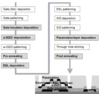
Fig. 3 The cross-sectional structures of (a) a-IGZO film forµ-PCD mea- surement, (b) a-IGZO film for evaluating influence of a gate insulator (GI) and (c) a-IGZO TFT.
fixed at 40 nm, and then the films were also annealed in air.
Figure 3(c) schematically shows a cross-sectional structure of the a-IGZO TFTs with a bottom gate struc- ture. The fabrication process of the TFTs is as follows: The 250 nm CVD-SiOx layer was used as a GI, which was de- posited on a glass substrate with a Mo gate electrode. A- IGZO films with a thickness of 40 nm were deposited on the substrates. The a-IGZO films were photolithographi- cally pattered and the samples were annealed at 350◦C for 1 h in air. Then, the source and drain electrodes consisting of Mo were deposited and patterned. The CVD-SiN layer was continuously formed as a passivation layer after depo- sition of CVD-SiOx layer. Finally, the a-IGZO TFTs were annealed at 250◦C for 1 h in N2.
The channel length (L) of the TFT is 20µm, while the channel width (W) is 210µm. The measurements of the transfer curves and the values of the Vthshift (∆Vth) during the LNBTS tests were performed by using a semiconductor parameter analyzer (Keithley 4200-SCS).
The gate voltage (Vgs) was swept between −30 and 30 V while the drain voltage (Vds) is fixed at 10 V. The Vth
is defined as Vds when the value of Ids exceeds 1nA. The LNBTS test is carried out under the following conditions:
Vgs and Vds are fixed at−20 and 10 V, respectively, and a substrate temperature is set at 60◦C. The luminance during the LNBTS test is 25,000 cd/m2 (nit). In the LNBTS test, the∆Vthis defined as;∆Vth=Vth,7200s– Vth,initial, where Vth,7200sis the Vthvalue after 7200 sec and Vth,initialis the initial Vth.
4. Results
The values of the Vthshift and theτ2are plotted in Fig. 4 as a function of oxygen partial pressure during the a-IGZO depo- sition. This graph shows excellent correlation between the τ2estimated from the slow decay and the valued of the Vth
shift under the LNBTS test, the latter of which is strongly influenced by the parameters of sputtering conditions. The Vth shift becomes smaller with increasing the partial pres-
Fig. 4 Vthshift by LNBTS andτ2values in terms of oxygen partial pressure.
Fig. 5 Decay curves inµ-PCD in terms of annealing time at 350◦C in air.
sure of oxygen during the deposition of the a-IGZO. When the partial pressure of oxygen is 10% and more, the value of the Vthshift is saturated, and the value of Vthshift becomes less than 1 V. With decreasing the oxygen partial pressure during the a-IGZO sputtering, the carrier concentration in the films increases due to an increase of the donor-like de- fect [18]. Therefore, it is reasonable thought that the value of τ2 has correlation in the oxygen partial pressure. The good correlation between the∆Vthand theτ2value suggests that the donor-like defects introduced in the films affect the TFT stability. Deduced from the result of Fig. 4, the most desirable sputtering conditions for acquiring the best stabil- ity with our sputtering apparatus could be at around 10%
oxygen addition.
Secondly, the effects of annealing were evaluated. Fig- ure 5 shows theµ-PCD decay curves from the a-IGZO thin films with various annealing duration. In the experiments, the annealing temperature was fixed at 350◦C (in air) and the annealing time was varied between 5 and 120 min. After annealing at least 5 min, the decay curves were drastically changed compared with that obtained before annealing. Af-
Fig. 6 Vthshift by LNBTS andτ2values in terms of annealing time at 350◦C in air.
Fig. 7 Relationship between Vthshift by LNBTS andτ2values.
ter annealing for 30 min, the slow decay curve is slightly moved downward, and then that of 60 min did the same way.
The slow decay curve of 120 min annealing sample was al- most the same as that for 60 min.
The values of the Vthshift and theτ2are summarized in Fig. 6. Both the∆Vth and theτ2after 60 min-annealing become the smallest than the others, therefore the anneal- ing at 60 min could be the best conditions. After annealing at 120 min, the Vthshift and theτ2 values were slightly in- creased. This result should be attributed to the formation of two kinds of defect states during the annealing. It has been reported that the desorption of oxygen and zinc from the a-IGZO films occurred depending on the annealing temper- ature and time [18], [19]. According to the results of ther- mal desorption spectrometry for the a-IGZO thin films, des- orption of O2, and H2O started at temperatures lower than 250◦C. On the other hand, desorption of Zn atoms occurred at temperatures higher than 300◦C. Therefore, it is consid- ered that the characteristics of the a-IGZO films determined as a result of competition between oxygen and zinc-related defect formation.
Figure 7 summarized the relationship obtained by re-
Fig. 8 Process flow to fabricate the IGZO-TFTs.
Table 1 CVD conditions for GI deposition.
SiH4flow (sccm)
CVD CVD Hydrogen
Pressure Temperature contents (Pa) (◦C) in GI firm
GI-1 4 200 320 1.2at%
GI-2 4 200 230 3.1at%
GI-3 4 200 150 4.4at%
GI-4 10 200 320 3.1at%
GI-5 4 80 320 1.9at%
plotting these data with the value of the Vth shift for hori- zontal axis and the values of theτ2 for vertical axis. This result shows a linear relationship betweenτ2obtained from decay curves shown and the value of Vth shift from TFT fabrication. These examples are one of the critical steps in R&D stage of IGZO-TFT development.
The quality of the GI films and the passivation films of- ten affects the performances of actual TFTs. Thus, correla- tion with the measurement results using theµ-PCD method and the characteristics of TFT was considered, and the pos- sibility of characteristic prediction was examined. It should be noted that, at the time of mass-production, the production yield is secured by monitoring difference ofµ-PCD data.
The influences of the GI film quality on the perfor- mance of the IGZO-TFTs were examined by analyzing the µ-PCD signals. The process flow is shown in Fig. 8. The GI films consisting of SiOx with different properties were deposited by PE-CVD, and the stacked layers were fabri- cated by deposition of the a-IGZO thin films on them. The amount of hydrogen contained in the GI films is changed ac- cording to the CVD conditions and summarized in Table 1, in which the hydrogen contents in the GI films are estimated by elastic recoil detection analysis (ERDA).
Indeed, dependence of the GI film quality on the elec- tronic structures of the a-IGZO thin films was pointed out based on the analysis by isothermal capacitance tran-
Fig. 9 Responses from a-IGZO thin films deposited on various GIs.
Fig. 10 Transfer curves of IGZO-TFTs fabricated on various GIs.
sient spectroscopy (ICTS) using metal oxide semiconduc- tor (MOS) diodes with the same fabrication process and the structure as those for the actual a-IGZO TFTs [20]. It was proposed that diffusion of H and OH from the a-IGZO to the GI film causes the formation of the defect states in the a-IGZO films.
Theµ-PCD responses of the a-IGZO thin films formed on the various GI films are shown in Fig. 9. It is shown that the decay curve of GI-3 is different from the other de- cay curves. This suggests that the film quality of a-IGZO was changed in response to the influence of GI-3. The TFT characteristic actually deteriorated remarkably, as shown in Fig. 10, therefore the∆Vthwas not able to be determined.
Figure 11 shows the correlation between∆Vthof TFTs with a-IGZO thin films under LNBTS test, and the slow de- cayτ2measured byµ-PCD.
5. Discussion
Here, we discuss the origin of theµ-PCD responses. It is understood that the fast decay is reported due to recombi- nation center as shown in Fig. 12 [3]. On the other hand, the origin of the slow decayτ2 is related to the phenom- ena that the laser-exited carriers are trapped at the localized states (i.e. defect-like condition) just below the CBM of
Fig. 11 Relationship between Vthshift by LNBTS andτ2values of a-IGZO thin films deposited on various GIs.
Fig. 12 The recombination process of excess carriers.
a-IGZO thin film and that the carriers are de-trapped into conduction band by thermal emission. According to H. J.
Kim [21], incorporated hydrogen makes the defects just be- low the CBM of a-IGZO thin film, which leads to∆Vthshift under LNBTS. Furthermore, Vthshift under LNBTS test of- ten makes hump phenomena, which can be explained by the introduction of defect formed just below the CBM [14], [22], [23].
As for ZnO, many researchers report on the density of states near the CBM by DLTS [24], [25]. There are some defect-like states observed, which are named asE1,E2,E3, and so on. Especially, it has turned out thatE3with a com- paratively deep level state (0.3 eV below the CBM) is related to hydrogen [26]. Recent research suggests that the similar center is also involved in the a-IGZO thin films [19]. Since the slow decay constant of theµ-PCD curves corresponds to emission from shallow localized states, it could be con- cluded that the correlation between the value ofτ2and the Vthshift under LNBTS test is obtained. However, other ef- fects such as relationship withE2, originated from Zn defi- ciency/oxygen rich defects, are not excluded at this stage.
As shown in this study it is clear that monitoring elec- tronic structure just below the CBM of oxide film is really effective to evaluate the reliability of oxide TFTs under the
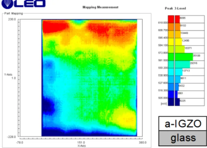
Fig. 13 Example of peak mapping measurement for 440×375 mm2sub- strate after annealing.
Fig. 14 µ-PCD measurement systems for (a) G4.5 (730×920 mm2) and (b) G8 (2160×2460 mm2).
LNBTS test.
6. Mapping Measurements
In the previous study [3], one can extract the optimized con- ditions which give the reasonable TFT mobility by measur- ing the peak values of the decay curves. The peak value mapping on a whole substrate will help to understand the uniformity of the characteristics of the a-IGZO film. For example, it is known that the characteristics do not become uniform by oxygen addition in the process gas for a large glass substrate especially in the case of reactive sputtering method.
Figure 13 shows a mapping measurement result for a 440×375 mm2substrate. The mapping measurements pro- vide useful information on distribution of the film thickness, mobility, and light stability. By checking the mapping of µ-PCD, it is possible to optimize the distribution of vari- ous properties. As shown in Fig. 14,µ-PCD systems corre- sponding to various substrate sizes are already available for measurement of the amorphous oxide semiconductors.
7. Summary
We have investigated the µ-PCD responses from the (a- IGZO thin films. The time constant extracted by the slopes of the slow part of the reflectivity signals were compared
ing for the IGZO-TFTs fabrication.
References
[1] K. Nomura, H. Ohta, A. Takagi, T. Kamiya, M. Hirano, and H.
Hosono, “Room-temperature fabrication of transparent flexible thin- film transistors using amorphous oxide semiconductors,” Nature, vol.432, pp.488–492, Nov. 2004.
[2] S. Yasuno, T. Kugimiya, S. Morita, A. Miki, F. Ojima, and S. Sumie,
“Correlation of photoconductivity response of amorphous In–Ga–
Zn–O films with transistor performance using microwave photocon- ductivity decay method,” Appl. Phys. Lett., vol.98, no.10 pp.102107, 2011.
[3] S. Yasuno, T. Kita, S. Morita, T. Kugimiya, K. Hayashi, and S.
Sumie, “Transient photoconductivity responses in amorphous In–
Ga–Zn–O films,” J. Appl. Phys., vol.112, no.5, pp.053715, 2012.
[4] Y. Kim, S. Kim, W. Kim, M. Bae, H. K. Jeong, D. Kong, S.
Choi, D. M. Kim, and D. H. Kim, “Amorphous InGaZnO thin-film transistors—Part II: Modeling and simulation of negative bias il- lumination stress-induced instability,” IEEE Trans. Electron. Dev., vol.59, no.10, pp.2699–2706, Oct. 2012.
[5] H. Oh, S. M. Yoon, M. K. Ryu, C. S. Hwang, S. Yang, and S. H. K.
Park, “Photon-accelerated negative bias instability involving sub- gap states creation in amorphous In–Ga–Zn–O thin film transistor,”
Appl. Phys. Lett., vol.97, no.18, pp.183502, 2010.
[6] D. P. Gosain and T. Tanaka, “Instability of amorphous indium gal- lium zinc oxide thin film transistors under light illumination,” Jpn.
J. Appl. Phys., vol.48, no.3S2, pp.03B018, Mar. 2009.
[7] K. Takechi, M. Nakata, T. Eguchi, H. Yamaguchi, and S. Kaneko,
“Comparison of ultraviolet photo-field effects between hydro- genated amorphous silicon and amorphous InGaZnO4thin-film tran- sistors,” Jpn. J. Appl. Phys., vol.48, no.1R, pp.010203, Jan. 2009.
[8] C. S. Chuang, T. C. Fung, B. G. Mullins, K. Nomura, T. Kamiya, H. P. D. Shieh, H. Hosono, and J. Kanicki, “Photosensitivity of amorphous IGZO TFTs for active-matrix flat-panel displays,” SID Int. Symp. Digest Tech. Papers, vol.39, no.1, pp.1215–1218, May 2008.
[9] T. C. Fung, C. S. Chuang, K. Nomura, H. P. D. Shieh, H. Hosono, and J. Kanicki, “Photofield-effect in amorphous In–Ga–Zn–O (a- IGZO) thin-film transistors,” J. Inf. Disp., vol.9, no.4, pp.21–29, 2008.
[10] S. Sumie, F. Ojima, K. Yamashita, K. Iba, and H. Hashizume, “Life- time mapping technique for ultrathin silicon-on-insulator wafers,” J.
Electrochem. Soc., vol.152, no.1, pp.G99–G106, 2005.
[11] Y. F. Chen, “Stretched-exponential law for carrier capture kinetics of a trapping center in compensated amorphous silicon,” Phys. Rev.
B, vol.40, pp.3437, 1989.
[12] J. Reemts and A. Kittel, “Persistent photoconductivity in highly porous ZnO films,” J. Appl. Phys., vol.101, no.1, pp.013709, 2007.
[13] D. S. Ginger and N. C. Greenham, “Charge injection and transport in films of CdSe nanocrystals,” J. Appl. Phys., vol.87, no.3, pp.1361,
and T. Kugimiya, “Evaluation of sub-gap states in amorphous In–
Ga–Zn–O thin films treated with various process conditions,” Proc.
MRS, vol.1633, pp.55–60, 2014.
[19] A. Hino, Y. Takanashi, H. Tao, S. Morita, M. Ochi, H. Goto, K.
Hayashi, and T. Kugimiya, “Effects of thermal annealing on varia- tions of electron traps in the channel region of amorphous In–Ga–
Zn–O thin film transistor,” J. Vac. Sci. Technol. B, vol.32, no.3, pp.031210, 2014.
[20] A. Hino, S. Morita, S. Yasuno, T. Kishi, K. Hayashi, and T. Kugimiya, “Effect of H and OH desorption and diffusion on electronic structure in amorphous In–Ga–Zn–O metal-oxide- semiconductor diodes with various gate insulators,” J. Appl. Phys., vol.112, no.11, pp.114515, 2012.
[21] H. J. Kim, S. Y. Park, H. Y. Jung, B. G. Son, C. K. Lee, C. K. Lee, J. H. Jeong, Y. G. Mo, K. S. Son, M. K. Ryu, S. Lee, and J. K.
Jeong, “Role of incorporated hydrogen on performance and photo- bias instability of indium gallium zinc oxide thin film transistors,” J.
Phys. D, vol.46, no.5, pp.055104, Feb. 2013.
[22] Y. S. Rim, W. Jeong, B. D. Ahn, and H. J. Kim, “Defect reduc- tion in photon-accelerated negative bias instability of InGaZnO thin- film transistors by high-pressure water vapor annealing,” Appl. Phys.
Lett., vol.102, no.14, pp.143503, 2013.
[23] D. W. Kwon, J. H. Kim, J. S. Chang, S. W. Kim, W. Kim, J. C. Park, C. J. Kim, and B. G. Park, “Light effect on negative bias-induced instability of HfInZnO amorphous oxide thin-film transistor,” IEEE Trans. Electron. Dev., vol.58, no.4, pp.1127–1133, Apr. 2011.
[24] V. Quemener, L. Vines, E. V. Monakhov, and B. G. Svensson, “Evo- lution of deep electronic states in ZnO during heat treatment in oxygen- and zinc-rich ambients,” Appl. Phys. Lett., vol.100, no.11, pp.112108, 2012.
[25] W. Matangi, F. D. Auret, W. E. Meyer, M. J. Legodi, P. J. Janse van Rensburg, S. M. M. Coelho, M. Diale, and J. M. Nel, “Effect of hydrogen, oxygen, and argon annealing on the electrical proper- ties of ZnO and ZnO devices studied by current-voltage, deep level transient spectroscopy, and Laplace DLTS,” J. Appl. Phys., vol.111, no.9, pp.094504, 2012.
[26] A. Hupfer, C. Bhoodoo, L. Vines, and B. G. Svensson, “The E3 center in zinc oxide; evidence for involvement of hydrogen,” Mater.
Res. Soc. Symp. Proc. vol.1633 (in press).
respectively. He is a researcher of Electronics research laboratory at Kobe Steel, Ltd. He is currently engaged in the development of thin film material for flat panel displays.
Shinya Morita received the B.Sci and M.Sci degrees in physics from Hiroshima University in 2005 and 2007 respectively. Since he joined Kobe Steel, LTD., Kobe Japan in 2007, he has extensively explored new metal film materials for interconnection of FPD. He has involved himself in the studies on development new ox- ide materials and fabrication processes of ox- ide TFTs for FPD. He received the Outstanding Poster Paper Award of IDW in 2010 for research of Oxide semiconductor materials.
Yasuyuki Takanashi received the B.Eng.
and M.Eng. degrees in Materials Science from University of Hyogo in 2007 and 2009, respec- tively. In 2009, he joined Kobelco Research In- stitute, Inc., Kobe, Japan, and has been working on semiconductor analysis. Since 2013 joined a project for oxide semiconductor for FPD in Electronics Research Lab. in Kobe steel, Ltd.
Aya Hino received the B. Sci. and M. Sci.
degrees in physics from Tohoku University in 2003 and 2005, respectively. In 2013, she re- ceived the Dr. degrees in Material Science from Tohoku University. Since she joined Kobe Steel, Ltd., Kobe, Japan in 2005, she has extensively explored new alloy films for interconnection for FPD. Since 2009, she has been conducting re- search and development on oxide TFTs. Her current interest is electronic properties of oxide semiconductors.
respectively. He is a senior researcher of Elec- tronics research laboratory at Kobe Steel Ltd.
He is currently engaged in the development of thin film material for flat panel displays.
Kazushi Hayashi received the Master’s de- gree from Osaka University, Japan, in 1992, and joined Kobe Steel, Japan. He was awarded the Doctor’s degree from Osaka University in 1997.
Since he joined Kobe Steel, he has engaged in the research and development of semiconduct- ing materials and devices. His research interest in an oxide TFTs project is electronic properties of amorphous oxide semiconductors.
Toshihiro Kugimiya received the B.S., M.S. and Dr. degrees in electronics engineer- ing from Toyohashi University of Technology in 1991, 1993, and 2011, respectively. In 1993, he joined Kobe Steel, Ltd., Japan, and he has worked on metal interconnections for FPD, es- pecially, Al-alloy film interconnections. Since 2009 when he joined a project for oxide semi- conductor for FPD in Electronics Research Lab.
in Kobe Steel, he has directed the research of Oxide-TFT fabrication process and analyses of Oxide materials and TFTs.