Design of Nanoscale MOSFETs and
Characterization of their Performance by
Device Simulations
著者
山田 辰哉
学位授与大学
東洋大学
取得学位
博士
学位の分野
工学
報告番号
32663甲第356号
学位授与年月日
2014-03-25
URL
http://id.nii.ac.jp/1060/00006728/
Creative Commons : 表示 - 非営利 - 改変禁止 http://creativecommons.org/licenses/by-nc-nd/3.0/deed.jaDesign of Nanoscale MOSFETs and
Characterization of their Performance
by Device Simulations
Tatsuya Yamada
4R10081001
Doctor Course
Bio-Nano Science Fusion Course
Graduate School of Interdisciplinary New Science
Toyo University, Japan
INDEX
CHAPTER 1. INTRODUCTION 1
1.1 Introduction of Silicon-on-Insulator MOSFETs 2
1.2 Disadvantages due to BOX layers 5
1.3 Objectives and Outline of the Thesis 7
CHAPTER 2. QUANTITATIVE EXTRACTION OF ELECTRIC FLUX IN
THE BURIED-OXIDE LAYER AND INVESTIGATION OF ITS EFFECTS
ON MOSFET CHARACTERISTICS 15
2.1 Introduction 16
2.2 Simulation Method and Device Structures 18
2.3 Results and Discussion 20
2.3.1 SOI MOSFETs without GP structures 20
2.3.2 SOI MOSFETs with GP structures 25
2.4 Summary 30
CHAPTER 3. A MODELING OF DRAIN ELECTRIC FLUX PASSING
THROUGH THE BOX LAYER IN SUBTHRESHOLD REGIONS OF SOI
MOSFETS WITH GROUND PLANE STRUCTURES 36
3.1 Introduction 37
3.2 Modeling 39
3.2.1 Approximation for modeling 40
3.2.2 Electric flux analysis using conformal mapping 42
3.2.3 Relationship between the z and ζ planes 44
3.2.4 Relationship between the w and ζ planes 48
3.2.5 Capacitance and electric flux 52
3.3 Verification of Model Validity 55
CHAPTER 4. IMPROVEMENT OF ELECTRICAL CHARACTERISTICS
OF LOCAL BOX MOSFETS BY HEAVILY DOPED STRUCTURES AND
ELUCIDATION OF THE RELATED MECHANISM 67
4.1 Introduction 68
4.2 Device Structure and Simulation Method 70
4.3 Improvement of Subthreshold Characteristics 72
4.4 Suppression of Self-heating effect 80
4.5 Suppression of Kink Effect 83
4.6 Summary 85
CHAPTER 5. SUPPRESSION OF DRAIN-INDUCED BARRIER
LOWERING IN SILICON-ON-INSULATOR MOSFETS THROUGH SOURCE/DRAIN ENGINEERING FOR LOW-OPERATING-POWER
SYSTEM-ON-CHIP APPLICATIONS 90
5.1 Introduction 91
5.2 Device Structures and Simulation Method 92
5.3 Results and Discussion 97
5.4 Proposed Fabrication Process 106
5.5 Summary 109
CHAPTER 6. CONCLUSIONS 115
ACKNOWLEDGEMENT PUBLICATIONS
1
2
1.1 Introduction of Silicon-on-Insulator MOSFETs
Highly functional electronic devices are indispensable to the modern life [1], [2]. The requirements for functions of electronic devices are becoming more complicated year by year, and the improvement of their performances has been always expected [3]. In order to satisfy the requirements maintaining the size of electronic devices, very-large-scale integrated (VLSI) circuits mounted on electronic devices should increase their integration density without increasing their power consumption [4]. Accordingly, metal oxide semiconductor field effect transistors (MOSFETs) in VLSIs should scale down their size avoiding leakage current, and one of the techniques to satisfy the requirements for advanced MOSFETs is silicon-on-insulator (SOI) technology [5].
SOI technology is a technique for forming an oxide layer into the silicon substrate, and the oxide layer is called a buried-oxide (BOX) layer [6]–[8]. Fig. 1-1 (a) shows the schematic cross-sectional views of conventional bulk MOSFETs and (b) SOI MOSFETs. In the SOI MOSFETs, the BOX layer provides the advantages over bulk MOSFETs in low-power, high-speed, and high voltage applications, because they can achieve low junction capacitance, low leakage current, highly robust breakdown voltage and soft error [9], [10] and excellent subthreshold slope (SS) [9]–[19].
The SS is one of the parameters that reflect the leakage current and indicates gate controllability of MOSFETs, and thanks to the BOX layers in SOI MOSFETs, the SSs in SOI MOSFETs are easily kept lower than those in conventional bulk MOSFETs. This advantage of lower SSs in SOI MOSFETs over conventional bulk MOSFETs are explained partially by these theoretical lower limit, and, the lower limits in bulk MOSFETs and those in SOI MOSFETs are derived and compared as follows:
First of all, the expression of the theoretical lower limit of SSs in conventional bluk MOSFETs can be written as follows [11]:
SS!!"# =!!!
! ln 10
!!"#!!!
3
where kB, T, q, CGOX and CD are the Boltzmann constant, a device temperature, the elementary charge, a capacitance of gate oxide and a capacitance of the depletion layer, respectively, and this equation indicates that CD should be kept lower to minimize the SSbulk. These schematic views of capacitances are shown in Fig. 1-2 (a).
Here, the capacitance between parallel plates can be defined as follows:
C =!!! (2)
where ε is the permittivity in a region between the plates, A is a area of each plates and d is the distance between the plates. As a result, the capacitance becomes small when ε is small and d is large. In estimation of CD using this equation, the value of ε is determined by the permittivity of silicon, and the value of d is determined by the thickness of depletion layer that depends on the dopant concentration in the silicon substrate.
Meanwhile, to obtain the theoretical lower limit in long channel SOI MOSFETs, CD in (1) can be replaced by the series capacitance of the body region Cbody and the capacitance of the BOX layer CBOX as shown in Fig. 1-2 (b), and this series capacitance can be derived as follows:
C!"# = !!"#$ !!"#
!!"#$!!!"#. (3)
This capacitance can be easily kept lower than CD, in bulk MOSFETs and it can be explained by the differences in the structures of capacitances and in the scaling. Considering the structure, CBOX can be easily lower than CD, because the BOX layer has lower ε and larger d than the silicon region. The value of ε is 3.9 in the BOX layer, while it is 11.7 in the silicon region. Moreover, d in the BOX layer can be easily controlled by the BOX layer thickness. In addition to this, CSOI is the series capacitance of Cbody and CBOX. In general, the total capacitance
4
becomes lower when the capacitances are connected in series. Considering the scaling, CD increases with the scaling of MOSFETs, because reduction of its depletion layer thickness results from their increased dopant density [20]. It is indicated that the difference between CSOI and CD becomes significant when MOSFETs are scaled. As a result, theoretical lower limit of SS in SOI MOSFETs can be written as follows:
SS!"# =!!!
! ln 10
!!"#!!!"#
!!"# . (4)
Consequently, this SSSOI can be kept lower than SSbulk, which indicates that the BOX layers contribute to the excellent SSs in the SOI MOSFETs.
Fig. 1-1 Schematic cross-sectional views showing the structures of (a) bulk MOSFETs, and (b) SOI MOSFETs.
Fig. 1-2 Schematic views of capacitances in (a) bulk MOSFETs and (b) SOI MOSFETs. BOX GOX n+ (ND) n+ (ND) p (NA) Source Drain Gate Substrate p (NA) BOX GOX n+ (ND) n+ (ND) p (NA) Source Drain Gate Substrate p (NA) (a) (b)
5
1.2 Disadvantages due to BOX layers
However, the BOX layers in the SOI MOSFETs provide several inherent disadvantages such as enhancement of drain-induced barrier lowering (DIBL) via BOX layers [16], [21]–[25]. This enhanced DIBL is the disadvantage that induces extra SS from theoretical SS [22]. This DIBL is induced by the electric flux from the drain to the body region passing through the BOX layers as shown in Fig. 1-3, and this flux lowers the barrier height along the SOI/BOX interface. This penetration of the electric flux results from a lack of the charge in the BOX layer, and thus this DIBL is one of the inherent disadvantages due to the BOX layer. The relation between the DIBL and the flux is discussed in Chapter 2 and 3, and several structures to suppress the DIBL are proposed in Chapter 5.
In addition to the DIBL, the BOX layer provides another inherent disadvantages such as self heating effects (SHEs) [31], [32] which induced by low thermal conductivity of the BOX layer, and kink effect [27], [33] which induced by accumulation of impact-ionized carriers enhanced by the BOX layer.
These disadvantages can be suppressed by improvement of the BOX structure, which take advantage of one of the fabrication method of SOI substrate. In general, there have been several methods to fabricate SOI substrates: UNIBOND substrates in which top and substrate silicon layers are formed separately, then are bonded with each other [34], epitaxial-layer-transfer (ELTRAN) substrates in which top silicon layers are formed using epitaxial growth [35], separation by implantation of oxygen (SIMOX) substrates in which the BOX layers are formed using implantation of oxygen ions [36]. The SIMOX substrates have an advantage that can easily form patterned BOX layers in the substrates, and to suppress the BOX related disadvantages, several structures with this advantage are discussed in Chapter 4.
These disadvantages related to the BOX layers such as the BOX related DIBL, kink effect and SHEs are already known phenomena. However, investigation of detailed mechanism and evaluations of the magnitude of these disadvantages are insufficient, and the proposals of the solutions are also insufficient. Accordingly, I evaluate these BOX layer related disadvantages with
6
mainly focusing on the drawback of the DIBL, and address the proposals of improvement techniques for these disadvantages with device simulations.
Fig. 1-3. Cross-sectional view of a SOI MOSFET in potential distribution and electric flux when strong flux passing from the drain to the body region via the BOX layers. Electric flux is shown with solid lies in the BOX layer, and the flux passing from the drain to the body is highlighted by the open ellipse.
7
1.3 Objectives and Outline of the Thesis
In this thesis, I focused on the BOX related disadvantages, and discussed their phenomena and countermeasure. Accordingly, there are two objectives in this thesis: one is the evaluation of the disadvantage due to the DIBL via BOX layers, and the other is proposal of new device structures to avoid the inherent disadvantages due to the BOX layers. In this thesis, I divided them into four chapters as shown in Fig. 1-4.
The evaluation of the DIBL is described in Chapter 2 and 3. In Chapter 2, I visualized the electric flux distribution in the BOX layers using stream functions, and extracted the electric flux from the drain to the body region quantitatively for the first time. Moreover, I demonstrated the dependence of the amount of electric flux and SS on the BOX layers relative permittivity and thickness, and clarified the relevance of the flux and the DIBL. In Chapter 3, I expanded the discussion of the electric flux mentioned in Chapter 2, and developed a compact model of the electric flux from the drain to the body region in ground plane (GP) SOI MOSFETs [16], [37]–[39]. This model is based on the conformal mapping techniques [40]–[51], and it makes it possible to estimate the amount of the electric flux analytically. I demonstrated the validity of the model by comparing the amount of electric flux determined by the model and the amount extracted by device simulations. These comparisons are demonstrated in terms of the dependence the flux on the thickness of BOX layers, the permittivity in BOX layer, the thickness of SOI layers and the gate length.
The proposals of new device structures to avoid the inherent disadvantages due the BOX layers are described in Chapter 4 and 5. In Chapter 4, I proposed heavily doped silicon between insulator (HDSBI) structures that have local BOX regions and additional doped silicon region, in which acceptors or traps are intentionally introduced. I demonstrated that HDSBI MOSFETs suppress of SCEs and kink effect, which are the disadvantage due to the BOX layer. In Chapter 5, I proposed L-shaped counter-doped source and drain (LCSD) structures that have counter doped regions under the source and drain regions. I demonstrated the
8
suppression of DIBL via BOX layers by the counter doped regions in the proposed structures, and also demonstrate that MOSFETs with the proposed structures have SSs as excellent as those in extremely thin SOI MOSFETs even when SOI layers are thick. Finally in Chapter 6, I concluded this study.
Fig. 1-4 Schematic outline of the thesis.
DIBL via BOX Short Channel Effect Kink Effect Self Heating Effect BOX
Heat Hole
Disadvantages of SOI MOSFETs Disadvantages of SOI MOSFETs
Chapter 2
Visualization and Extraction
Chapter 3 Model Derivation n+ BOX BOX n+ p High density Traps n+ BOX n+ p p p++ p++ Chapter 5
L-shaped Counter Doping Heavily doped local BOXChapter 4
Evaluation of Degradation
9
References
[1] J. B. Kuo and S.-C. Lin, Low-Voltage SOI CMOS VLSI Devices and Circuits. Wiley-Interscience, 2001, p. 424.
[2] W.-K. Chen, The VLSI Handbook (Electrical Engineering Handbook). CRC Press, 1999, p. 1788.
[3] “ITRS Reports.” [Online]. Available: http://www.itrs.net/reports.html. [Accessed: 01-Sep-2013].
[4] G. E. Moore, “Cramming more components onto integrated circuits, Reprinted from Electronics, volume 38, number 8, April 19, 1965, pp.114 ff.,”
IEEE Solid-State Circuits Newsl., vol. 20, no. 3, pp. 33–35, Sep. 2006.
[5] R.-H. Yan, A. Ourmazd, and K. F. Lee, “Scaling the Si MOSFET: from bulk to SOI to bulk,” IEEE Trans. Electron Devices, vol. 39, no. 7, pp. 1704–1710, Jul. 1992.
[6] V. P. Trivedi and J. G. Fossum, “Nanoscale FD/SOI CMOS: thick or thin BOX?,” vol. 26, 2005.
[7] C. Fenouillet-Beranger, T. Skotnicki, S. Monfray, N. Carriere, and F. Boeuf, “Requirements for ultra-thin-film devices and new materials for the CMOS roadmap,” Solid. State. Electron., vol. 48, no. 6, pp. 961–967, Jun. 2004. [8] T. Numata and S.-I. Takagi, “Device Design for Subthreshold Slope and
Threshold Voltage Control in Sub-100-nm Fully Depleted SOI MOSFETs,”
IEEE Trans. Electron Devices, vol. 51, no. 12, pp. 2161–2167, Dec. 2004.
[9] J.-P. Colinge, Silicon-on-Insulator Technology: Materials to VLSI, 2nd ed. Boston: Kluwer, 2004.
[10] J.-P. Colinge, “Subthreshold slope of thin-film SOI MOSFET’s,” IEEE
Electron Device Lett., vol. 7, no. 4, pp. 244–246, Apr. 1986.
[11] S. M. Sze and K. K. Ng, Physics of Semiconductor Devices, 3rd ed. New York: Wiley-Interscience, 2006.
[12] R. Wacquez, M. Vinet, M. Pierre, B. Roche, X. Jehl, O. Cueto, J. Verduijn, G. C. Tettamanzi, S. Rogge, V. Deshpande, B. Previtali, C. Vizioz, S. Pauliac-Vaujour, C. Comboroure, N. Bove, O. Faynot, and M. Sanquer, “Single dopant impact on electrical characteristics of SOI NMOSFETs with effective length down to 10nm,” in 2010 Symposium on VLSI Technology, 2010, pp. 193–194.
10
[13] Q. Liu, A. Yagishita, N. Loubet, A. Khakifirooz, P. Kulkarni, T. Yamamoto, K. Cheng, M. Fujiwara, J. Cai, D. Dorman, S. Mehta, P. Khare, K. Yako, Y. Zhu, S. Mignot, S. Kanakasabapathy, S. Monfray, F. Boeuf, C. Koburger, H. Sunamura, S. Ponoth, A. Reznicek, B. Haran, A. Upham, R. Johnson, L. F. Edge, J. Kuss, T. Levin, N. Berliner, E. Leobandung, T. Skotnicki, M. Hane, H. Bu, K. Ishimaru, W. Kleemeier, M. Takayanagi, B. Doris, and R. Sampson, “Ultra-thin-body and BOX (UTBB) fully depleted (FD) device integration for 22nm node and beyond,” in 2010 Symposium on VLSI
Technology, 2010, pp. 61–62.
[14] A. Khakifirooz, K. Cheng, A. Reznicek, T. Adam, N. Loubet, H. He, J. Kuss, J. Li, P. Kulkarni, S. Ponoth, R. Sreenivasan, Q. Liu, B. Doris, and G. Shahidi, “Scalability of Extremely Thin SOI (ETSOI) MOSFETs to Sub-20-nm Gate Length,” IEEE Electron Device Lett., vol. 33, no. 2, pp. 149–151, Feb. 2012.
[15] S. Burignat, D. Flandre, M. K. Md Arshad, V. Kilchytska, F. Andrieu, O. Faynot, and J.-P. Raskin, “Substrate impact on threshold voltage and subthreshold slope of sub-32nm ultra thin SOI MOSFETs with thin buried oxide and undoped channel,” Solid. State. Electron., vol. 54, no. 2, pp. 213– 219, Feb. 2010.
[16] C. Fenouillet-Beranger, S. Denorme, P. Perreau, C. Buj, O. Faynot, F. Andrieu, L. Tosti, S. Barnola, T. Salvetat, X. Garros, M. Cassé, F. Allain, N. Loubet, L. Pham-Nguyen, E. Deloffre, M. Gros-Jean, R. Beneyton, C. Laviron, M. Marin, C. Leyris, S. Haendler, F. Leverd, P. Gouraud, P. Scheiblin, L. Clement, R. Pantel, S. Deleonibus, and T. Skotnicki, “FDSOI devices with thin BOX and ground plane integration for 32nm node and below,” Solid. State. Electron., vol. 53, no. 7, pp. 730–734, Jul. 2009.
[17] A. Khakifirooz, K. Cheng, T. Nagumo, N. Loubet, T. Adam, A. Reznicek, J. Kuss, D. Shahrjerdi, R. Sreenivasan, S. Ponoth, H. He, P. Kulkarni, Q. Liu, P. Hashemi, P. Khare, S. Luning, S. Mehta, J. Gimbert, Y. Zhu, Z. Zhu, J. Li, A. Madan, T. Levin, F. Monsieur, T. Yamamoto, S. Naczas, S. Schmitz, S. Holmes, C. Aulnette, N. Daval, W. Schwarzenbach, B.-Y. Nguyen, V. Paruchuri, M. Khare, G. Shahidi, and B. Doris, “Strain engineered extremely thin SOI (ETSOI) for high-performance CMOS,” in 2012 Symposium on
11
[18] C. Le Royer, A. Villalon, M. Casse, D. Cooper, J. Mazurier, B. Previtali, C. Tabone, P. Perreau, J.-M. Hartmann, P. Scheiblin, F. Allain, F. Andrieu, O. Weber, P. Batude, O. Faynot, and T. Poiroux, “First demonstration of ultrathin body c-SiGe channel FDSOI pMOSFETs combined with SiGe(:B) RSD: Drastic improvement of electrostatics (Vth,p tuning, DIBL) and transport (µ0, Isat) properties down to 23nm gate length,” in 2011
International Electron Devices Meeting, 2011, pp. 16.5.1–16.5.4.
[19] C. Riddet, C. Alexander, A. R. Brown, S. Roy, and A. Asenov, “Simulation of ‘Ab Initio’ Quantum Confinement Scattering in UTB MOSFETs Using Three-Dimensional Ensemble Monte Carlo,” IEEE Trans. Electron Devices, vol. 58, no. 3, pp. 600–608, Mar. 2011.
[20] R. H. Dennard, F. H. Gaensslen, V. L. Rideout, E. Bassous, and A. R. LeBlanc, “Design of ion-implanted MOSFET’s with very small physical dimensions,” IEEE J. Solid-State Circuits, vol. 9, no. 5, pp. 256–268, Oct. 1974.
[21] S. Abe, Y. Miyazawa, Y. Nakajima, T. Hanajiri, T. Toyabe, and T. Sugano, “Suppression of DIBL in deca-nano SOI MOSFETs by controlling permittivity and thickness of BOX layers,” in 2009 10th International
Conference on Ultimate Integration of Silicon, 2009, pp. 329–332.
[22] T. Hanajiri, T. Toyabe, and T. Sugano, “Suppression of short channel effects by full inversion in deep sub-micron gate SOI MOSFETs,” Solid. State.
Electron., vol. 45, no. 12, pp. 2077–2081, Dec. 2001.
[23] T. Hanajiri, M. Niizato, K. Aoto, T. Toyabe, Y. Nakajima, T. Morikawa, and T. Sugano, “Scaling rules for SOI MOSFETs operating in the fully inverted mode,” Solid. State. Electron., vol. 48, no. 10–11, pp. 1943–1946, Oct. 2004. [24] T. Yamada, S. Abe, Y. Nakajima, T. Hanajiri, T. Toyabe, and T. Sugano,
“Quantitative Extraction of Electric Flux in the Buried-Oxide Layer and Investigation of its Effects on MOSFET Characteristics,” IEEE Trans.
Electron Devices, vol. 60, no. 12, pp. 3996 – 4001, 2013.
[25] T. Yamada, Y. Nakajima, T. Hanajiri, and T. Sugano, “Suppression of Drain-Induced Barrier Lowering in Silicon-on-Insulator MOSFETs Through Source/Drain Engineering for Low-Operating-Power System-on-Chip Applications,” IEEE Trans. Electron Devices, vol. 60, no. 1, pp. 260–267, Jan. 2013.
12
[26] K. Kajiwara, Y. Nakajima, T. Hanajiri, T. Toyabe, and T. Sugano, “Characterization of Distribution of Trap States in Silicon-on-Insulator Layers by Front-Gate Characteristics in n-Channel SOI MOSFETs,” IEEE
Trans. Electron Devices, vol. 55, no. 7, pp. 1702–1707, Jul. 2008.
[27] Y. Nakajima, K. Sasaki, T. Hanajiri, T. Toyabe, T. Morikawa, and T. Sugano, “Confirmation of electric properties of traps at silicon-on-insulator (SOI)/buried oxide (BOX) interface by three-dimensional device simulation,”
Phys. E Low-dimensional Syst. Nanostructures, vol. 24, no. 1–2, pp. 92–95,
2004.
[28] Y. Nakajima, Y. Watanabe, T. Hanajiri, T. Toyabe, and T. Sugano, “Local-Stress-Induced Trap States in SOI Layers With Different Levels of Roughness at SOI/BOX Interfaces,” IEEE Electron Device Lett., vol. 32, no. 3, pp. 237–239, Mar. 2011.
[29] Y. Nakajima, H. Tomita, K. Aoto, N. Ito, T. Hanajiri, T. Toyabe, T. Morikawa, and T. Sugano, “Characterization of Trap States at Silicon-On-Insulator (SOI)/Buried Oxide (BOX) Interface by Back Gate Transconductance Characteristics in SOI MOSFETs,” Jpn. J. Appl. Phys., vol. 42, no. Part 1, No. 4B, pp. 2004–2008, Apr. 2003.
[30] Y. Nakajima, T. Toda, T. Hanajiri, T. Toyabe, and T. Sugano, “In-depth profiling of electron trap states in silicon-on-insulator layers and local mechanical stress near the silicon-on-insulator/buried oxide interface in separation-by-implanted-oxygen wafers,” J. Appl. Phys., vol. 108, no. 12, p. 124505, Dec. 2010.
[31] M. B. Kleiner, S. A. Kuhn, and W. Weber, “Thermal conductivity measurements of thin silicon dioxide films in integrated circuits,” IEEE
Trans. Electron Devices, vol. 43, no. 9, pp. 1602–1609, 1996.
[32] Han Xiao, Ru Huang, Jiale Liang, Hongwei Liu, Yu Tian, Runsheng Wang, and Yangyuan Wang, “The Localized-SOI MOSFET as a Candidate for Analog/RF Applications,” IEEE Trans. Electron Devices, vol. 54, no. 8, pp. 1978–1984, Aug. 2007.
[33] J.-Y. Choi and J. G. Fossum, “Analysis and control of floating-body bipolar effects in fully depleted submicrometer SOI MOSFET’s,” IEEE Trans.
13
[34] M. Bruel, “Silicon on insulator material technology,” Electron. Lett., vol. 31, no. 14, 1995.
[35] T. Yonehara, K. Sakaguchi, and N. Sato, “Epitaxial layer transfer by bond and etch back of porous Si,” Appl. Phys. Lett., vol. 64, no. 16, p. 2108, Apr. 1994.
[36] K. Izumi, M. Doken, and H. Ariyoshi, “C.M.O.S. devices fabricated on buried SiO2 layers formed by oxygen implantation into silicon,” Electron.
Lett., vol. 14, no. 18, p. 593, 1978.
[37] Z. Ren, M. Ieong, J. Cai, J. Holt, D. Boyd, R. Mo, H. Yin, O. Dokumaci, S. Kawanaka, T. Sato, P. Ronsheim, J. Wang, C. Y. Sung, and W. Haensch, “Selective epitaxial channel ground plane thin SOI CMOS devices,” in IEEE
InternationalElectron Devices Meeting, 2005. IEDM Technical Digest., 2005,
pp. 733–736.
[38] H.-S. P. Wong, D. J. Frank, and P. M. Solomon, “Device design considerations for double-gate, ground-plane, and single-gated ultra-thin SOI MOSFET’s at the 25 nm channel length generation,” in International
Electron Devices Meeting 1998. Technical Digest (Cat. No.98CH36217),
1998, pp. 407–410.
[39] L. Grenouillet, P. Khare, J. Gimbert, M. Hargrove, M. A. Jaud, Q. Liu, Y. Le Tiec, R. Wacquez, N. Loubet, K. Cheng, S. Holmes, S. Liu, T. Hook, S. Teehan, J. Guilford, S. Schmitz, P. Kulkarni, J. Kuss, M. Terrizzi, S. Luning, B. Doris, and M. Vinet, “Ground plane optimization for 20nm FDSOI transistors with thin Buried Oxide,” in 2012 IEEE International SOI
Conference (SOI), 2012, pp. 1–2.
[40] T. Ernst, C. Tinella, C. Raynaud, and S. Cristoloveanu, “Fringing fields in sub-0.1 µm fully depleted SOI MOSFETs: optimization of the device architecture,” Solid. State. Electron., vol. 46, no. 3, pp. 373–378, Mar. 2002. [41] T. Ernst, R. Ritzenthaler, O. Faynot, and S. Cristoloveanu, “A Model of
Fringing Fields in Short-Channel Planar and Triple-Gate SOI MOSFETs,”
IEEE Trans. Electron Devices, vol. 54, no. 6, pp. 1366–1375, Jun. 2007.
[42] A. Bansal, B. C. Paul, and K. Roy, “Modeling and Optimization of Fringe Capacitance of Nanoscale DGMOS Devices,” IEEE Trans. Electron Devices, vol. 52, no. 2, pp. 256–262, Feb. 2005.
14
[43] H. Børli, S. Kolberg, and T. A. Fjeldly, “Capacitance modeling of short-channel double-gate MOSFETs,” Solid. State. Electron., vol. 52, no. 10, pp. 1486–1490, Oct. 2008.
[44] U. Monga and T. A. Fjeldly, “Compact Subthreshold Current Modeling of Short-Channel Nanoscale Double-Gate MOSFET,” IEEE Trans. Electron
Devices, vol. 56, no. 7, pp. 1533–1537, Jul. 2009.
[45] U. Monga, H. Børli, and T. A. Fjeldly, “Compact subthreshold current and capacitance modeling of short-channel double-gate MOSFETs,” Math.
Comput. Model., vol. 51, no. 7–8, pp. 901–907, Apr. 2010.
[46] A. Kloes and M. Weidemann, “Self-consistent 2D compact modeling of nanoscale bulk MOSFETs,” Solid. State. Electron., vol. 51, no. 5, pp. 739– 748, May 2007.
[47] A. Kloes, M. Weidemann, D. Goebel, and B. T. Bosworth, “Three-Dimensional Closed-Form Model for Potential Barrier in Undoped FinFETs Resulting in Analytical Equations for Vt and Subthreshold Slope,”
IEEE Trans. Electron Devices, vol. 55, no. 12, pp. 3467–3475, Dec. 2008.
[48] A. Bansal and K. Roy, “Analytical Subthreshold Potential Distribution Model for Gate Underlap Double-Gate MOS Transistors,” IEEE Trans.
Electron Devices, vol. 54, no. 7, pp. 1793–1798, Jul. 2007.
[49] H. Borli, S. Kolberg, T. A. Fjeldly, and B. Iniguez, “Precise Modeling Framework for Short-Channel Double-Gate and Gate-All-Around MOSFETs,” IEEE Trans. Electron Devices, vol. 55, no. 10, pp. 2678–2686, Oct. 2008.
[50] S. Kolberg, H. Børli, and T. A. Fjeldly, “Modeling, verification and comparison of short-channel double gate and gate-all-around MOSFETs,”
Math. Comput. Simul., vol. 79, no. 4, pp. 1107–1115, Dec. 2008.
[51] S.-H. Kim, J. G. Fossum, and J.-W. Yang, “Modeling and Significance of Fringe Capacitance in Nonclassical CMOS Devices With Gate–Source/Drain Underlap,” IEEE Trans. Electron Devices, vol. 53, no. 9, pp. 2143–2150, Sep. 2006.
15
Chapter 2. Quantitative Extraction of Electric
Flux in the Buried-Oxide Layer and
Investigation of its Effects on MOSFET
16
2.1 Introduction
The evaluation of the DIBL is described in Chapter 2 and 3, and in this chapter, I extract electric flux in the buried-oxide (BOX) layer quantitatively.
Silicon-on-insulator (SOI) technology has a number of advantages over conventional bulk technology, including low junction capacitance, minimal leakage current, high gate controllability and highly robust breakdown voltage [1], [2]. As a result, it can be used to efficiently reduce the gate length of MOSFETs [3] and has been widely adopted in the scaling of modern VLSI circuits. However, BOX layers in SOI MOSFETs have inherent disadvantages, such as low thermal conductivity [4], [5], trap state formation at the SOI/BOX interface [6]–[8] and enhanced drain-induced barrier lowering (DIBL) [9]–[14]. The author’s group previously focused on DIBL in relation to BOX layers [15] and reported that such lowering is suppressed by reducing the layer thickness TBOX [16]. The effects of electric flux detouring from the drain via the BOX layer were also discussed based on visualization with variations in the relative permittivity of BOX layers kBOX as well as TBOX [17]. Other researchers have also focused on DIBL in relation to the BOX layer, and the dependence of subthreshold slopes (SSs) on kBOX and TBOX has been approximately estimated [18]. The negative effects of drain electric field detouring through the BOX layer have also been reported [10]– [14], while the results of other studies have indicated remarkable benefits from the reduction of the gate length LG achieved by field suppression due to thinning of the BOX layer in recent ultra-thin-body and BOX (UTBB) SOI MOSFETs [19], [20]. However, the amount of electric flux detouring from the drain to the body region via the BOX layer (referred to here for simplicity as detouring electric flux) and the relationship between this amount and the resultant DIBL have not been investigated quantitatively. One method of determining the exact amount of such flux is to quantitatively visualize flux lines so that their density is proportional to the extent of the flux. Although equipotential lines in devices have often been visualized in MOSFET fields [10]–[13], [21], exact visualization of precise electric field lines and electric flux lines perpendicularly intersecting
17
equipotential lines has been minimal except in previous papers by the authors [15], [17]. While some reports have covered the visualization of electric fields in BOX layers with lines visualized schematically [10], [11], [13], quantitative analysis of the field using schematically visualized images remains difficult. Meanwhile, plausible electric field lines have been visualized in some studies using a stream tracing technique [14], [22], but quantitative analysis using such lines is also difficult. This technique is an effective method for visualizing and estimating the destinations of lines approximately, but these lines are very sensitive to the arbitrary initial positions of streams, and their density does not indicate the amount of flux.
Against such a background, numerically precise electric flux lines in the BOX layer were visualized in this study, and the amount of detouring electric flux was evaluated quantitatively for the first time using stream functions [23], [24] with focus on their dependence on kBOX and TBOX. Such precision in the estimation of flux is effective for discussing the influence of drain electric field detouring through the BOX layer on MOSFET characteristics separately from other effects.
18
2.2 Simulation Method and Device Structures
The electrical characteristics of SOI MOSFETs were simulated using Synopsys’ Sentaurus TCAD (technology computer-aided design) software [25], while electric flux visualization and quantification were performed by calculating Sentaurus outputs using stream functions, and additional information on this simulator is described in the appendix.
In this study, the electric flux density (rather than the electric field) in the BOX layer was visualized because it is directly determined by the electrical charge according to Gauss’s law.
Table 2-1 Device parameters of MOSFETs.
Parameter Symbol Value
Physical gate length LG 100 nm
Gate oxide thickness TGOX 1.3 nm
SOI layer thickness TSOI 20 nm
BOX layer thickness TBOX 10 – 119 nm
Relative permittivity in BOX layer kBOX 1.0 – 11.9
Acceptor density in SOI layer NA 1017 cm-3
Acceptor density in GP substrate NAGP 1019 cm-3 Donor density in drain/source region ND 1020 cm-3
19
Table 2-1 shows the device parameters used in the simulations. To clarify the influence of the detouring electric flux separately from other effects, device structure features such as shallow junctions [26], halo doping [27], retrograde doping [28] and ground plane (GP) doping [20] were not used. In addition, the physical gate length LG, the SOI layer thickness TSOI, the gate dielectric thickness TGOX and the impurity concentrations NA and ND were fixed. In the simulation, LG and TSOI were assumed to be 100 and 20 nm, respectively, although both have been scaled down to less than 25 nm and around 5 nm, respectively, in advanced UTB SOI MOSFETs [3], [29] in which certain phenomena peculiar to ultra-thin films were remarkable: 1) mobility was degraded by surface roughness, confined acoustic phonons and Coulomb scattering [30], and 2) the threshold voltage was shifted as a result of quantum effects [31]. However, these complicated phenomena were suppressed in the present study to allow focus on the effects of detouring electric flux. Even though these phenomena were suppressed, the essential nature of the effects was not impaired in the MOSFETs used in this study because the ratio of LG to TSOI was maintained to approximately 5 in these transistors as in advanced UTB SOI MOSFETs. Additionally, in order to elucidate the behavior of electric flux in the BOX layer, wider ranges of kBOX and TBOX than those of modern UTB SOI MOSFETs [32] were chosen based on feasible substrates on which various advanced MOSFETs are fabricated. Silicon-on-quartz (SOQ) MOSFETs [33] can be seen as SOI MOSFETs with large TBOX values in terms of electrical characteristics, and such large values provide an advantage in terms of robust breakdown voltage in high-voltage applications [21]. In relation to kBOX, silicon-on-sapphire (SOS) [34] MOSFETs, silicon-on-diamond (SOD) [35] MOSFETs and silicon-on-nothing (SON) [36] MOSFETs have significantly different kBOX values from those of conventional SOI MOSFETs.
20
2.3 Results and Discussion
2.3.1 SOI MOSFETs without GP structures
Figure 2-1 shows potential distribution in SOI layers, BOX layers and substrates along with electric flux lines in BOX layers and current flow lines in SOI layers to clarify the distribution of detouring electric flux. Each flux line indicates 5 pC/m. The gate voltage is set as 0 V to minimize its effect and maintain the influence of drain electric flux. These results indicate that large kBOX and TBOX values enhance detouring electric flux. When TBOX is 119 nm in Figs. 2-1 (a) and (b), some flux reaches the body region detouring through the thick BOX layer rather than being terminated by the substrate. kBOX increases the number of whole electric flux lines from the drain but does not significantly affect their destinations (this is particularly seen in Figs. 2-1 (a) and (b)). The figures also show that when kBOX and TBOX become large, there is a close correlation between detouring electric flux and the current flow lines formed at the SOI/BOX interface. Consequently, to support the effective suppression of leakage current at the SOI/BOX interface, the causative detouring electric flux should be investigated quantitatively.
21
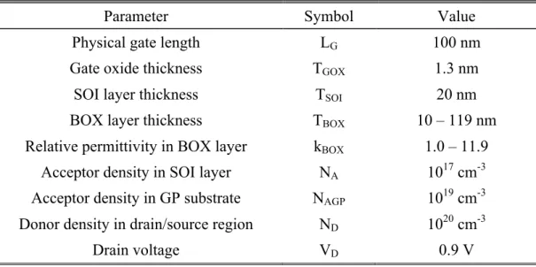
Fig. 2-1 Cross-sectional views of SOI MOSFETs in potential distribution, current flow and electric flux when VG = 0 V with values of LG = 100 nm for (a) kBOX = 1.0 and TBOX = 119 nm, (b) kBOX = 11.9 and TBOX = 119 nm, (c) kBOX = 1.0 and TBOX = 39 nm, and (d) kBOX = 11.9 and TBOX = 39 nm. Potential is indicated by colors, and current flow is shown with solid lines in SOI layers. Electric flux is shown with solid lines in BOX layers, and electric flux reaching the body region via BOX layers is shown with red lines.
22
Figure 2-2 shows the dependence of the amount of detouring electric flux on kBOX and TBOX. In actual application, the flux passing through the SOI/BOX interface as shown by the red lines in Fig. 2-1 was selected, and the amount was calculated quantitatively using stream functions. Figure 2-2 shows that the amount of detouring electric flux increases monotonically with respect to kBOX and TBOX, which confirms the tendency of the flux seen in Fig. 2-1. The enhancement of DIBL due to the presence of the thick BOX layer has already been reported [10]–[14], but this study represented the first quantification of the detouring electric flux that leads to leakage current in SOI MOSFETs: the flux lines normally intersect equipotential lines exactly, the line density is proportional to the amount of flux, and this amount can be calculated precisely using stream functions for variations of kBOX and TBOX.
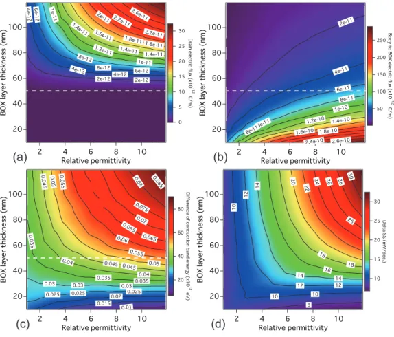
Fig. 2-2. kBOX- and TBOX-related dependences of the amount of electric flux reaching the body region through BOX layers when VG = 0 V.
23
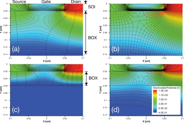
To elucidate the relationship between detouring electric flux and the resultant leakage current, DIBL and this flux were examined for various values of kBOX and TBOX as shown in Fig. 2-3. DIBL is defined as the difference between the barrier height when VD is 0.90 V and that when VD is 0.05 V along the SOI/BOX interface, as shown in Fig. 2-3 (a). It should be noted that the DIBL defined here is different from the other type often referenced in the semiconductor field, which is defined as the threshold voltage difference. In Fig. 2-3, DIBL is shown as conduction band energy instead of potential. Figure 2-3 (b) illustrates the dependence of DIBL on kBOX and TBOX. These figures indicate that DIBL increases more or less monotonically with respect to the two values. As a result, detouring electric flux has a similar dependence on kBOX and TBOX.
Fig. 2-3. (a) Conduction band energy distribution along the SOI/BOX interface when VG = 0 V. The drain voltages are set as 0.90 and 0.05 V. (b) The kBOX- and TBOX-related dependences of the difference between the conduction band energy when VD is 0.90 V and that when VD is 0.05 V.
Source (b) (a) DIBL Drain Gate
Conduction band ener
24
To examine how DIBL along the SOI/BOX interface affects MOSFET characteristics, the SS (which reflects the leakage current in MOSFETs) and its dependence on kBOX and TBOX were investigated as shown in Fig. 2-4. Figure 2-4 (a) shows simulated SSs for MOSFETs with various values of kBOX and TBOX. In contrast, Fig. 2-4 (b) shows the theoretical lower limits of SSs in long-channel SOI MOSFETs as determined from the ratio of gate oxide capacitance, body capacitance and BOX capacitance [2].
S =!! ! ! ln 10 1 + !! !!" !!"# !!"#!!! (1)
where kB is the Boltzmann constant, T is the temperature, q is the elementary charge, CB is the capacitance of the body region, COX is the capacitance of the gate oxide and CBOX is the capacitance of the BOX layer.
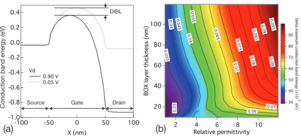
Fig. 2-4. The kBOX- and TBOX-related dependences of (a) simulated SS, (b) theoretical long-channel SS, and (c) the difference between simulated and theoretical SSs when VG = 0 V.
25
In Figs. 2-4 (a) and (b), all the other device parameters are the same as those in Table 2-1. To highlight the extra enhancement of SSs due to DIBL, Fig. 2-4 (c) shows the difference between the simulated SSs in Fig. 2-4 (a) and the theoretical lower limits of the SSs in Fig. 2-4 (b). It indicates that the dependence of the extra enhancement increases monotonically with kBOX and TBOX, and that such dependence is similar to that of DIBL as shown in Fig. 2-3 (b). The extra enhancement of SSs shown in Fig. 2-4 (c) and the amount of detouring electric flux in Fig. 2-2 also have similar dependences on kBOX and TBOX.
In summary, the amount of detouring electric flux shown in Fig. 2-2, DIBL at the SOI/BOX interface in Fig. 2-3 (b), and the extra enhancement of SSs in Fig. 2-4 (c) have similar dependences on kBOX and TBOX. These results indicate that when kBOX and TBOX become larger, flux detours from the drain to the body region via the BOX layer, then DIBL at the SOI/BOX interface increases, and subsequently a leakage current path is formed near the SOI/BOX interface, leading to SSs enhancement in SOI MOSFETs.
2.3.2 SOI MOSFETs with GP structures
In the work detailed in the previous section, complicated doping profiles in devices including GP structures were avoided to help clarify the effect of drain electric flux. Nevertheless, regardless of drain electric flux-related relationships, the DIBL and SSs discussed in the previous section are valid and interesting if these structure features are applied. In particular, GP structures have especially strong effects on potential distribution in BOX layers due to their heavily doped substrate, and dramatically change the behavior of electric flux in such layers. To confirm the validity of the relationship, the electric characteristics of MOSFETs with GP structures were simulated under the conditions shown in Figs. 2–4 except when GP regions with acceptors of 1019 cm-3 were formed.
26
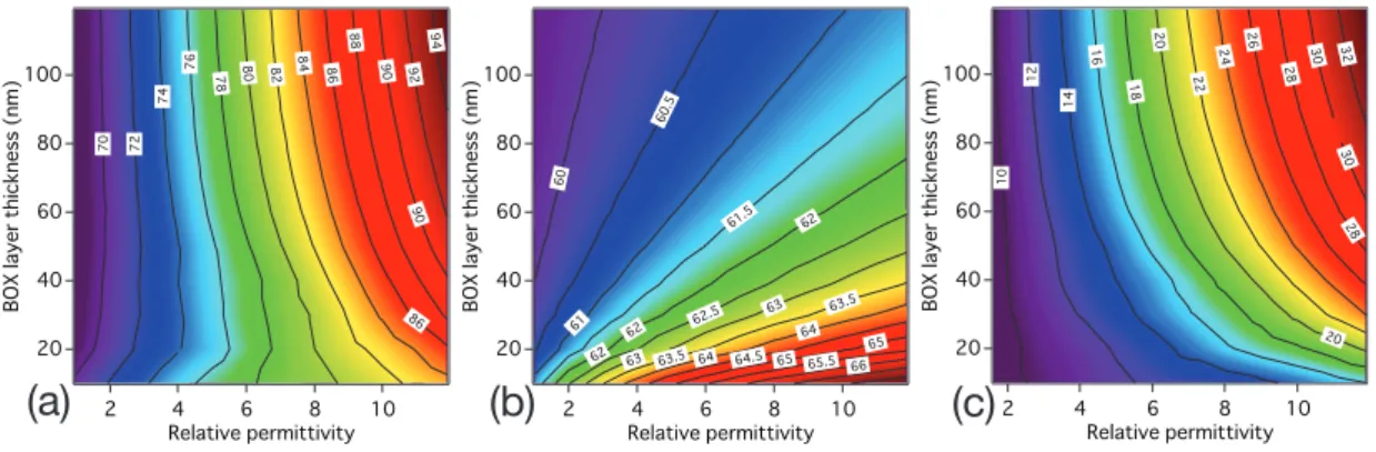
Fig. 2-5. The kBOX– and TBOX–related dependencies of (a) the amount of electric flux from the drain to the body region through the BOX layer, (b) the amount of electric flux from the body to the substrate through the BOX layer, (c) the difference in the conduction band energy along the SOI/BOX interface when VD is 0.90 V and that when VD is 0.05 V, and (d) the difference between simulated and theoretical lower limit of SSs.
27
Figure 2-5 shows the kBOX- and TBOX-related dependences on the amount of electric flux, DIBL and SS differences. In SOI MOSFETs with GP structures, electric flux behavior can be explained in relation to the amount of electric flux passing from the drain to the body and from the body to the substrate. Fig. 2-5 (a), (b) and (c) demonstrate that when the BOX layer is thicker than around 50 nm, the flux from the drain to the body as shown in Fig. 2-5 (a) dominates the differences in conduction band energies as shown in Fig.2-5 (c), and conversely, when it is thinner than around 50 nm, this domination is suppressed, and the flux from the body to the substrate as shown in Fig. 2-5 (a) dominates the difference in Fig. 2-5 (c). The electric flux behavior here can be understood as follows: as the BOX layer becomes thinner, the electric flux from the drain reaches the substrate rather than the body more easily, and is enhanced by the GP structures’ lowering of substrate potential. Consequently, the amount of flux reaching the body decreases. In addition, as the BOX layer becomes thinner, flux from the body to the substrate is influenced more.
Figure 2-5 (d) shows the difference between the simulated SSs of the SOI MOSFETs with GP structures and the theoretical lower limits of the SSs shown in Fig. 2-4 (b). This difference has a tendency similar to that of the conduction band energies shown in Fig. 2-5 (c): they have kBOX and TBOX dependence in high-TBOX regions, and weak kBOX dependence and strong TBOX dependence in low-TBOX regions. The SSs shown in Fig. 2-5 (d) are considered to result from the leakage current caused by the barrier lowering shown in Fig. 2-5 (c), and consequently have similar tendencies similar to those of the barrier lowering in Fig. 2-5 (c).
The results obtained from SOI MOSFETs with GP structures as shown in Fig. 2-5 can be summarized as follows: the SSs in Fig. 2-5 (d) are determined mainly by the flux from the drain shown in Fig. 2-5 (a), and this phenomenon is induced by the mechanism seen in SOI MOSFETs without GP structures despite the strong influence of such structures.
Model-based facilitation of SSs evaluation helps to clarify how the flux affects electrical characteristics, and also supports the development of guidelines for device design optimization. Accordingly, a model explaining the kBOX- and TBOX-related dependences of the electric flux in SOI MOSFETs with GP
28
structures as shown in Fig. 2-5 (a) was created. Moreover, the model is expanded to achieve the SSs from the modeled flux, and the enhancement of SSs due to the flux is also modeled as shown in Fig. 2-5 (d). In the modeling of SOI MOSFETs with GP structures, the voltages in the gate, drain and substrate regions are assumed to be fixed. The modeling is performed using conformal mapping techniques. The formula is written as
∆𝑆𝑆! = 𝑎 𝑘!𝑇 ln 10 ln 1 +!!"# !!"#
!!"# !!"#
∙ 𝑘!𝑇 ln !!
!! + 𝑞 𝑉!− 𝑉! 𝑘!"#
∙ 𝑇!"#𝑘!"+ 𝑇!"𝑘!"# / 𝜋 𝑞! 𝐿! 𝑘!" 𝑘!"# (2)
ΔSSM: enhancement of SS due to the flux TOX: thickness of gate oxide layer
kSOI: relative permittivity in SOI layer kOX: relative permittivity in gate oxide layer LG: gate length
ND: donor concentration in the drain VD: applied voltage in the drain VG: applied voltage in the gate VB: applied voltage in the body T: device temperature
a: fitting parameter
ni: intrinsic carrier concentration kB: Boltzmann constant
29
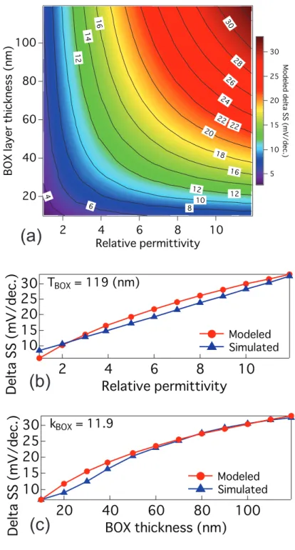
Fig. 2-6. Estimated enhanced SSs by the proposed model when T = 300 k and a = 2.5: (a) kBOX- and TBOX- related dependence, (b) kBOX-related dependence observed when TBOX is 119 nm along with that of the simulated result, and (c) TBOX-related dependence observed when kBOX is 11.9 along with that of the simulated result.
30
Figure 2-6 (a) shows the kBOX- and TBOX- related dependences of ΔSSM using parameter values in Table 2-1. The enhancement of SS estimated using the model as shown in Fig 2-6 (a) shows better agreement with that from the simulation shown in Fig. 2-5 (d). To compare these SSs in detail, the kBOX-related dependence seen when TBOX is 119 nm and the TBOX-related dependence seen when kBOX is 11.9 were evaluated using the model and using simulation, and the results are shown in Fig. 2-6 (b) and Fig. 2-6 (c), respectively. These figures demonstrate that the model appropriately reproduces the dependence of the increase of SSs on kBOX and TBOX, which indicates the enhancement of SSs are induced by the electric flux detouring from the drain through the BOX.
2.4 Summary
In this study, electric flux in dielectric regions of electron devices was quantitatively examined using stream functions for the first time ever. Electric flux lines intersecting equipotential lines normally were accurately visualized with a density proportional to the amount of electric flux. This allowed investigation of the kBOX- and TBOX-related dependences of electric flux detouring from the drain to the body region via the BOX layer, DIBL at the SOI/BOX interface and SSs. The simulation results indicated that detouring electric flux causes DIBL at the SOI/BOX interface and that DIBL enhances SS in SOI MOSFETs. The relationships linking flux, DIBL and SSs were also confirmed for SOI MOSFETs with GP structures. A compact model based on the flux for the enhanced SSs in SOI MOSFETs with such structures was also proposed, and produced SSs showing good agreement with simulated values. This agreement of SSs confirms that the enhancements of SSs in short channel SOI MOSFETs are induced by the drain electric flux detouring through the BOX. The findings of this study are expected to be useful in design of SOI MOSFETs and advanced SOQ, SOS and SON MOSFETs.
To improve the usability of the findings in this chapter, the compact model of the flux is evaluated in the next chapter.
31
References
[1] J.-P. Colinge, “Subthreshold slope of thin-film SOI MOSFET’s,” IEEE
Electron Device Letters, vol. 7, no. 4, pp. 244–246, Apr. 1986.
[2] J.-P. Colinge, Silicon-on-Insulator Technology: Materials to VLSI, 2nd ed. Boston: Kluwer, 2004, p. 384.
[3] A. Khakifirooz, K. Cheng, A. Reznicek, T. Adam, N. Loubet, H. He, J. Kuss, J. Li, P. Kulkarni, S. Ponoth, R. Sreenivasan, Q. Liu, B. Doris, and G. Shahidi, “Scalability of Extremely Thin SOI (ETSOI) MOSFETs to Sub-20-nm Gate Length,” IEEE Electron Device Letters, vol. 33, no. 2, pp. 149–151, Feb. 2012.
[4] M. B. Kleiner, S. A. Kuhn, and W. Weber, “Thermal conductivity measurements of thin silicon dioxide films in integrated circuits,” IEEE
Transactions on Electron Devices, vol. 43, no. 9, pp. 1602–1609, 1996.
[5] M. Jagadesh Kumar and A. A. Orouji, “Investigation of a new modified source/drain for diminished self-heating effects in nanoscale MOSFETs using computer simulation,” Physica E: Low-dimensional Systems and
Nanostructures, vol. 33, no. 1, pp. 134–138, Jun. 2006.
[6] K. Kajiwara, Y. Nakajima, T. Hanajiri, T. Toyabe, and T. Sugano, “Characterization of Distribution of Trap States in Silicon-on-Insulator Layers by Front-Gate Characteristics in n-Channel SOI MOSFETs,” IEEE
Transactions on Electron Devices, vol. 55, no. 7, pp. 1702–1707, Jul. 2008.
[7] Y. Nakajima, T. Toda, T. Hanajiri, T. Toyabe, and T. Sugano, “In-depth profiling of electron trap states in silicon-on-insulator layers and local mechanical stress near the silicon-on-insulator/buried oxide interface in separation-by-implanted-oxygen wafers,” Journal of Applied Physics, vol. 108, no. 12, p. 124505, Dec. 2010.
[8] Y. Nakajima, Y. Watanabe, T. Hanajiri, T. Toyabe, and T. Sugano, “Local-Stress-Induced Trap States in SOI Layers With Different Levels of Roughness at SOI/BOX Interfaces,” IEEE Electron Device Letters, vol. 32, no. 3, pp. 237–239, Mar. 2011.
32
[9] T. Hanajiri, T. Toyabe, and T. Sugano, “Suppression of short channel effects by full inversion in deep sub-micron gate SOI MOSFETs,” Solid-State
Electronics, vol. 45, no. 12, pp. 2077–2081, Dec. 2001.
[10] T. Ernst, C. Tinella, C. Raynaud, and S. Cristoloveanu, “Fringing fields in sub-0.1 µm fully depleted SOI MOSFETs: optimization of the device architecture,” Solid-State Electronics, vol. 46, no. 3, pp. 373–378, Mar. 2002.
[11] C. Fenouillet-Beranger, T. Skotnicki, S. Monfray, N. Carriere, and F. Boeuf, “Requirements for ultra-thin-film devices and new materials for the CMOS roadmap,” Solid-State Electronics, vol. 48, no. 6, pp. 961–967, Jun. 2004. [12] P. C. Yeh and J. G. Fossum, “Physical subthreshold MOSFET modeling
applied to viable design of deep-submicrometer fully depleted SOI low-voltage CMOS technology,” IEEE Transactions on Electron Devices, vol. 42, no. 9, pp. 1605–1613, 1995.
[13] V. P. Trivedi and J. G. Fossum, “Nanoscale FD/SOI CMOS: thick or thin BOX?,” vol. 26, 2005.
[14] W.-Y. Lu and Y. Taur, “On the scaling limit of ultrathin SOI MOSFETs,”
IEEE Transactions on Electron Devices, vol. 53, no. 5, pp. 1137–1141, May
2006.
[15] T. Yamada, Y. Nakajima, T. Hanajiri, and T. Sugano, “Suppression of Drain-Induced Barrier Lowering in Silicon-on-Insulator MOSFETs Through Source/Drain Engineering for Low-Operating-Power System-on-Chip Applications,” IEEE Transactions on Electron Devices, vol. 60, no. 1, pp. 260–267, Jan. 2013.
[16] T. Hanajiri, M. Niizato, K. Aoto, T. Toyabe, Y. Nakajima, T. Morikawa, and T. Sugano, “Scaling rules for SOI MOSFETs operating in the fully inverted mode,” Solid-State Electronics, vol. 48, no. 10–11, pp. 1943–1946, Oct. 2004.
[17] S. Abe, Y. Miyazawa, Y. Nakajima, T. Hanajiri, T. Toyabe, and T. Sugano, “Suppression of DIBL in deca-nano SOI MOSFETs by controlling permittivity and thickness of BOX layers,” in 2009 10th International
Conference on Ultimate Integration of Silicon, 2009, pp. 329–332.
[18] T. Numata and S.-I. Takagi, “Device Design for Subthreshold Slope and Threshold Voltage Control in Sub-100-nm Fully Depleted SOI MOSFETs,”
33
IEEE Transactions on Electron Devices, vol. 51, no. 12, pp. 2161–2167, Dec.
2004.
[19] S. Burignat, D. Flandre, M. K. Md Arshad, V. Kilchytska, F. Andrieu, O. Faynot, and J.-P. Raskin, “Substrate impact on threshold voltage and subthreshold slope of sub-32nm ultra thin SOI MOSFETs with thin buried oxide and undoped channel,” Solid-State Electronics, vol. 54, no. 2, pp. 213– 219, Feb. 2010.
[20] C. Fenouillet-Beranger, S. Denorme, P. Perreau, C. Buj, O. Faynot, F. Andrieu, L. Tosti, S. Barnola, T. Salvetat, X. Garros, M. Cassé, F. Allain, N. Loubet, L. Pham-Nguyen, E. Deloffre, M. Gros-Jean, R. Beneyton, C. Laviron, M. Marin, C. Leyris, S. Haendler, F. Leverd, P. Gouraud, P. Scheiblin, L. Clement, R. Pantel, S. Deleonibus, and T. Skotnicki, “FDSOI devices with thin BOX and ground plane integration for 32nm node and below,” Solid-State Electronics, vol. 53, no. 7, pp. 730–734, Jul. 2009. [21] X. Luo, J. Fan, Y. Wang, T. Lei, M. Qiao, B. Zhang, and F. Udrea,
“Ultralow Specific On-Resistance High-Voltage SOI Lateral MOSFET,”
IEEE Electron Device Letters, vol. 32, no. 2, pp. 185–187, Feb. 2011.
[22] J.-C. Guo and C.-T. Yeh, “A New Three-Dimensional Capacitor Model for Accurate Simulation of Parasitic Capacitances in Nanoscale MOSFETs,”
IEEE Transactions on Electron Devices, vol. 56, no. 8, pp. 1598–1607, Aug.
2009.
[23] E. Palm and F. Van de Wiele, “Current lines and accurate contact current evaluation in 2-D numerical simulation of semiconductor devices,” IEEE
Transactions on Electron Devices, vol. 32, no. 10, pp. 2052–2059, Oct. 1985.
[24] M. S. Mock, “A two-dimensional mathematical model of the insulated-gate field-effect transistor,” Solid-State Electronics, vol. 16, no. 5, pp. 601–609, May 1973.
[25] “TCAD Sentaurus.” [Online].
Available:http://www.synopsys.com/Tools/TCAD/. [Accessed: 01-Sep-2013].
[26] M. Horstmann, M. Wiatr, A. Wei, J. Hoentschel, T. Feudel, T. Scheiper, R. Stephan, M. Gerhadt, S. Krügel, and M. Raab, “Advanced SOI CMOS transistor technology for high performance microprocessors,” Solid-State
34
[27] Z. Ren, M. Ieong, J. Cai, J. Holt, D. Boyd, R. Mo, H. Yin, O. Dokumaci, S. Kawanaka, T. Sato, P. Ronsheim, J. Wang, C. Y. Sung, and W. Haensch, “Selective epitaxial channel ground plane thin SOI CMOS devices,” in IEEE
InternationalElectron Devices Meeting, 2005. IEDM Technical Digest., 2005,
pp. 733–736.
[28] J. Borland, M. Tanjyo, S. Sakai, T. Nagayama, H. Kiyama, and K. Suguro, “Comparison of BF2, In, Ga, C+Ga & In+BF2 Dopant for 22nm node bulk & PD-SOI HALO implantation or ground plane back-gate doping for FD-SOI CMOS technologies,” in 2012 12th International Workshop on
Junction Technology, 2012, pp. 38–41.
[29] P. Kulkarni, Q. Liu, A. Khakifirooz, Y. Zhang, K. Cheng, F. Monsieur, and P. Oldiges, “Impact of substrate bias on GIDL for thin-BOX ETSOI devices,” in 2011 International Conference on Simulation of Semiconductor Processes
and Devices, 2011, pp. 103–106.
[30] C. Riddet, C. Alexander, A. R. Brown, S. Roy, and A. Asenov, “Simulation of ‘Ab Initio’ Quantum Confinement Scattering in UTB MOSFETs Using Three-Dimensional Ensemble Monte Carlo,” IEEE Transactions on Electron
Devices, vol. 58, no. 3, pp. 600–608, Mar. 2011.
[31] A. Wettstein, A. Schenk, and W. Fichtner, “Quantum device-simulation with the density-gradient model on unstructured grids,” IEEE Transactions on
Electron Devices, vol. 48, no. 2, pp. 279–284, 2001.
[32] “ITRS Reports.” [Online]. Available: http://www.itrs.net/reports.html. [Accessed: 01-Sep-2013].
[33] Y. Nakajima, K. Sasaki, T. Hanajiri, T. Toyabe, and T. Sugano, “Drive Current Enhancement in Silicon-on-Quartz MOSFETs,” IEEE Electron
Device Letters, vol. 29, no. 8, pp. 944–945, Aug. 2008.
[34] S. G. Nassif-Khalil and C. A. T. Salama, “Super-junction LDMOST on a silicon-on-sapphire substrate,” IEEE Transactions on Electron Devices, vol. 50, no. 5, pp. 1385–1391, May 2003.
[35] J. Widiez, M. Rabarot, S. Saada, J.-P. Mazellier, J. Dechamp, V. Delaye, J.-C. Roussin, F. Andrieu, O. Faynot, S. Deleonibus, P. Bergonzo, and L. Clavelier, “Fabrication of Silicon on Diamond (SOD) substrates by either the Bonded and Etched-back SOI (BESOI) or the Smart-CutTM technology,”
35
[36] C. Durand, F. Casset, P. Renaux, N. Abele, B. Legrand, D. Renaud, E. Ollier, P. Ancey, A. M. Ionescu, and L. Buchaillot, “In-Plane Silicon-On-Nothing Nanometer-Scale Resonant Suspended Gate MOSFET for In-IC Integration Perspectives,” IEEE Electron Device Letters, vol. 29, no. 5, pp. 494–496, May 2008.
36
Chapter 3. A
Modeling of Drain Electric Flux
Passing through the BOX layer in Subthreshold
Regions of SOI MOSFETs with Ground Plane
Structures
37
3.1 Introduction
In the previous chapter, I extracted amounts of electric flux via BOX layers, and discussed its effects on MOSFET characteristics. In this chapter, I develop a model of this flux.
Silicon on insulator (SOI) technology contributes significantly to MOSFET scaling, which is essential in improving the electrical performance of very-large-scale integration (VLSI). Related advantages over conventional bulk technology owing to the use of buried-oxide (BOX) layers include low junction capacitance, minimal leakage current, high gate controllability, high robust breakdown voltage and high radiation hardness [1]–[3]. However, BOX layers are also associated with the disadvantages of low thermal conductivity [4], [5], trap generation at the SOI/BOX interface [6], [7] and leakage current enhanced by drain-induced barrier lowering (DIBL) [8]–[17]. This BOX layer-related DIBL originates from electric flux or electric field detouring from the drain to the body region via the BOX layer [8]–[17] as mentioned in previous chapter. However, the amount of flux involved has not yet been clarified, and modeling for clarification has also been minimal. Some reports have addressed the use of conformal mapping techniques to model MOSFET electrical parameters such as parasitic capacitance, potential, subthreshold current and electric field, and these can be classified into several types based on conformal mapping shapes as detailed below.
Figure 3-1 (a) shows conformal mapping on two boundaries with an angle of 90 degrees between them and mapping for side-wall analysis [18]–[20]. Figure 3-1 (b) shows L-shaped conformal mapping regions used for analysis of parameters such as gate/drain parasitic capacitance [21], [22]. Figure 3-1 (c) shows a box-shaped conformal mapping region used for analysis of electrical characteristics in double-gate MOSFETs [23]–[25]. Figure 3-1 (d) shows a U-shaped conformal mapping region used for analysis of electrical characteristics in planar or fin FETs [26]–[29]. Figure 3-1 (e) shows conformal mapping using boundaries along a straight line as used for analysis of fringe capacitance [30]. Figure 3-1 (f) shows conformal mapping using boundaries along two parallel lines
38
as used for analysis of fringe capacitance in the BOX layer [10], [31]. However, these previous studies included little analysis of BOX layer-related characteristics, and the parameters of both the BOX layer and the SOI layer were not considered together. Against such a background, this study involved the investigation of a model of drain electric flux detouring through the BOX layer in the subthreshold region of ground-plane (GP) [32]–[34] SOI MOSFETs. The model involves a unique conformal mapping shape (Fig. 3-1 (g)) that provides advantages over the approaches reported in previous papers, including consideration for the parameters of both the BOX and SOI layers at the same time. The model can be set with different permittivity levels for each layer to support such simultaneous consideration, making it applicable not only to SOI MOSFETs but also to other MOSFETs on insulators with various permittivity levels, including silicon-on-sapphire (SOS) [35], [36], silicon-on-diamond (SOD) [37] and silicon-on-nothing (SON) [38] types.
Fig. 3-1. Shapes of conformal mappings in (a–f) previous studies and (g) this study.
39
3.2 Modeling
A typical path of electric flux passing from the drain to the body via the BOX layer in the subthreshold region of a GP SOI MOSFET is shown in Fig. 2, and the amount of such detouring flux was modeled in this study. When the device operates in the saturation region, electric flux is terminated to numerous carriers in the body region. In contrast, when the device operates in the subthreshold region, there are few carriers in the body region and most of the flux directly reaches the gate to which a low voltage is applied. Accordingly, the amount of the flux passing from the drain to the body in this study was assumed to be the same as that from the drain to the gate. The model was used to estimate this amount passing via not only the BOX layer but also via the SOI and gate oxide layers based on the stream function [39], [40] derived from conformal mapping.
Fig. 3-2. Typical cross-sectional view of a SOI MOSFET in potential distribution and electric flux when strong flux passing from the drain to the body region via the BOX layer is detected. Electric flux is shown with solid lines in the BOX layer, and the flux passing from the drain to the body is highlighted by the open ellipse.
40
3.2.1 Approximation for modeling
To model drain electric flux amounts in SOI MOSFETs using conformal mapping as shown in Fig. 3-3 (a), three approximations are applied to MOSFETs: 1) the charge in the SOI layer is ignored, 2) there is homogenization of permittivity in the whole analysis region, and 3) the source region is ignored and the electrode shape is simplified. 1) and 2) are necessary to approximate Poisson’s equation as Laplace’s equation , which can be solved analytically using the conformal mapping. 3) is an approximation to simplify the shape of the mapping, and as a result, the gate, drain and substrate boundaries are taken into consideration in the model. The final approximated structure and these boundaries are summarized in Fig. 3-3 (b). In particular, the approximation in 2) is realized by varying the effective thickness of the layer depending on permittivity.
ε!"#$#%&' → ε!""#$%&!, (A.1) ∆y!"#$#%&' → ∆y!""!#$%&!, (A.2) ∆y!""!#$%&!≡ !!""#$%&!
!!"#$#%&'∙ ∆y!"#$#%&', (A.3)
where ε!"#$#%&' is the level of permittivity before approximation, ε!""#$%&! is that after approximation, ∆y!"#$#%&' is the thickness before approximation, and ∆y!""!#$%&! is that after approximation. The pre- and post-approximation generated capacitances C!"#$#%&' and C!""#$%&! in the layer are kept constant.
C!"#$#%&' =∆!!"#$#%&' !!"#$#%&', (A.4) C!""#$%&! =∆!!""#$%&! !!""#$%&! = ∆!!"#$#%&' !!"#$#%&' . (A.5)
41
The permittivity of the SOI layer ε!"# is set as per the permittivity in the BOX layer ε!"#, and the original SOI thickness T!"# is converted to the effective SOI thickness T!"#$ using these permittivity values.
ε!"# → ε!"#, (A.6)
T!"#$ =!!"#
!!"# ∙ T!"#. (A.7)
The permittivity of the gate oxide ε!"# is set to ε!"#, and the effective gate oxide thickness is also converted using the original gate oxide thickness T!"#
T!"#$ →!!"#
!!"#∙ T!"#. (A.8)
These approximations become valid when the following conditions are met in the SOI MOSFET: 1) operation takes place in subthreshold regions, where the charge in the body is negligible, 2) ε!"# is close to ε!"# because the error caused by the approximation of T!"# to T!"#$ is large when the difference between ε!"# and ε!"# is large, 3) the ratio of the BOX thickness T!"# to T!"# is large enough to allow the effect of the drain/body interface to be ignored, and 4) the gate length LG is large enough to allow the source region to be ignored.
Fig. 3-3. Schematic views of SOI MOSFETs (a) before approximation and (b) after approximation with boundaries considered. The boundaries are shown by thick lines.
42
3.2.2 Electric flux analysis using conformal mapping
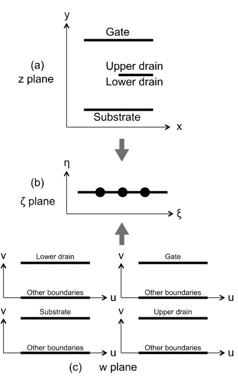
The potential and the related stream function of Laplace’s equation in Cartesian coordinates can be derived analytically using conformal mapping. To perform such mapping, the x and y coordinates of complicated boundaries in the analyzed region are assigned to real and imaginary parts of the complex number z, respectively, as shown in Fig. 3-4 (a), and the stream function u and the potential v in simple boundaries are assigned to real and imaginary parts of the complex number w, respectively, as shown in Fig. 3-4 (c). These complex numbers are associated with the complex parameter ζ, which has a real part ξ and an imaginary part η as shown in Fig. 3-4 (b), and the assignment between z and ζ and w and ζ is derived via conformal mapping. In this study, four boundaries (for the gate, upper drain, lower drain and substrate) were considered as shown in Fig. 3-4 (a), and for each boundary, a w plane can be defined as shown in Fig. 3-4 (c).
In each w plane for each boundary, the stream function and potential are derived from the applied voltage individually, and in order to model the drain electric flux, the w plane for lower drain is required.
43
Fig. 3-4. Schematic views of complex planes in (a) the z plane, (b) the ζ plane, and (c) the w plane.
44
3.2.3 Relationship between the z and ζ planes
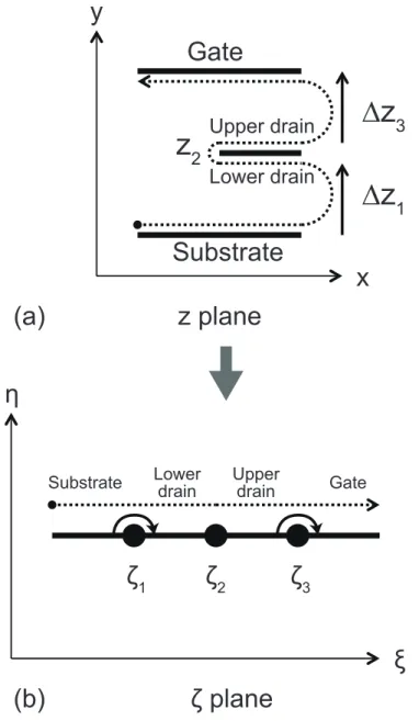
Schematic views of the z and ζ planes are shown in Fig. 3-5. To derive the relationship between them, dz dζ formulated using Schwarz-Christoffel transformations [29], [31] as follows: !" !"= a!∙ ζ − ζ! !!!! ∙ ζ − ζ ! ! !! ! ∙ ζ − ζ! ! !! ! = a!∙ !!!! !!!! ∙ !!!! (C.1)
where a! is a proportionality coefficient and z is formulated using partial fraction
decomposition as follows: z = !"!!∙ dζ = !! !!!!!∙ !!!!! !!!! + !!!!! !!!! ∙ dζ = !! !!!!!∙ ζ!− ζ! ∙ ln ζ − ζ! + ζ!− ζ! ∙ ln ζ − ζ! +b! (C.2)
where b! is a constant of integration. The ∆z! and ∆z! shown in Fig. 3-5 (a) are derived using Cauchy's integral formula as follows:
∆z! = −!!∙ ! !"!!∙ dζ ! = − ! !∙ !!∙!!!!!!!! !!!! ∙ dζ !! = −i ∙ π ∙ a!∙!!!!!! !!!!, (C.3) ∆z! = −!!∙ ! !!"!!∙ dζ= −!!∙ !!∙!!!!!!!! !!!! ∙ dζ !!