Digital Compensation Schemes for Signal Distortion in OFDM Receivers
July 2009
Mamiko Inamori
DISSERTATION
Submitted to the School of Integrated Design Engineering, Keio University, in partial fulfillment of the requirements for the degree
of Doctor of Philosophy
Abstract
Various wireless standards have been developed for realizing broadband anywhere / anytime access network. Orthogonal division frequency multiplexing (OFDM) is currently a dominant modulation scheme in broadband wireless systems. The receiver is required to satisfy the conditions such as high-performance, low power consumption, small size, and low cost. However, in the receiver for the broadband signal, more accuracy of analog components is necessary and it leads to larger cost and power consumption. To implement a low cost and low power consumption receiver, compensation of the signal distortion in a digital domain is required. The signal distortion compensation in the digital domain brings more scalability and flexibility. In this dissertation, digital signal compensation schemes for the signal distortion due to radio frequency (RF) components, timing jitter, and baseband filter in OFDM receivers are proposed and investigated.
Chapter 1 introduces the background of the OFDM receivers and the motivation of the research.
In Chapter 2, compensation schemes for signal distortion in a direct conversion receiver are investigated. The OFDM direct conversion receiver is superior to a superheterodyne receiver in cost, size, and power consumption. However, this receiver architecture suffers from DC offset, frequency offset, and IQ imbalance.
In the proposed scheme, the key idea is to use a differential filter for the reduction of the DC offset. From the outputs of differential filter in the training sequence, the frequency offset is estimated with auto-correlation in the presence of DC offset.
The proposed scheme shows better estimation accuracy of the frequency offset than
the conventional scheme with a high pass filter. The IQ imbalance is calculated in
time domain using a simple equation without the impulse response of a channel
in the presence of the frequency offset and the DC offset. However, the accuracy
of the IQ imbalance estimation with the proposed scheme in the time domain
is deteriorated when the frequency offset is small. To overcome this problem,
frequency domain IQ imbalance estimation scheme is also proposed, which uses the
pilot subcarriers in the data period. Numerical results obtained through computer
simulation show that estimation accuracy and bit error rate (BER) performance can be improved even if the frequency offset is small. Thus, the combination of two low-complexity IQ imbalance estimation schemes is suitable for low-cost and low-power-consumption direct conversion receivers.
In Chapter 3, signal distortion caused by timing jitter is discussed. As one of new receiver architectures, a RF-sampling receiver has been proposed, which directly processes analog discrete samples. In this architecture, a phase locked loop (PLL) exhibits the phase noise and then causes the timing jitter. In wireless receivers, quadrature sampling is required in order to demodulate I-phase and Q- phase signals. Different from simple charge sampling, timing jitter causes crosstalk between these signals. In Chapter 3, the effect of the timing jitter on quadrature sampling in the RF-sampling receiver is analyzed.
In Chapter 4, compensation schemes for signal distortion in fractional sampling (FS) OFDM receivers are evaluated. The OFDM system with FS can achieve diversity with a single antenna. However, as the number of subcarriers and the oversampling ratio increase, the correlation among the noise components over dif- ferent subcarriers deteriorates the BER performance. First, a correlated noise cancellation scheme in FS orthogonal frequency and code division multiplexing (OFCDM) system is investigated. To reduce the correlated noise, an alternative spreading code (ASC) is used in the FS OFCDM system. This spreading code has positive and negative components alternatively. Despreading with the ASC can- cels most of the correlated noise components. However, this alternative spreading code reduces the number of available spreading codes. For applicability to OFDM systems, the effect of the correlation among the noise components in FS OFDM system is derived. A metric weighting scheme for the coded FS OFDM system is also proposed and investigated.
Chapter 5 summarizes the results of each chapter and concludes this disserta-
tion.
Contents
Abstract iii
List of Acronyms xix
List of Notations xxiii
1 General Introduction 1
1.1 Broadband Wireless System . . . . 1
1.1.1 Broadband Cellular System . . . . 1
1.1.2 Broadband Wireless Access Network . . . . 3
1.1.2.1 WPAN . . . . 4
1.1.2.2 WLAN . . . . 5
1.1.2.3 WMAN . . . . 6
1.1.2.4 WWAN . . . . 6
1.2 OFDM Receiver . . . . 6
1.3 OFDM Receiver Architecture . . . . 8
1.3.1 Superheterodyne Receiver . . . . 8
1.3.2 Direct Conversion Receiver . . . . 9
1.3.3 RF-sampling Receiver . . . . 11
1.3.4 Fractional Sampling . . . . 12
1.4 Signal Distortion in OFDM Receivers . . . . 15
1.4.1 Distortion due to RF Components . . . . 15
1.4.2 Distortion due to PLL . . . . 17
1.4.3 Distortion due to Baseband Filter . . . . 18
1.5 Motivation of this Research . . . . 22
1.6 References . . . . 27
2 Frequency Offset and IQ Imbalance Estimation Scheme in the
Presence of Time-varying DC offset for Direct Conversion Re-
ceivers 35
2.1 Frequency Offset Estimation Scheme in the Presence of Time-varying
DC Offset for Direct Conversion Receivers . . . . 36
2.1.1 Introduction . . . . 36
2.1.2 System Model . . . . 38
2.1.2.1 Preamble Model . . . . 38
2.1.2.2 Subcarrier Allocation . . . . 39
2.1.2.3 RF Architecture and Automatic Gain Control . . . 39
2.1.3 Frequency Offset Estimation . . . . 40
2.1.3.1 Coarse Estimation and Fine Estimation . . . . 40
2.1.3.2 Conventional Scheme . . . . 40
2.1.3.3 Proposed Scheme . . . . 41
2.1.3.4 Time-varying DC Offset . . . . 43
2.1.4 Numerical Results . . . . 45
2.1.4.1 Simulation Conditions . . . . 45
2.1.4.2 MSE vs. Threshold Level Under Time-varying DC Offset . . . . 46
2.1.4.3 MSE of Frequency Estimation Under Time-varying DC Offset . . . . 48
2.1.4.4 MSE vs. Threshold Level Under Constant DC Offset 48 2.1.4.5 MSE under Various Received Signal Power . . . . . 50
2.1.5 Conclusions . . . . 50
2.2 Performance Analysis of Frequency Offset Estimation in the Pres- ence of IQ Imbalance for OFDM Direct Conversion Receivers with Differential Filter . . . . 50
2.2.1 Introduction . . . . 51
2.2.2 System Model . . . . 51
2.2.3 Analysis of Frequency Offset Estimation . . . . 52
2.2.3.1 Frequency Offset Estimation with Differential Filter 52 2.2.3.2 MSE Performance . . . . 54
2.2.4 Numerical Results . . . . 57
2.2.4.1 Simulation Conditions . . . . 57
2.2.4.2 MSE Performance of Frequency Offset Estimation under IQ imbalance . . . . 58
2.2.5 Conclusions . . . . 60
2.3 Time Domain IQ Imbalance Estimation Scheme in the Presence of Frequency Offset and Time-varying DC Offset for Direct Conversion
Receivers . . . . 61
2.3.1 Introduction . . . . 61
2.3.2 System Model . . . . 62
2.3.3 Frequency Offset Estimation . . . . 64
2.3.3.1 Frequency Offset, DC Offset, and IQ Imbalance Model . . . . 64
2.3.3.2 Frequency Offset Estimation Using Differential Filter 65 2.3.4 IQ Imbalance Estimation . . . . 66
2.3.4.1 IQ Imbalance Estimation . . . . 66
2.3.4.2 IQ Imbalance Compensation . . . . 68
2.3.5 Simulation Results . . . . 69
2.3.5.1 Simulation Conditions . . . . 69
2.3.5.2 Normalized MSE Performance of Phase Mismatch Estimation vs. Phase Mismatch . . . . 70
2.3.5.3 Normalized MSE Performance of Phase Mismatch Estimation vs. Frequency Offset . . . . 71
2.3.5.4 Normalized MSE Performance of Gain Mismatch Estimation . . . . 72
2.3.5.5 BER Performance . . . . 72
2.3.6 Conclusions . . . . 74
2.4 Frequency Domain IQ Imbalance Estimation Scheme in the Presence of DC Offset and Frequency Offset . . . . 74
2.4.1 Introduction . . . . 74
2.4.2 System Model . . . . 75
2.4.3 Frequency Offset Estimation Using Differential Filter . . . . 76
2.4.4 Proposed IQ Imbalance Estimation . . . . 77
2.4.4.1 Influence of Differential Filter . . . . 77
2.4.4.2 IQ Imbalance Estimation without Frequency Offset 77 2.4.4.3 IQ imbalance Estimation in the presence of Fre- quency Offset . . . . 79
2.4.5 Simulation Results . . . . 81
2.4.5.1 Simulation Conditions . . . . 81
2.4.5.2 Normalized MSE Performance vs. Frequency Offset 81
2.4.5.3 Normalized MSE Performance vs. Gain Mismatch
and Phase Mismatch . . . . 83
2.4.5.4 BER Performance vs. Frequency Offset . . . . 86
2.4.5.5 BER Performance vs. E
b/N
0. . . . 87
2.4.6 Conclusions . . . . 88
2.5 Conclusions of Chapter 2 . . . . 88
2.6 References . . . . 88
3 Effect of Timing Jitter on Quadrature Charge Sampling 93 3.1 Introduction . . . . 93
3.2 System Model . . . . 94
3.2.1 Receiver Architecture . . . . 94
3.2.2 Charge Sampling Circuit . . . . 95
3.2.3 PLL Model . . . . 95
3.3 Numerical Analysis . . . . 97
3.3.1 Single Carrier QAM . . . . 97
3.3.2 OFDM Modulation . . . 101
3.3.3 SNR and SINR . . . 101
3.3.4 Comparison of Charge Sampling and Voltage Sampling . . . 102
3.4 Numerical Results . . . 103
3.4.1 Simulation Conditions . . . 103
3.4.2 SNR and SINR . . . 104
3.4.3 BER . . . 105
3.5 Conclusions of Chapter 3 . . . 106
3.6 References . . . 107
4 Correlated Noise Cancellation Scheme in Fractional Sampling OFDM System 111 4.1 Fractional Sampling OFCDM with Alternative Spreading Code . . . 111
4.1.1 Introduction . . . 112
4.1.2 System Model . . . 112
4.1.2.1 Transmitter Model . . . 112
4.1.2.2 Receiver Structure with Fractional Sampling . . . . 113
4.1.3 Proposed Scheme . . . 114
4.1.3.1 Despreading with Non-alternative Spreading Code 114 4.1.3.2 Despreading with Alternative Spreading Code . . . 116
4.1.4 Numerical Results . . . 116
4.1.4.1 Simulation Conditions . . . 116
4.1.4.2 BER Improvement with Alternative Spreading Code117
4.1.4.3 Number of Subcarriers . . . 118
4.1.4.4 Spreading Factor S
f. . . 119
4.1.4.5 Spreading Code . . . 121
4.1.5 Conclusions . . . 122
4.2 Effect of Pulse Shaping Filters on a Fractional Sampling OFDM System with Subcarrier-Based Maximal Ratio Combining . . . 122
4.2.1 Introduction . . . 125
4.2.2 Receiver Structure with Fractional Sampling . . . 126
4.2.3 Noise Correlation among Samples . . . 126
4.2.4 Numerical Results . . . 128
4.2.4.1 Simulation Conditions . . . 128
4.2.4.2 Channel Models . . . 129
4.2.4.3 Pulse Shaping Filters . . . 131
4.2.4.4 Frequency Spectrum of the Filter and Frobenius Norm of the Whitening Matrix . . . 132
4.2.4.5 Uncoded FS OFDM . . . 134
4.2.4.6 Coded FS OFDM . . . 141
4.2.5 Conclusions . . . 144
4.3 Conclusions of Chapter 4 . . . 144
4.4 References . . . 145
5 Overall Conclusions 147 5.1 Signal Compensation Schemes in OFDM Direct Conversion Receivers147 5.2 Signal Compensation Schemes in RF-sampling Receivers . . . 148
5.3 Signal Compensation Schemes in FS OFDM Receivers . . . 149
Acknowledgements 151
List of Achievements 153
List of Figures
1.1 Wireless standard. . . . . 3
1.2 IEEE 802 standard. . . . 5
1.3 OFDM transmitter architecture. . . . 7
1.4 OFDM receiver architecture. . . . 8
1.5 Evolution of receiver architectures. . . . 8
1.6 Superheterodyne receiver architecture. . . . 9
1.7 Downconversion in superheterodyne receiver. . . . 9
1.8 Direct conversion receiver architecture. . . . 10
1.9 Downconversion in direct conversion receiver. . . . . 10
1.10 DC offset and frequency offset. . . . 11
1.11 IQ imbalance model. . . . 12
1.12 RF sampling receiver architecture. . . . 13
1.13 Downconversion in RF sampling receiver. . . . 13
1.14 Influence of timing jitter. . . . 14
1.15 Influence of timing jitter. . . . 15
1.16 Fractional sampling receiver. . . . 15
1.17 Fractional sampling in delay domain. . . . 16
1.18 Correlation between noise components. . . . 22
1.19 Overall structure of this research. . . . 23
1.20 Relationship of this research. . . . 24
1.21 Overall model about distortion due to RF components. . . . 27
1.22 Overall model about distortion due to PLL. . . . 28
1.23 Overall model about distortion due to baseband filters. . . . 28
2.1 OFDM direct conversion architecture. . . . 37
2.2 IEEE 802.11a/g burst structure. . . . 38
2.3 Subcarriers allocation. . . . 38
2.4 Receiver architecture. . . . 39
2.5 Effect of DC offset in conventional scheme. . . . 41
2.6 Overall system model. . . . 42
2.7 DC offset and the output of differential filter. . . . . 44
2.8 LO leakage. . . . 46
2.9 MSE vs. threshold level performance of frequency offset estimation (cutoff freq.=1[kHz], E
b/N
0=15[dB]). . . . 46
2.10 MSE vs. threshold level performance of frequency offset estimation (cutoff freq.=10[kHz], E
b/N
0=15[dB]). . . . . 47
2.11 MSE vs. threshold level performance of frequency offset estimation (cutoff freq.=100[kHz], E
b/N
0=15[dB]). . . . 47
2.12 MSE performance of frequency offset estimation under time-varying DC offset (coarse+fine, cutoff freq.=10[kHz]). . . . . 48
2.13 MSE performance of frequency offset estimation under constant DC offset (coarse+fine, cutoff freq.=10[kHz]). . . . 49
2.14 MSE vs. received signal power (E
b/N
0=15[dB], cutoff freq.=10[kHz]). 49 2.15 Receiver architecture. . . . 52
2.16 Vectors representation of auto-correlation. . . . 55
2.17 Cancelation in auto-correlation. . . . 56
2.18 MSE vs. SNR (β=0.05, θ=5[degrees]). . . . 58
2.19 MSE vs. normalized frequency offset (θ=5[degrees], β=0.05). . . . . 59
2.20 MSE vs. gain mismatch (normalized freq. offset=0.3, θ=5[degrees]). 60 2.21 MSE vs. phase mismatch (normalized freq. offset=0.3, β=0.05). . . 60
2.22 DC offset and the output of differential filter. . . . . 63
2.23 Receiver architecture. . . . 64
2.24 Normalized MSE performance of phase mismatch estimation vs. phase mismatch (β=0.05, normalized freq. offset = 0.3). . . . 70
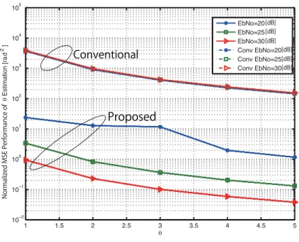
2.25 Normalized MSE performance of phase mismatch estimation vs. fre- quency offset (β=0.05, θ= 5[degrees]). . . . . 71
2.26 Normalized MSE performance of gain mismatch estimation (θ= 5[degrees], normalized freq. offset=0.3). . . . 72
2.27 BER performance with 1st order interpolation (normalized freq. off- set=0.3, β=0.05, θ=5[degrees]). . . . 73
2.28 Subcarrier frequency allocation. . . . 75
2.29 Vector representation of pilot subcarriers with IQ imbalance. . . . . 78
2.30 Receiver architecture of proposed scheme. . . . . 80
2.31 Effect of ICI and frequency offset. . . . 81
2.32 Normalized MSE performance of gain mismatch estimation (β=0.05,
θ=5[degrees]). . . . 82
2.33 Normalized MSE performance of phase mismatch estimation (β=0.05, θ=5[degrees]). . . . 83
2.34 Real part of the second term of Eq. (2.80) (SNR = ∞ , β=0.05, θ=5[degrees]). . . . 84
2.35 Imaginary part of the second term of Eq. (2.80) (SNR = ∞ , β=0.05, θ=5[degrees]). . . . 84
2.36 Normalized MSE performance of gain mismatch estimation (α=0.001, θ=5[degrees]). . . . 85
2.37 Normalized MSE performance of phase mismatch estimation (α=0.001, β=0.05). . . . 85
2.38 BER vs. normalized frequency offset α (64QAM, β=0.05, θ=5[degrees]). 86 2.39 BER vs. E
b/N
0(64QAM, β =0.05, θ=5[degrees]). . . . 87
3.1 Block diagram of the receiver. . . . 95
3.2 Simple integrating charge sampling circuit. . . . 95
3.3 Block diagram of the PLL. . . . 96
3.4 Typical PSD of the PLL phase noise. . . . 96
3.5 Modeled PSD of the PLL phase noise. . . . . 97
3.6 Quadrature sampling. . . . 98
3.7 Sampling of the I-phase component. . . . 99
3.8 SNR and SINR versus symbol rate, (single carrier, E
b/N
0= 14 [dB]).105 3.9 SNR and SINR versus symbol rate, (OFDM, E
b/N
0= 14 [dB]). . . 106
3.10 BER versus Eb/No, (N
g=-100 [dBc/Hz], symbol rate=100 [Msym- bol/s], single carrier 64QAM). . . 106
3.11 BER versus symbol rate (N
g= -100 [dBc/Hz], E
b/N
0= 14 [dB], single carrier 64QAM). . . 107
4.1 OFCDM transmitter block diagram. . . 113
4.2 Receiver block diagram. . . . 113
4.3 Correlation of the noise components (logarithmic representation of absolute value). . . 114
4.4 PSD vs. normalized frequency with different pulse shapes. . . 118
4.5 Multipath channel models. . . 119 4.6 BER performance vs. E
b/N
0on the 16 path Rayleigh fading channel
with the uniform delay profile (number of subcarriers: 1024, S
f=2). 120
4.7 BER performance vs. E
b/N
0on the 24 path Rayleigh fading channel with the exponential delay profile (number of subcarriers: 1024,
S
f=2). . . 121
4.8 BER performance vs. number of subcarriers on the 16 path Rayleigh fading channel with the uniform delay profile (S
f= 2, E
b/N
0= 15[dB]). . . 122
4.9 BER performance vs. number of subcarriers on the 24 path Rayleigh fading channel with the exponential delay profile (S
f= 2, E
b/N
0= 15[dB]). . . 123
4.10 BER performance vs. spreading factor S
fon the 16 path Rayleigh fading channel with the uniform delay profile (number of subcarri- ers:1024, E
b/N
0= 15[dB]). . . 123
4.11 BER performance vs. spreading factor S
fon the 24 path Rayleigh fading channel with the exponential delay profile (number of sub- carriers:1024, E
b/N
0= 15[dB]). . . 124
4.12 BER performance vs. G with different spreading codes on the 16 path Rayleigh fading channel with the uniform delay profile (number of subcarriers:1024, E
b/N
0= 15[dB]). . . 124
4.13 BER performance vs. G with different spreading codes on the 24 path Rayleigh fading channel with the exponential delay profile (number of subcarriers:1024, E
b/N
0= 15[dB]). . . 125
4.14 Block diagram of a receiver. . . 126
4.15 Correlation of the noise components (logarithm representation of absolute value). . . 127
4.16 6-ray GSM Typical Urban model. . . 129
4.17 Multipath Rayleigh fading channel models. . . 130
4.18 Graphical illustration of the pulse shaping filters. . . 131
4.19 Frobenius norm of the whitening filter for different impulse responses (Number of subcarriers=64, G = 2). . . . 133
4.20 Frobenius norm of the whitening filter for different impulse responses (Number of subcarriers=64, G = 4). . . . 133
4.21 Frobenius norm of the whitening filter for different impulse responses (Number of subcarriers=1024, G = 4). . . 134
4.22 BER performance vs. E
b/N
0on the 16 path Rayleigh fading channel
with the uniform delay profile (QPSK, Number of subcarriers=64,
G = 1). . . . 135
4.23 BER performance vs. E
b/N
0on the 16 path Rayleigh fading channel with the uniform delay profile (QPSK, Number of subcarriers=64, G = 2). . . . 135 4.24 BER performance vs. E
b/N
0on the 16 path Rayleigh fading channel
with the uniform delay profile (QPSK, Number of subcarriers=64, G = 4). . . . 136 4.25 BER performance vs. E
b/N
0on the 16 path Rayleigh fading channel
with the uniform delay profile (16QAM, Number of subcarriers=64, G = 4). . . . 136 4.26 BER performance vs. E
b/N
0on the 16 path Rayleigh fading channel
with the uniform delay profile (64QAM, Number of subcarriers=64, G = 4). . . . 137 4.27 BER performance vs. E
b/N
0on the 16 path Rayleigh fading channel
with the uniform delay profile (QPSK, Number of subcarriers=1024, G = 4). . . . 138 4.28 BER performance vs. E
b/N
0on the 16 path Rayleigh fading chan-
nel with the uniform delay profile (16QAM, Number of subcarri- ers=1024, G = 4). . . 138 4.29 BER performance vs. E
b/N
0on the 16 path Rayleigh fading chan-
nel with the uniform delay profile (64QAM, Number of subcarri- ers=1024, G = 4). . . 139 4.30 BER performance vs. E
b/N
0on the 24 path Rayleigh fading chan-
nel with the exponential delay profile (QPSK, Number of subcarri- ers=1024, G = 4). . . 139 4.31 BER performance vs. E
b/N
0on the GSM Typical Urban model
(QPSK, Number of subcarriers=1024,G = 4). . . . 140 4.32 BER performance vs. E
b/N
0of coded OFDM (QPSK, Number of
subcarriers=64, G = 4). . . . 142 4.33 BER performance vs. E
b/N
0of coded OFDM with Adjusted Metric
(QPSK, Number of subcarriers=64, G = 4). . . 142 4.34 BER performance vs. E
b/N
0of coded OFDM (QPSK, Number of
subcarriers=1024, G = 4). . . 143 4.35 BER performance vs. E
b/N
0of coded OFDM with Adjusted Metric
(QPSK, Number of subcarriers=1024, G = 4). . . 143
List of Tables
1.1 Cellular systems. . . . 4
1.2 IEEE 802.11 protocols. . . . 7
1.3 Outline of the proposed approaches. . . . 29
2.1 Simulation conditions. . . . 45
2.2 Simulation conditions. . . . 58
2.3 Simulation conditions. . . . 69
2.4 Pilot subcarriers. . . . 77
2.5 Simulation conditions. . . . 82
3.1 Simulation conditions. . . 104
4.1 Simulation conditions. . . 117
4.2 Spreading code. . . 120
4.3 Simulation conditions . . . 128
4.4 6-ray GSM Typical Urban model parameters. . . . 129
List of Acronyms
1G first generation 2G second generation 3G third generation
3GPP third generation partnership project 3GPP2 third generation partnership project 2 3.9G 3.9 generation
4G fourth generation
64QAM quadrature amplitude modulation A/D analog-to-digital
ADC analog-to-digital converter AGC automatic gain control AFC automatic frequency control AWGN additive white Gaussian noise BER bit error rate
BPF band pass filter
CDMA code division multiple access
CMOS complementary metal oxide semiconductor DC direct current
DFT discrete Fourier transform
DS/SS direct sequence / spread-spectrum FCC federal communications commission FDMA frequency division multiple access FIR finite impulse response
FS fractional sampling GI guard interval HPF high pass filter
HSDPA High Speed Downlink Packet Access I in-phase
ICI intercarrier interference
IEEE institute of electrical and electronics engineers
IF intermediate frequency
IDFT inverse discrete Fourier transform
IMT-2000 International Mobile Telecommunications-2000 IR-UWB impulse-radio UWB
ISI intersymbol interference
ISM industrial, scientific and medical ITU international telecommunication union LNA low noise amplifier
LO local oscillator LPF low pass filter LTE long term evolution
LTSP long training sequence preamble MB-OFDM multiband-OFDM
MBWA mobile broadband wireless access MIMO multiple-input multiple-output MRC maximal ratio combing
MSE mean square error
OFCDM orthogonal frequency and code division multiplexing OFDM orthogonal frequency division multiplexing
OFDMA orthogonal frequency division multiplexing access PLL phase locked loop
P/S parallel-to-serial
PSD power spectrum density Q quadrature
QOCRC quadrature overlapped cubed raised cosine QOSRC Quadrature overlapped squared raised cosine QoS quality of service
QPSK quadrature phase-shift keying RF radio frequency
RSSI receive signal strength indicator SAW surface acoustic wave
SIMO single-input multiple-output
SINR signal-to-interference and noise ratio SISO single-input single-output channel SNR signal-to-noise ratio
S/P serial-to-parallel
STSP short training sequence preamble
TCXO temperature-compensated crystal oscillator TDMA time division multiple access
USB universal serial bus
UWB ultra-wide band
VCO voltage-controlled oscillator VGA variable gain amplifier
WCDMA Wideband-Code Division Multiple Access WiMAX Worldwide Interoperability for Microwave Access WLAN wireless local network
WMAN wireless metropolitan area network
WPAN wireless personal area network
WWAN wireless wide area network
List of Notations
a roll-off factor of root cosine roll-off filter AI amplitude of I-phase component AQ amplitude of Q-phase component
AI[n] n-th sampled amplitude of I-phase component AQ[n] n-th sampled amplitude of Q-phase component c(t) impulse response of the physical channel Cadd numbers of complex additions
Cmult numbers of complex multiplications Cdiv numbers of complex divisions Cε numbers of calculations to estimateε
dSP[n] n-th STSP output signal after differential filtering
dˆSP[n] n-th STSP output with IQ imbalance after the differential filter D[k] output after the differential filter in the frequency domain fB cutoff frequency of filter
fc RF carrier frequency
fs symbol rate
g oversampling index
G oversampling ratio
h(t) impulse response of the composite channel hg[n] sampled h(t) at (nTs+gTs/G)
HDF[k] channel response of the differential filter H[k] channel response of thek-th subcarrier H[k] H[k] after noise whitening
Hg[k] frequency response ofhg[n]
H[k] G×1 matrix consists of the elementsHg[k]
H[k] H[k] after noise whitening
k subcarrier index
L number of multipath
m number of OFDM symbol
mI information signals of the I-phase component mQ information signals of the Q-phase component
n time index
N number of DFT points
Ng PSD of white spectrum shape Nn PSD of nonwhite spectrum shape Nsp number of samples in the STSP ND set of indices for the data subcarriers NP set of indices for the pilot subcarriers p(t) impulse response of the pulse shaping filter p2(t) composite response of the filters
P sum of the IDFT length and the length of GI P[k] k-th pilot subcarrier
Pˆm[k] k-th pilot subcarrier with IQ imbalance onm-th OFDM symbol qi i-th spreading code
r[n] n-th sample of the received OFDM symbol in the time domain r(t) the received OFDM signal in the time domain
ˆ
r[n] r[n] with IQ imbalance ˆ
r[n] n-th received signal after frequency offset compensation in the time domain rLP[n] n-th received signal in LTSP
rSP[n] n-th received signal in STSP ˆ
rSP[n] n-th received signal in STSP with IQ imbalance rI[n] I-phase component ofr[n]
rQ[n] Q-phase component ofr[n]
ˆ
rI[n] rI[n] with IQ imbalance ˆ
rQ[n] rQ[n] with IQ imbalance
R[k] received signal on k-th subcarrier
R[k]ˆ received signal with IQ imbalance onk-th subcarrier Rˆ[k] received signal with frequency offset onk-th subcarrier
R[k]˜ received symbol after IQ imbalance compensation onk-th subcarrier Rn[k1, k2] G×Gmatrix (k1, k2)-th subblock of theN G×N Gmatrix,RwwRw12
[Rn[k1, k2]]g1,g2 (g1, g2)-th element ofRn[k1, k2]
Rw[k] covariance matrix of noise onk-th subcarrier spI I-phase local signal
spQ Q-phase local signal
s[n] n-th sample of the transmitted OFDM symbol in the time domain s[k] transmitted symbol on thek-th subcarrier
s[k] estimate of ˆs[k]
Sf spreading factor in the frequency domain t1· · ·t10 STSP period
T1,T2 LTSP period
TDF T IDFT/DFT period
Ts 1/symbol rate
u[l] transmitted signal with the GI
v(t) narrow band AWGN
v[n] n-th AWGN sample
vI[n] n-th AWGN sample of I-phase component
vQ[n] n-th AWGN sample of Q-phase component vg[n] sampled v(t) at (nTs+gTs/G)
wg[k] frequency response ofvg[n]
w[k] G×1 matrix consists of the elementswg[k]
w[k] w[k] after noise whitening y(t) received signal
yg[n] sampled y(t) at (nTs+gTs/G) z[k] k-th demodulated signal zg[k] frequency response ofyg[n]
z[k] G×1 matrix consists of the elementszg[k]
z[k] z[k] after noise whitening α normalized frequency offset ˆ
α estimated frequency offset ˆ
α estimated frequency offset in STSP ˆ
α estimated frequency offset in LTSP ˆ
αco estimated frequency offset in STSP and LTSP with conventional scheme αco estimated frequency offset in STSP with conventional scheme
αco estimated frequency offset in LTSP with conventional scheme ˆ
αpr estimated frequency offset in STSP and LTSP with proposed scheme αpr estimated frequency offset in STSP with proposed scheme
αpr estimated frequency offset in LTSP with proposed scheme β gain mismatch of IQ imbalance
γ exponential expression ofα
γ0 impulse response of physical channel at the sampling point ofG= 1 γ1 impulse response of physical channel at the sampling point ofG= 2 γalt correlated noise after despreading with the alternative spreading code γnon correlated noise after despreading with the non-alternative spreading code ε solution of simultaneous equations for IQ imbalance estimation
θ phase mismatch of IQ imbalance λg[k1] g-th eigenvalue ofRw12[k1]
ξ scaling effect of the pulse shaping filter at the offset sampling instants of±Ts/2 ρ1[n]· · ·ρ5[n] elements of the auto-correlation value
ρ[n]· · ·ρ[n] elements of the variance ofρ5[n]
σ2v variance ofv[n]
τ[n] sampling jitter on the I-phase or Q-phase signals
φ effect of IQ imbalance
ψ effect of IQ imbalance on the symmetric subcarrier ω the white noise in the vector form
ωg[k] white noise of theg-th sample component on thek-th subcarrier ωc angular frequency of the RF carrier signal
δ[n] n-th residual DC offset
Δ integration period
Δδ[n, n−1] the difference of then-th and [n−1]-th residual DC offset samples
E[ ] expectation
AH Hermitian transpose ofA O(A, B) products of A and B
≈ approximately equal to
convolution operator
* complex conjugate
||A||F Frobenius norm ofA
Chapter 1
General Introduction
In this chapter, an orthogonal frequency division multiplexing (OFDM) modula- tion scheme is described, which is standardized in many wireless communication systems to achieve high data rate transmission. Several types of a receiver archi- tecture are also introduced. At the receiving end, each receiver architecture suffers from signal distortion due to radio frequency (RF) components, timing jitter and baseband filters. The causes of the distortion and the effects on the received sig- nal are explained. This introduction also presents the overall relationship among chapters in this dissertation.
1.1 Broadband Wireless System
1.1.1 Broadband Cellular System
From 1990’s, the demands of wireless communications have been tremendously rising for voice and data communications. With the expansion of the wireless voice subscribers, the Internet users, and the portable computing devices, various wireless standards have been developed for realizing an anywhere/anytime access network as shown in Fig. 1.1 [1.1][1.2]. Transmission rates in the mobile wireless access network are rapidly growing recently. At the beginning of the mobile wire- less access network, the first generation (1G) system was developed in the 1980s until the second generation (2G) was started. The 1G system implemented ana- log modulation using around 900 MHz frequency range with frequency division multiple access (FDMA). It was designed to transmit voice and low rate data.
Following the 1G, the 2G was launched in 1993. The 2G was a digital network
system, which introduced data services for mobiles using the time division multiple
access (TDMA). It supported data rates of up to 20 kbps [1.3][1.4]. The number
of mobile subscribers increased drastically with the introduction of 2G.
For the further expansion of the requisition of service quality, the high speed communication links have been developed. The third generation (3G) is designed to provide higher data rate. The international telecommunication union (ITU) named the international standard for the 3G mobile network as the International Mobile Telecommunications-2000 (IMT-2000). The IMT-2000 standard was devel- oped with the intention of unifying the various wireless cellular systems and pro- viding a global wireless standard. Two projects under IMT-2000 were established for defining the specification. The third generation partnership project (3GPP) specifies standards for the 3G technology called Wideband-Code Division Multiple Access (W-CDMA). In 2001 and 2002, NTT DoCoMo, Inc. and SoftBank Cor- poration launched respectively the 3G service using W-CDMA. NTT DoCoMo, Inc. provides High Speed Downlink Packet Access (HSDPA), which extends and improves the performance of existing W-CDMA protocols. On the other hand, the third generation partnership project 2 (3GPP2) was working on CDMA2000.
In Japan, KDDI Corporation has started the 3G service based on CDMA2000 in 2002. Both W-CDMA and CDMA2000 use spread-spectrum direct-sequence (DS/SS) techniques and can provide the transmission rates of up to 2Mbps for stationary users in macro-cellular environments with occupying the bandwidth of about 5MHz.
The expected demands for broadband Internet access are motivating the inves-
tigation of a next generation wireless system. Following IMT-2000, the standard-
ization of the 3.9th generation (3.9G) and the forth generation (4G) systems has
been progressing. The 3GPP has introduced long term evolution (LTE) as the
3.9G. LTE also supports seamless connection to existing networks such as GSM,
CDMA, and W-CDMA, which means LTE enables a smooth transition from the 3G
to the 4G. LTE targets the requirements of the next generation wireless networks
including downlink peak rates of at least 100 Mbps. To improve the transmis-
sion rate, bandwidth and spectrum efficiency are essential factors. The system
of LTE employs OFDM or OFDM-based modulation scheme with the bandwidth
of about 20MHz to achieve such high data transmission. Following LTE, IMT-
Advanced will be capable of providing communication links of between 100 Mbps
and 1 Gbps both indoors and outdoors with high quality and high security. The
4G system will be a complete replacement for the current networks. Although
the specification of the IMT-Advanced standard has been under discussion, the
OFDM-based modulation scheme is recognized as a promising candidate to satisfy
those requirements. The specification of digital cellular networks is shown in Table
Figure 1.1: Wireless standard.
1.1.
1.1.2 Broadband Wireless Access Network
Wireless Internet access has been spreading all over the world with the emer- gence of portable laptop computers and the Internet technology. Recently, public areas such as coffee shops or shopping malls have begun to offer wireless access to their customers. With good quality of service (QoS), many end users desire the same services and functions as those with the wired networks. It is shown in Fig. 1.1, broadband wireless access systems have been improved to achieve high data transmission irrespective of users’ mobility. The institute of electrical and electronics engineers (IEEE) historically has standardized the local broadband wireless access, which is clearly seen from the development of wireless personal area network (WPAN), wireless local network (WLAN), wireless metropolitan area net- work (WMAN), and wireless wide area network (WWAN) as shown in Fig. 1.2.
The IEEE 802.15 WPAN technology has been developed for short-range wireless
communications, which enables the exchange of data between close devices. The
IEEE 802.11 WLAN technology, also known as WiFi, has been widely deployed
in the range of 100m. The IEEE 802.16 WMAN technology, is commercialized
as ’WiMAX’ (Worldwide Interoperability for Microwave Access), supports broad-
band wireless access system for large number of users in a large area. However,
Table 1.1: Cellular systems.
Standard 2G 3G 3.9G 4G
Name GSM IMT-2000 LTE IMT-Advanced
Name in Japan PDC W-CDMA Super 3G
CDMA2000 Ultra 3G
Frequency band 800MHz 2GHz 1.5GHz 3.4-3.6GH
in Japan 1.5GHz
Frequency bandwidth 25kHz 5MHz 20MHz 100MHz
Data rate 20kbps 2Mbps 100Mbps 1Gbps
Modulation TDMA WCDMA OFDMA OFDM,OFCDM
[Under discussion]
WiMAX is limited with the rage of coverage area up to 50km. IEEE 802.20 may revolutionize the concept of wireless access services and replace the existing cellu- lar network with the same coverage area as the cellular system. The transmission rate of 20Mbps is possible. It will provide the seamless integration between indoor and outdoor environment, and lead to ubiquitous access network for users.
1.1.2.1 WPAN
The WPAN can be used in the small area to connect devices with low-data-rate,
low-power-consumption and low-cost applications with network technologies such
as Bluetooth and ZigBee. IEEE 802.15.3a attempts to provide a higher speed
for WPAN with ultra-wide band (UWB). In 2002, the federal communications
commission (FCC) in the U.S. authorized the commercialization of UWB for com-
munication applications. The UWB is a radio technology that can be used as
short-range high-data rate communications by occupying a large portion of radio
spectrum. The UWB achieves the transmission rate of up to 480Mbps, which
is higher than Bluetooth and WLAN. The modulation technique for UWB in
802.15.3a was discussed between the two candidates, the multiband-OFDM (MB-
OFDM) or impulse-radio UWB (IR-UWB). However, IEEE 802.15.3a task group
has dissolved in 2006 because it could not select one of them. Currently, ECMA-
368, which is a standard under Ecma International, has adopted UWB in the
physical layer [1.5]. ECMA-368 specifies OFDM as a modulation scheme. It is the
standard for wireless universal serial bus (USB).
Figure 1.2: IEEE 802 standard.
1.1.2.2 WLAN
IEEE has developed the international WLAN standards in 802.11. This project
launched in 1997 and the WLANs has been studied as alternative networks to
fixed wired infrastructures. For example, as the replacement of Ethernet, the
IEEE 802.11b is widely used.Through the use of DS/SS, IEEE 802.11b provides
the data rate of up to 11 Mbps with using the 2.4 GHz industrial, scientific, and
medical (ISM) band [1.6]. However, IEEE 802.11b suffers from interference due to
the other devices such as microwave ovens, Bluetooth devices, and cordless tele-
phones which share the same ISM band. IEEE has developed 802.11a as another
extension to the WLAN. Its physical layer employs OFDM modulation in the 5
GHz band. The overall effective range of 802.11a is smaller than that of 802.11b
because of the higher carrier frequency, but it achieves the transmission data rate
of up to 54 Mbps [1.7]. In 2003, IEEE 802.11g standard was released, which oper-
ates in the same 2.4 GHz band and enables the compatibility with 802.11b. The
transmission rate achieves 54MHz with the same OFDM based modulation scheme
as 802.11a [1.8]. The IEEE 802.11g also supports DS/SS. In 2009, new WLAN
standard is going to be released as IEEE 802.11n. IEEE 802.11n provides the
data rate of more than 100 Mbps with a multiple-input multiple-output (MIMO) OFDM scheme [1.9]. The MIMO can increase the transmission rate with employ- ing multiple antenna elements for both the transmitter and the receiver. Based on the draft of the IEEE 802.11n standard draft, the same frequency bands as the other 802.11 standards, 2.4GHz and 5GHz, are specified as the operating frequency band. Currently, 802.11n products based on the draft has been sold on the market.
1.1.2.3 WMAN
In 1998, IEEE 802.16 started to define the specification for WWAN, which had intention to provide high date rate fixed access [1.10]. In the IEEE 802.16 group, the IEEE 802.16a has been approved with the frequency band from 2 to 11 GHz and was renamed as IEEE 802.16-2004 in 2004. This is also called fixed WiMAX and provides the communication links of up to 75Mbps. The 802.16e standard enhances the original IEEE 802.16 with mobility, which promises to the speed of 120km/h. The frequency band is under 6GHz and the transmission rate is up to 75Mbps. The mobile WiMAX will enable longer range broadband service.
The 802.16 standard defines three different physical layer specifications, which are single carrier modulation, OFDM, and orthogonal frequency division multiplexing access (OFDMA). In Japan, UQ Communications Inc. has started trial services of WiMAX in February 2009 and will start the commercial services in July 2009.
1.1.2.4 WWAN
In 2006, a draft of IEEE 802.20 specification for WWAN was approved. The aim of the IEEE 802.20, so called Mobile-Fi, is to define the specifications for employing the efficient, always-on, and worldwide mobile broadband wireless access, which has higher data rate than current mobile network systems. The IEEE 802.20 mobile broadband wireless access (MBWA) will increase the coverage and mobility compared to WLAN and WiMAX. The air interface will operate in the frequency band below 3.5GHz and the data rate larger than 1Mbps. The vehicular speeds of up to 250km/h is expected [1.11]. The IEEE 802.20 also fills the gap between the cellular networks and the other wireless networks currently in use, such as WLAN or WMAN. As the system architecture, OFDM is employed in the physical layer.
1.2 OFDM Receiver
OFDM has become the leading modulation scheme of various broadband wireless
access standards, which has the historical background. In the early 1960’s, OFDM
Table 1.2: IEEE 802.11 protocols.
WPAN WLAN WMAN WWAN
Protocol 802.15.3a 802.11a/g 802.11n 802.16-2004 802.16e 802.20
Release 2006 1999(a) 2009 2004 2005 2006
year [withdrawn] 2003(g) [speculated]
Frequency 3.1GHz 5MHz(a) 2.4MHz -11GHz -6GHz -3.5GHz
band -10.6GHz 2.4MHz(g) 5MHz
Data rate 480Mbps 54Mbps 600Mbps 75Mpbs 75Mbps 260MHz
Modulation IR-UWB OFDM OFDM SC, OFDM OFDM OFDM
MB-OFDM CCK OFDMA OFDMA
Figure 1.3: OFDM transmitter architecture.
was proposed and analyzed theoretically [1.12]. The complexity of OFDM was
greatly reduced by using discrete Fourie transform (DFT) [1.13]. OFDM has been
developed in the middle of 1980’s [1.14]. OFDM system achieves the broadband
communication by multiplexing a large number of narrow band data streams over
orthogonal subcarriers. The advantage of OFDM is robustness against multipath
fading. OFDM can largely eliminate the effects of intersymbol interference (ISI)
for high-speed transmission in very dispersive multipath environments. The trans-
mitter and receiver architectures of OFDM system are shown in Figs. 3.28 and
1.4 [1.15]. The available frequency spectrum is divided into several sub-channels,
and each low-rate bit stream is transmitted over one sub-channel by modulating a
sub-carrier using a standard modulation scheme. The sub-carrier frequencies are
chosen so that the modulated data streams are orthogonal to one another, meaning
that cross-talk between the sub-channels is eliminated. The orthogonality allows
for efficient modulator and demodulator implementation using the DFT algorithm.
Figure 1.4: OFDM receiver architecture.
Figure 1.5: Evolution of receiver architectures.
1.3 OFDM Receiver Architecture
At the receiving end, the complexity, cost, power consumption, and number of external components are very important factors. Because of the development of complementary metal-oxide semiconductor (CMOS) processes, the architecture of the receiver has drastically changed [1.16]. The growing use of the integrated circuits in receivers and the evolution of analog-digital conversion (ADC) have resulted in significant improvement in the reliability and performance as shown in Fig. 1.5 [1.17]. As the evolution of the receiver architecture, superheterodyne receiver, direct conversion receiver, and RF-sampling receiver are introduced.
1.3.1 Superheterodyne Receiver
The key requirements for a receiver is that its front-end structure must accurately
translate the desired signal to a baseband. To achieve this requirement, super-
Figure 1.6: Superheterodyne receiver architecture.
Figure 1.7: Downconversion in superheterodyne receiver.
heterodyne receiver architecture as shown in Fig. 1.6 was developed [1.18]. In this architecture, the received RF signal is down-converted to an intermediate fre- quency (IF) by being mixed with the output of a local oscillator (LO) as shown in Fig. 1.7. The resulting IF signal is then shifted to the baseband and it is quantized and demodulated. However, this architecture requires highly selective and expen- sive analog IF filters to remove an image signal. These filters are usually realized with a surface acoustic wave (SAW) filter, which needs to be placed in an off-chip circuit. The superheterodyne architecture then requires the additional cost and size of the receiver.
1.3.2 Direct Conversion Receiver
The direct conversion receiver structure is shown in Fig. 1.8. The received RF
signal is filtered and passed through the low noise amplifier (LNA). After bandbass
filtering, the signal is divided and put into the quadrature mixer. The LO signal
and the π/2 phase shifted LO are also input to the mixer, which have RF carrier
frequency. Thus, the received RF signal is translated to baseband as shown in Fig.
Figure 1.8: Direct conversion receiver architecture.
Figure 1.9: Downconversion in direct conversion receiver.
1.9. The advantage of this architecture is low complexity because it eliminates all the IF analog components. Therefore, the direct conversion architecture is suitable for mobile terminals since it avoids costly IF filters and allows easier integration on a chip than the superheterodyne structure. However, direct conversion receivers may suffer from the problem such as direct current (DC) offset and frequency offset. An example of these distortions with a OFDM signal is shown in Fig. 1.10.
The main sources of the DC offset is the LO. The LO signal can be mixed with itself down to zero IF, resulting the generation of the DC offset. This is known as self-mixing, which is due to finite isolation between the LO and the RF ports of the LNA or the mixer. Moreover, the DC offset is attributed to the mismatch between the mixer components [1.19][1.20]. The frequency offset is caused by oscillators’
mismatch of between the transmitter and receiver [1.21]. The frequency offset may
deteriorate the orthogonality between the subcarriers. As well as the frequency
offset and the DC offset, IQ imbalance cannot be neglected in this architecture
[1.22]. This IQ imbalance is mainly attributed to the mismatched components in
Figure 1.10: DC offset and frequency offset.
the in-phase (I) and the quadrature (Q) paths. Specifically, phase mismatch occurs when the phase difference between the local oscillator’s signals for I and Q channels it not exactly 90 degrees. Gain imbalance refers to gain mismatch in the path of the I and Q signals [1.23]. The transmitted signal is shifted by the phase mismatch β and the gain mismatch θ due to the effect of IQ imbalance. For a quadrature phase-shift keying (QPSK) signal, the distortion due to the IQ imbalance and the DC offset is illustrated in Fig. 1.11.
1.3.3 RF-sampling Receiver
In the receiver architecture, RF front-end and ADCs are the key components. If it is possible to convert an RF signal directly to the digital samples, the analog components of the receiver can be simplified. However, as there is no ADCs that can be operated at RF, existing receivers can not convert the received signal from the analog domain to the digital domain directly [1.24]. One of new receiver archi- tectures is RF-sampling, which directly processes analog discrete samples [1.25].
In the RF-sampling architecture, the received signal is sampled at a RF. Channel
selection and demodulation are carried out in the digital domain. This architecture
achieves reduction of off-chip components and enables the realization of one-chip
receiver. The simplified receiver architecture is shown in Fig. 1.12. In the RF-
sampling receiver architecture, the desired signal is extracted from the received RF
Figure 1.11: IQ imbalance model.
signal through the band pass filter (BPF). It is then amplified and sampled at RF.
The sampled analog signal has baseband components as shown in Fig. 1.13. It is then filtered by the low pass filter (LPF) and demodulated. The signal is driven by the clock signal output from the comparator. This clock signal is created by the cosine wave in the RF from the phase locked loop (PLL). This architecture requires the accurate clock signal to perform actual sampling operation. However, the PLLs exhibit phase noise and then causes the timing jitter. The actual sampling point will be different from the ideal one as shown in Fig. 1.14. In the RF-sampling receiver, the timing jitter may cause the signal distortion and the effect decreases the signal-to-noise ratio (SNR).
1.3.4 Fractional Sampling
The performance improvement and realtime response are also important issues as
the requirements of a receiver architecture. In wireless communication, the signal
passes through many paths because of the reflection on objects such as mountains
and buildings. Thus, the multipath causes distortion when the received signal
reaches the received antenna, and deteriorates the performance of the system. To
Figure 1.12: RF sampling receiver architecture.
Figure 1.13: Downconversion in RF sampling receiver.
overcome this problem, various diversity techniques have been investigated [1.26]-
[1.28].The spatial diversity is an effective way to improve the error performance of
wireless systems. Simplified transmitter diversity can be achieved by transmitting
the same OFDM symbols from multiple antennas with a delayed time, but this
scheme is not suitable for achieving the realtime response. As a diversity scheme
at the receiver side, spatial diversity, has been developed. The spatial diversity
uses the multiple antennas at the receiver side. However, it is very difficult to put
multiple antennas inside the small devises to receive the uncorrelated signal. Thus,
the diversity scheme which obtains the diversity gain only with one antenna has
been investigated. This is called fractional sampling (FS) [1.29]. By employing
oversampling in the time domain and linear signal processing in the frequency
domain, the FS OFDM system can be equivalently represented as the MIMO
Figure 1.14: Influence of timing jitter.
system.
The block diagram of an OFDM receiver with FS is shown in Fig. 1.16. Though the front-end is the same as the direct conversion receiver architecture, the signal processing after analog-to-digital (A/D) conversion has the key technology in FS OFDM system. In FS, the received signal is sampled at a rate of G/T
s, which is faster than the Nyquist rate. (G represents oversampling ratio and 1/T
sis the baud rate)
An example of the impulse response of the channel is illustrated in Fig. 1.17.
In this figure, G is set to 2 and γ
0and γ
1are the impulse responses of the physical
channel. After filtering, the response of the channel is expressed with the dotted
line. These responses are combined and expressed in the black line and it is then
fractionally sampled. When the correlation between the sampling point G = 1 and
the sampling point G = 2 becomes low, path diversity can be achieved.
Figure 1.15: Influence of timing jitter.
Figure 1.16: Fractional sampling receiver.
1.4 Signal Distortion in OFDM Receivers
1.4.1 Distortion due to RF Components
Both cost and complexity are very important factors for receivers in future wire- less communications. The direct conversion receiver translates the desired signal directly to zero frequency. This architecture eliminates all IF components and allows low-cost and low-power realization. However, the direct conversion receiver for OFDM systems is sensitive to non-idealities in the RF front-end, which are not serious issues in superheterodyne receivers. As explained in Section 1.3.2, OFDM direct conversion receiver suffers from signal distortions due to RF components such as DC offset, frequency offset, and IQ imbalance [1.19][1.21][1.23]. The effect of degradation due to those problems is analyzed as follows.
Assuming that the n
thsample of the OFDM preamble in the time domain is s[n], a received signal only with frequency offset, r[n], is expressed as
r[n] = s[n] exp(j 2πα
N n) + v[n], (1.1)
where α is the frequency offset normalized by subcarrier separation, N is the
number of samples for DFT, and v[n] is the n-th additive white gaussian noise
Figure 1.17: Fractional sampling in delay domain.
(AWGN) sample with zero mean and variance σ
2v. When the IQ imbalance has occurred, due to the symmetry of the upper and lower paths, the I-phase local signal, s
pI, and the Q-phase local signal, s
pQ, are assumed to be as follows:
I component : s
pI(t) = (1 + β) cos(2πf
ct − θ/2), Q component : s
pQ(t) = − (1 − β ) sin(2πf
ct + θ/2),
where f
cis the carrier frequency. These local signals are multiplied by the received signal. By applying the LPF, the baseband signals, ˆ r
I[n] and ˆ r
Q[n], with IQ imbalance are obtained. The n
thdigitized signal with a sampling interval of T
sis given by
ˆ
r[n] = ˆ r
I[n] + jˆ r
Q[n], (1.2) where
ˆ
r
I[n] = (1 + β ) { r
I[n] cos( θ
2 ) − r
Q[n] sin( θ
2 ) } , (1.3)
ˆ
r
Q[n] = (1 − β) { r
Q[n] cos( θ
2 ) − r
I[n] sin( θ
2 ) } , (1.4) where r
I[n] and r
Q[n] are the I-phase component and the Q-phase component of r[n], respectively. Hence, the complex baseband signal ˆ r[n] is
ˆ
r[n] = ˆ r
I[n] + j r ˆ
Q[n]
= { cos( θ
2 ) + jβ sin( θ
2 ) }{ r
I[n] + jr
Q[n] } + { β cos( θ
2 ) − j sin( θ
2 ) }{ r
I[n] − jr
Q[n] }
= { cos( θ
2 ) + jβ sin( θ
2 ) } r[n] + { β cos( θ
2 ) − j sin( θ 2 ) } r
∗[n]
(1.5)
where * denotes complex conjugate. From Eq. (1.5), the received signal with the IQ imbalance is given as
ˆ
r[n] = φr[n] + ψ
∗r
∗[n] + δ[n], (1.6) where
φ = cos( θ
2 ) + jβ sin( θ
2 ), (1.7)
ψ = β cos( θ
2 ) + j sin( θ
2 ), (1.8)
and δ[n] is the DC offset that occurs at the mixer.
The output of the DFT in the frequency domain, ˆ R
[k], is then given as R ˆ
[k]
=
N−1
n=0
ˆ
r
[n] exp( − j 2πk N n)
= φ
N
N−1n=0
R[k] exp(j 2πα N n) +
N−1
n=0
N2−1
k=−N
k=k2
R
∗[k
] exp(j 2π(k
− k)
N n) exp(j 2πα N n)
+ ψ
∗N
N−1n=0
R
∗[ − k] exp( − j 2πα N n)
+
N
−1 n=0N2−1
k=−N
k=−k2

![Figure 2.11: MSE vs. threshold level performance of frequency offset estimation (cutoff freq.=100[kHz], E b /N 0 =15[dB]).](https://thumb-ap.123doks.com/thumbv2/123deta/6082214.2081219/73.918.271.637.540.833/figure-threshold-level-performance-frequency-offset-estimation-cutoff.webp)
![Figure 2.12: MSE performance of frequency offset estimation under time-varying DC offset (coarse+fine, cutoff freq.=10[kHz]).](https://thumb-ap.123doks.com/thumbv2/123deta/6082214.2081219/74.918.273.639.134.433/figure-performance-frequency-offset-estimation-varying-offset-cutoff.webp)
![Figure 2.13: MSE performance of frequency offset estimation under constant DC offset (coarse+fine, cutoff freq.=10[kHz]).](https://thumb-ap.123doks.com/thumbv2/123deta/6082214.2081219/75.918.273.639.135.434/figure-performance-frequency-offset-estimation-constant-offset-cutoff.webp)
![Figure 2.25: Normalized MSE performance of phase mismatch estimation vs. frequency offset (β=0.05, θ= 5[degrees]).](https://thumb-ap.123doks.com/thumbv2/123deta/6082214.2081219/97.918.244.670.143.483/figure-normalized-performance-mismatch-estimation-frequency-offset-degrees.webp)
![Figure 2.29: Vector representation of pilot subcarriers with IQ imbalance. with R[k] = ⎧⎨ ⎩ S[k] k ∈ N D , P [k] k ∈ N P , (2.65)](https://thumb-ap.123doks.com/thumbv2/123deta/6082214.2081219/104.918.274.655.115.499/figure-vector-representation-pilot-subcarriers-iq-imbalance-r.webp)


