phys. stat. sol. (c) 0002, No. Z, ZZZ–ZZZ (2005) / DOI 10.1002/pssc.200300000 1
© 2005 WILEY-VCH Verlag GmbH & Co. KGaA, Weinheim
000000 physica (c) 0002/1 WordXP Art.: W0000/Autor\\Kitss001\Library\05_情報管理係\清水\著者最終原稿収集(海外出版社)\工
1 2 3 4 5 6 7 8 9 10 11 12 13 14 15 16 17 18 19 20 21 22 23 24 25 26 27 28 29 30 31 32 33 34 35 36 37 38 39 40 41 42 43 44 45 46 47 48 49 50 51 52
Interplay of external and internal field effects on radiative recombination efficiency in InGaN quantum well diodes
H. Aizawa, K. Soejima, A. Hori, A. Satake, and K. Fujiwara
* Kyushu Institute of Technology, Tobata, Kitakyushu 804-8550, Japan Received ZZZ, revised ZZZ, accepted ZZZPublished online ZZZ
PACS 78.55.Cr, 78.60.Fi, 78.67.De
Electroluminescence (EL) and photoluminescence (PL) properties have been investigated of the high- brightness green InGaN single quantum well (SQW) diode over a wide temperature range (T = 15-300 K) and as a function of injection current level. When the necessary forward bias conditions to get a certain current level are different, it is found the anomalous temperature-dependent EL efficiency varies quite dif- ferently. That is, when the current is low and thus the forward driving voltage is small, the EL quenching observed below 100 K for high injection current levels is less significant or even absent due to the effi- cient carrier capture. This finding is consistent with decrease of the PL efficiency with increasing the bias over +2.5 V. These results indicate that the EL efficiency is significantly influenced by interplay of the in- ternal and external fields effects on the carrier capture and escape processes in addition to the localization phenomena caused by In fluctuations in the SQW layer.
© 2005 WILEY-VCH Verlag GmbH & Co. KGaA, Weinheim
1 Introduction
Despite the great success of blue and green light-emitting diodes (LED’s) based on InGaN quantum-well (QW) heterostructure [1, 2], the origin of the very bright emission is still controversially discussed [3-10].
A peculiar property of this material system is the observation of efficient luminescence at room tempera- ture, although the density of misfit dislocations can be as high as 10
10cm
-2. Therefore, we expect the existence of a particular mechanism, which is responsible for the enhancement of the radiative recombi- nation efficiency in the presence of a high defect density. Previously quantum confinement effects in the InGaN quantum well and efficient carrier capturing by the localized radiative recombination centers in the quantum-dot-like states [3-6] have been claimed to be important for origins of the high emission efficiency. Our previous studies of the temperature-dependent electroluminescence (EL) intensity in single-QW (SQW) diodes [8] show that efficient capture processes of injected carriers by localized tail states play an important role between 180 and 300 K. However, for temperatures below 100 K, an anomalous quenching of the EL intensity is observed, which we attribute to reduced carrier capture rates.
In this paper, we have investigated EL and photoluminescence (PL) intensity in the green InGaN SQW-LED with high recombination efficiency over a wide temperature range and as a function of injec- tion current level (bias voltage) to exploit what causes variations of the EL efficiency. It is found that the unusual evolution of the EL and PL efficiency with temperature and bias can be ascribed to variations of the actual potential field distribution (due to both internal and external fields), which significantly influ- ence the carrier capture efficiency within the SQW layer.
2 Experimental
* Corresponding author: e-mail: [email protected], Fax: +81 93 884 0879
2 Author, author, and author: Short Title
© 2005 WILEY-VCH Verlag GmbH & Co. KGaA, Weinheim
1 2 3 4 5 6 7 8 9 10 11 12 13 14 15 16 17 18 19 20 21 22 23 24 25 26 27 28 29 30 31 32 33 34 35 36 37 38 39 40 41 42 43 44 45 46 47 48 49 50 51 52
000000 physica (c) 0002/1 WordXP Art.: W0000/Autor\\Kitss001\Library\05_情報管理係\清水\著者最終原稿収集(海外出版社)\工
The super-bright green InGaN SQW-LED fabricated by Nichia [2] was used in the present study. The nominal InGaN well width is 3 nm and the claimed In concentration in the SQW layer is 0.45. The In- GaN SQW layer is confined by p-Al
0.2Ga
0.8N and n-GaN barrier layers in the diode. The SQW-LED chip mounted on a semi-insulating GaAs wafer piece for wiring was fixed on a Cu cold stage of a tempera- ture-variable closed-cycle He cryostat to vary the sample temperature over a wide range (15-300 K). A typical forward voltage to get a forward current of 2 mA is 2.85 V (4.35 V) at 300 K (20 K), as shown in Fig. 1. For decreasing the forward current to 0.1 mA this value is decreased to be 2.6 V (3.6 V) at 300 K (20 K). In all cases the forward voltage to get a certain current level is increased by about 1-1.5 V when the temperature is decreased from 300 K to 15 K. EL spectra were measured by a conventional lock-in technique as a function of current injection level from 0.01 mA to 10 mA. PL spectra were measured at 20-300 K under various applied bias voltages between –10 and +4.25 V. A second-harmonic light (380 nm) of a pulsed Ti:sapphire laser was used to excite below the bandgap energy of GaN (direct excitation of the InGaN SQW layer). The average power density was 30 W/cm
2.
2.0 2.4 2.8 3.2 3.6 4.0 4.4 4.8
0.0 0.5 1.0 1.5 2.0
Current (mA)
Bias voltage (V)
20 K 60 K 100 K 140 K 180 K 220 K 260 K 300 K
3 Results and discussion
Temperature dependence of the EL spectra of the green SQW-LED at various injection current levels (0.01-10 mA) has been measured between 15 and 300 K. A three-dimensional (3D) plot of the EL results at a fixed current of 0.15 mA is shown in Fig. 2. In the EL spectra of Fig. 2 a leading EL emission peak is observed around 540 nm (2.30 eV) with multiple fine structures due to Fabry-Perot interference
500 600
700 50
100 150
200250300 0.15 mA
Temperature (K)
EL Intensity (arb. units)
Wavelen gth (nm)
500 600
700
0 50 100150200250300 2.0 mA
EL Intensity (arb. units)
Temperature (K) Wavelen
gth (nm)
Fig. 1 Current-voltage characteristics of the green InGaN SQW diode as a function of temperature between 20 and 300 K.
Note that the forward driving voltage to get a certain current level is increased at 20 K.
Fig. 2 Temperature dependence of electrolumi- nescence spectra for the green SQW-LED at a weak injection current level of 0.15 mA.
Fig. 3 Temperature dependence of electrolumi- nescence spectra for the green SQW-LED at a strong injection current level of 2.0 mA.
phys. stat. sol. (c) 0002, No. Z (2005) / www.physica-status-solidi.com 3
© 2005 WILEY-VCH Verlag GmbH & Co. KGaA, Weinheim
1 2 3 4 5 6 7 8 9 10 11 12 13 14 15 16 17 18 19 20 21 22 23 24 25 26 27 28 29 30 31 32 33 34 35 36 37 38 39 40 41 42 43 44 45 46 47 48 49 50 51 52
000000 physica (c) 0002/1 WordXP Art.: W0000/Autor\\Kitss001\Library\05_情報管理係\清水\著者最終原稿収集(海外出版社)\工
fringes. When temperature is slightly decreased to 180 K from 300 K, the EL spectral intensity effi- ciently increases and reaches the maximum around 140-180 K. This enhancement of the radiative re- combination efficiency at 140-260 K is due to the reduced non-radiative recombination at lower tem- peratures. However, with further decrease of temperature below 140 K, a moderate decrease of the EL intensity is observed in Fig. 2. That is, the EL efficiency of the green diode decreases and then increases with decreasing the temperature furthermore with a local minimum around 40 K. It is very important to note that the temperature dependent variation pattern of the EL efficiency completely changes when the injection current is increased to say, 2 mA as shown in Fig. 3. At high injection currents with the higher forward bias voltages the EL efficiency always decreases more drastically at lower temperatures below 100 K. On the other hand, with the lowest injection current of 0.01 mA the EL intensity of the green diode shows the highest value at 15 K [11]. These results mean that the increased EL intensity with de- creasing temperature observed at very low injection currents can be understood in terms of the reduced non-radiative recombination at lower temperatures. On the other hand, the low temperature EL reduction under high injection currents is ascribed to the reduced carrier capture due to the internal and external field under the higher forward voltage applied to obtain the high current level.
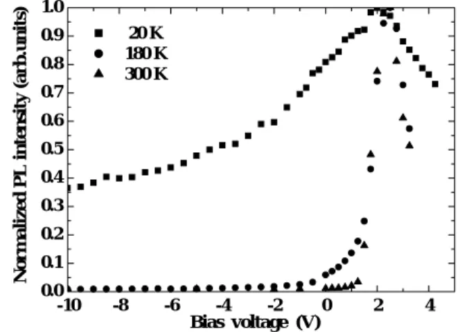
In order to directly examine the radiative recombination efficiency in the InGaN SQW layer, PL spectra were measured as a function of bias voltage at various temperatures under the direct excitation where only the SQW layer is selectively excited. At 20 K, for example, two emission bands at 540 nm (2.30 eV) and 525 nm (2.36 eV) are observed at 0 V in the PL spectra [12]. We note that the former peak coincident with the EL peak energy does not show any significant shifts with bias, probably due to the localized nature of the radiative recombination centers. On the other hand, the higher energy PL peak shows a Stark blueshift with increasing the reverse bias voltage, indicating the radiative recombination associated with the SQW confinement states. That is, the latter peak is located at 505 nm (2.46 eV) at -10 V, resulting in the reduced luminescence efficiency due to the tunnelling escape of carriers in spite of the fact that the QW potential is flattened as a result of the compensation of the piezoelectric field by the reverse field, as confirmed by Stark shifts. With increasing the forward bias, however, the PL efficiency increases and reaches the maximum around +2.5 V, as shown in Fig. 4. More importantly, with further increasing the forward bias the PL efficiency is significantly reduced as a result of carrier escape. This reduction is even enhanced at 180 and 300 K due to the phonon-assisted tunneling escape of carriers [14].
These results indicate that the EL efficiency is significantly influenced by interplay of the internal and external field effects on the carrier capture and escape processes in addition to the localization phenom- ena caused by In fluctuations in the SQW layer.
.
-10 -8 -6 -4 -2 0 2 4
0.0 0.1 0.2 0.3 0.4 0.5 0.6 0.7 0.8 0.9 1.0
Normalized PL intensity (arb.units)
Bias voltage (V) 20 K
180 K 300 K
These results of the EL as well as the PL efficiency variations with bias indicate that the carrier verti- cal escape from the localized recombination centres in the InGaN SQW-LED is crucial for the anoma- lously reduced EL efficiency, as schematically illustrated in Fig. 5, when the higher forward bias is nec- essary at lower temperatures. This is probably due to the hole trapping by deep acceptors at low tempera- tures and the resultant decreased hole conductivity in the diode.
Fig. 4 Integrated PL intensity normalized by the maximum value is plotted as a function of forward and reverse bias voltage at 20, 180, and 300 K. Note the existence of asymmetric external field effect, which is enhanced at higher temperatures.
4 Author, author, and author: Short Title
© 2005 WILEY-VCH Verlag GmbH & Co. KGaA, Weinheim
1 2 3 4 5 6 7 8 9 10 11 12 13 14 15 16 17 18 19 20 21 22 23 24 25 26 27 28 29 30 31 32 33 34 35 36 37 38 39 40 41 42 43 44 45 46 47 48 49 50 51 52
000000 physica (c) 0002/1 WordXP Art.: W0000/Autor\\Kitss001\Library\05_情報管理係\清水\著者最終原稿収集(海外出版社)\工
Forward bias:
increase of QW field
increase of tunneling
Reverse bias:
decrease of QW field increase of tunneling p n
QW
Zero bias:
existence of QW field
InGaN SQW within p-njunction LED
Forward bias:
increase of QW field
increase of tunneling
Reverse bias:
decrease of QW field increase of tunneling p n
QW
Zero bias:
existence of QW field
InGaN SQW within p-njunction LED
Forward bias:
increase of QW field
increase of tunneling
Reverse bias:
decrease of QW field increase of tunneling p n
QW
Zero bias:
existence of QW field
InGaN SQW within p-njunction LED p n
QW
Zero bias:
existence of QW field
InGaN SQW within p-njunction LED
4 Conclusion
The EL and PL efficiency of the InGaN SQW-LED has been investigated as a function of temperature and current (applied bias). Temperature dependence of the EL efficiency shows that under low and high injection currents its variation pattern with temperature drastically changes. That is, when the current is low and thus the forward driving voltage is very small, the EL quenching below 100 K is less significant or even absent due to the efficient carrier capture. However, for high injection current levels and thus large forward bias voltages, the EL quenching below 100 K persists. This unique dependence on tem- perature of the EL intensity variation at different injection levels originates from the difference in the forward bias voltage (external field effect). The changes of the PL efficiency with bias support this inter- pretation. These results imply that the unusual evolution of the EL intensity with temperature and current can be due to variations of the actual potential field distribution (due to both internal and external fields), which significantly influence the carrier capture efficiency within the SQW layer.
Acknowledgements The authors would like to thank Nichia Chemical Industry Ltd., especially S. Nakamura (presently at the University of California at Santa Barbara) for providing the chip samples used for the present study.
This work was supported in part by the Grant-in-Aid for Scientific Research from the Ministry of Education, Culture, Sports, Science and Technology (No.16360157).
References
[1] S. Nakamura and G. Fasol, The Blue Laser Diode, (Springer-Verlag Berlin Heidelberg, 1997).
[2] S. Nakamura, M. Senoh, N. Iwasa, S. Nagahama, T. Yamada, and T. Mukai, Jpn. J. Appl. Phys.(Part 2) 34, L1332 (1995).
[3] S. Chichibu, T. Azuhata, T. Sota, and S. Nakamura, Appl. Phys. Lett. 69, 4188 (1996).
[4] Y. Narukawa, Y. Kawakami, S. Fujita, S. Fujita, and S. Nakamura, Phys. Rev. B55, R1938 (1997).
[5] T. Mukai, K. Takekawa, and S. Nakamura, Jpn. J. Appl. Phys., Part 2 37, L839 (1998).
[6] K.P. O’Donnel, R.W. Martin, and P.G. Middleton, Phys. Rev. Lett. 82 , 237 (1999).
[7] T. Mukai, M. Yamada, and S. Nakamura, Jpn. J. Appl. Phys. 38 , 3976 (1999).
[8] A. Hori, D. Yasunaga, A. Satake, and K. Fujiwara, Appl. Phys. Lett. 79, 3723 (2001); J. Appl. Phys. 93, 3152 (2003).
[9] A. Hori, D. Yasunaga, A. Satake, and K. Fujiwara, Phys. Status Solidi A 192, 44 (2002)
[10] X.A. Cao, S.F. LeBoeuf, L.B. Rowland, C.H. Yan, and H. Lin, Appl. Phys. Lett. 82, 3614 (2003).
[11] P. Bakmiwewa, A. Hori, A. Satake, and K. Fujiwara, Physica E21, 636 (2004).
[12] A. Satake, A. Hori, Y. Takahashi, D. Yasunaga, and K. Fujiwara, in: A. R. Long, J. H. Davies (Eds.), Physics of Semiconductors 2002; Proceedings of the 26th International Conference on the Physics of Semiconductors, Ed- inburgh, 29 July-2 August 2002, Insitute of Physics Conference Series 171 (2002) D110.
[13] J. S. Im, H. Kollmer, J. Off, A. Sohmer, F. Scholz, and A. Hangleiter, Phys. Rev. B57, R9435 (1998).
[14] S. Machida, M. Matsuo, K. Fujiwara, J. R. Folkenberg, and J. M. Hvam, Phys. Rev. B67, 205322 (2003).
Fig. 5 Potential diagram of the InGaN SQW diode influ- enced by the piezoelectric field (left), while those under the forward and reverse bias conditions (right). Note that even under the forward bias condition the carriers can escape out of the well region due to the existence of piezo- electric field.