Akihiro TANABE†a), Masahiro HANMURA†, Takeyoshi KATOH†, Hironori OOMORI†, Akira HONMA†, andTeruhiko SUZUKI†,Nonmembers
SUMMARY A solution-processed photosensitive passivation layer with a low dielectric constant (PPLD) has been developed for an a-Si thin film transistor. The PPLD has three highly important properties: a low leakage current, low water absorption, and high-transparency. In addition to providing passivation, the PPLD doubles as a planarization layer. The photoactive property of the PPLD is convenient for its adaption to LCD manufacturing process. A photoactive compound contained in the PPLD enables the formation of contact holes and patterns via a photolithography process. Meanwhile, the PPLD requires ITO workability and strong adhe- sion property on metal and glass substrates. Apart from the above features, an a-Si TFT must perform with extremely high reliability if it is to replace the conventional inorganic passivation layer (SiNx:H). This reliability has been achieved by an a-Si TFT and LCD panel coated with the PPLD. A re- liability test was conducted under a high-temperature, high-humidity (HH) condition to examine how resistant the electronic characteristics were to change. The PPLD-coated LCD panel display view showed no defects for a test duration of HH200 hours. This high reliability was presumed to be at least partly attributable to the low water absorption rate of the passivation layer and the suppression of the increase of the TFT off-leakage current by the PPLD, a passivation layer designed to be non-polar as possible. Judging from the results of these experiments, this solution-processed passivation layer seems to be a viable substitute for the conventional inorganic passiva- tion layer. For a larger screen LCD and higher drive frequency, the problem of RC delay has been emerged. The low dielectric constant of the PPLD will suppress the RC delay of the signal and realize both a higher pixel and a higher drive frequency.
key words: passivation, a-Si, solution-processed, reliability
1. Introduction
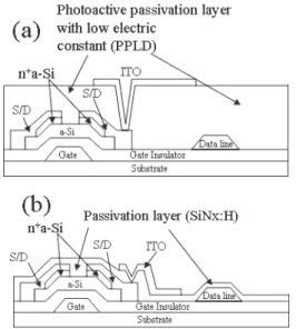
The growing need for friendlier environmental performance presses LCD panel manufacturers to improve their low- power-consumption technologies. Concurrently, LCD pan- els of larger sizes, higher pixel counts (e.g., 2K4K), and higher drive frequencies are emerging to meet the strong demand for high resolution and high quality. These new displays, however, are susceptible to degradation by RC de- lay. The PPLD has been developed as a coating passivation layer (Fig. 1). The low water absorption of the PPLD al- lows it to protect the a-Si layer and accordingly replace the conventional SiNx:H (Fig. 1). Further, the PPLD possesses has a low dielectric constant, a property that helps suppress the RC delay problem. The PPLD reduces reflection loss compared with the SiNx:H. by eliminating one layer. The stacking of layers with different refractive indexes confers
Manuscript received February 27, 2012.
Manuscript revised June 7, 2012.
†The authors are with Zeon Corporation, Kawasaki-shi, 210- 9507 Japan.
a) E-mail: [email protected] DOI: 10.1587/transele.E95.C.1737
Fig. 1 TFT structures passivated by the PPLD (a) and SiNx:H (b).
light reflectivity at the interface, which reduces the reflection loss. Meanwhile, the aperture rate can be increased and the relative intensity can be improved because the PPLD sup- presses the coupling effect between the data line and pixel electrode, enabling the ITO electrode area to expand relative to the conventional structure. Because the PPLD is coated by a solution process, the CVD process can be skipped. This suppresses the global warming effect, as the process requires no CVD cleaning gases (PFC, NF3), agents destructive to the ozone layer.
Figure 2 shows the process flows of the PPLD and SiNx:H. The PPLD requires fewer processes because it has a photosensitive function of the posi-type. The high trans- parency of the PPLD is maintained by bleaching, that is, by the degradation of photoactive compounds by exposure to light (g and i-lines). A baking time of 1 hour is recom- mended to cure the film.
2. Concept of the Material
One of the functions required of the passivation layer is to protect the a-Si layer from water and moisture. This is nec- essary mainly as a means of keeping the off-leakage current of the TFT low under a high-temperature, high-humidity condition. The layer deposited by the CVD process tends to be dense and compact, which allows it to protect the a- Copyright c2012 The Institute of Electronics, Information and Communication Engineers
Fig. 2 Process flows of the PPLD and SiNx:H.
Fig. 3 Material structures of an acrylic polymer and the PPLD.
Si layer from water intrusion. A solution-processed layer is less effective in protecting the a-Si layer from intruding wa- ter, as it tends to have a low density. Given the difficulty in fabricating solution-processed layers with densities similar to inorganic layers, we decided to design a new molecular structure. Specifically we wanted a hydrophobic structure to reduce the level of water absorption. Another group has reported the development of a non-photoactive type of pas- sivation layer [2]. We believe, however, that a photoactive type of passivation is more suitable for patterning the con- tact holes to wire up the pixel electrodes. Yet photoactive compounds have a polar property which tends to come hand in hand with a high water absorption. Our solution was to develop a non-polar base polymer using an olefin type of polymer (see Fig. 3). For comparison, we also prepare a conventional acrylic polymer to investigate the correlation among hydrophilicity, water absorption, and the off-leakage current of the TFTs of the passivation layer.
3. Experiments
3.1 Film Properties
3.1.1 Electric Characteristics
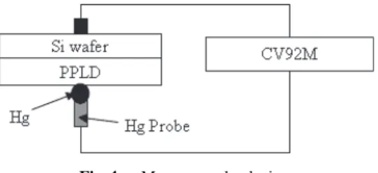
The PPLD and acrylic polymers were coated on Si sub- strates (low resistivity Si wafer), and soft-baked at 100◦C and 90◦C, respectively, bleached over 1 J/cm2, and finally cured at 230◦C in an N2 oven. The electric characteristics
Fig. 4 Mercury probe device.
(breakdown voltage and dielectric constant) were measured respectively by a mercury probe device which has high re- peatability (see Fig. 4). This device doesn’t requires to fab- ricate a electrode, thus it doesn’t damage the surface of the PPLD. The PPLD was formed on a low resistivity Si wafer.
The Hg probe was positioned in contact with the PPLD.
3.1.2 Water Absorption
The coefficient of water absorption of the PPLD and acrylic polymer passivation layers was measured by thermal des- orption spectroscopy (TDS). Each material was exposed to a high-temperature, high-humidity (HH) condition, (60◦C, 90%RH) for 48 hours. TDS measurement was conducted before and after the exposure to the HH condition.
3.1.3 Transmittance
The PPLD and acrylic polymer were coated on glass. Af- ter curing, the transmittance was measured by UV-vis spec- troscopy from 300 nm to 700 nm.
3.2 Amenability to LCD Array Processing 3.2.1 Photolithography Characteristics
A PPLD coated on glass (Corning Eagle XG) was soft- baked at 100◦C for 2 minutes and exposed to a mixed light of the g, h, and i lines. The holes were then developed with an 0.4% TMAH solution at 23◦C for 90 seconds. The hole patterns were observed by a Scanning Electron Microscope (SEM). Holes of 5µm in diameter were arranged on a pho- tomask, and the PPLD film was bleached over 1 J/cm2 for the g, h, and i lines. The retention rate of the contact holes was measured after curing the layer at 230◦C for 1 hour in an oven (N2 atmosphere). The final thickness was about 2.1µm.
3.2.2 ITO Pattern Workability
An ITO film was deposited by the sputtering method on a PPLD-coated sheet of glass. Next, the ITO was patterned by a photolithography process and subsequent etching pro- cess with 20% aqua regia at 40◦C. After stripping the photo resist with a general stripper ST106 at 60◦C, the substrate was annealed at 220◦C in a nitrogen atmosphere. The ITO patterns were observed by an optical microscope.
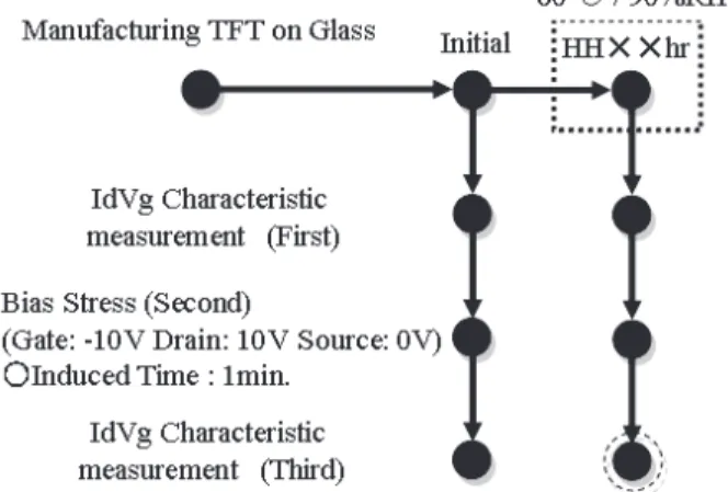
Fig. 5 Method for evaluating the TFT characteristics.
3.3 TFT Characteristics
A back channel etched inverted-staggered type TFT was fabricated. The gate, source, and drain were deposited by sputtering and then patterned by a standard photolithogra- phy process. Three layers, i.e., a layer of SiNx:H, a layer of a-Si:H, and a layer of n+a-Si:H were deposited one by one in a cat-CVD reactor. The n+-a-Si of the back channel was etched by wet etching with HF/HNO3/H2O. The gate con- tact hole was patterned by a standard photolithography and a dry etching process with an etching gas of SF6 (to etch the gate insulator). Once these processes were finished, the PPLD was coated over the TFT devices. Because the PPLD is photoactive, hole patterns can be fabricated photolitho- graphically. After spin coating and soft-baking at 100◦C, the PPLD was exposured to the mixed light of the g, h, and i lines. Then the holes were developed in 0.4% TMAH for 90 seconds. The hole patterns were observed by SEM. Next, TFT devices passivated with PPLD were exposed to an HH condition (60◦C, 90%RH) for a certain period of time.
The TFTId-Vgcurrent measurement was measured by a semiconductor parameter analyzer B1500A (Agilent Tech- nologies). The channel size was L/W=5µm/14µm (actual measurement). The measurement took place in a cycle of three steps (see below). First, an initialId-Vgmeasurement was carried out: Vg = −10 V∼+15 V,Vd = 10 V. Second, a voltage stress ofVg =−10 V,Vd= 10 V,V s =0 V was applied for 1 minute to simulate a TFT off-state, in order to more closely evaluate the panel driving condition. It is im- portant to investigate the stress when the TFT is an off-state, given that the TFT degradation is closely correlated with the TFT off- leakage current, as discussed below. Third, theId- Vgmeasurement was carried out (under the same measure- ment conditions used for first step). This cycle was repeated for a certain period under the HH condition. The off-leakage current was defined as the minimum current.
Figure 5 shows the method used to evaluate the TFT measurement.
3.4 LCD Panel Evaluation
An LCD test panel was fabricated to examine the validity of the LCD array fabrication process and the reliability of the PPLD. The resolution was 80(H)×80(V) and the pixel size was 0.4 mm(H)×0.4 mm(V). The color mode was black- and-white and the mode of the LC was twisted nematic.
3.5 RC Delay Calculation
The RC delay of the data line signals of the LCD with each passivation layer was calculated. Figure 6 shows the equiva- lent circuit. The signal voltage at the far end of the data line was obtained from Eq. (1)
V(t)=10{1−exp(−t/RC)} (1)
Where,V(t) is the signal voltage,Ris a sum of the resistance of the data wire,Cis a sum of the parasitic capacitance (sim- ulates between data lines and ITO electrodes),tis time, and the input signal is 10 V.
4. Results and Discussions
4.1 Film Properties
4.1.1 Electric Characteristics
The passivation layer needs a low off-leakage current prop- erty at 2.0 MV/cm. The PPLD and acrylic polymer both show a lower off-leakage current than the SiNx:H, the passi- vation layer conventionally used for the a-Si TFT. The PPLD meets the requirement (Fig. 7).
The PPLD shows a low dielectric constant compared to the acrylic polymer and SiNx:H (Fig. 8).
This result is derived from the material structure of the PPLD. As mentioned earlier, the PPLD was designed to be more nonpolar than the acrylic polymer. This low polarity reduces the dielectric constant of the PPLD.
4.1.2 Water Absorption
Figure 9 shows the amount of water absorption of each pas- sivation layer. Compared with acrylic polymer, the PPLD exhibited a lower coefficient of water absorption. This could be explained by the higher polarity of the acrylic polymer, a property linked to its polar ester bonds.
4.1.3 Transmittance
Figure 10 shows the transmittance of each passivation layer.
Fig. 7 Off-leakage current versus electric field of MOS capacitors coated with SiNx:H, acrylic polymer and the PPLD.
Fig. 8 Dielectric constant of PPLD and acrylic polymer.
Fig. 9 Water absorption rate measured by TDS (PPLD and acrylic polymer).
The PPLD showed higher transparency than the acrylic polymer at the 400 nm wavelength. This was attributed to the olefin-type polymer framework of the PPLD, a feature selected to confer a non-resonant, noncrystalline structure.
4.2 Amenability to LCD Array Processing 4.2.1 Photolithography Characteristics
Table 1 shows photolithographic characteristics of the PPLD. A high photo speed is always required to manufac- ture LCD panels. By controlling the polymer acidity and materials, the photo speed can be changed. The hole pat- terns were formed by a photolithographically, and were well maintained after curing (Fig. 11). This means that the PPLD
Fig. 10 Transmittance of the PPLD and acrylic polymer.
Table 1 Photolithographic characteristics of the PPLD.
Fig. 11 Shape of the PPLD contact hole after development and after curing.
can provide drain-contact holes for an LCD array substrate.
4.2.2 ITO Pattern Workability
The high adhesion between the passivation layer and sub- strate prevents the former from peeling during the fabrica- tion of the TFT array. The passivation layer also requires adequate resistance to both the etchant for ITO and the re- sist remover. Inadequate resistance to either would prevent the high-accuracy patterning of the ITO electrode. Thus, the PPLD is required for ITO pattern workability.
Figure 12 shows a patterned ITO on a PPLD. The shapes of the patterns are accurate and free of defects. This result proves that an ITO can be patterned on a PPLD.
4.3 TFT Characteristics
Figure 13 shows the time-dependent off-leakage current characteristics of a TFT with acrylic polymer, SiNx:H, and PPLD. The off-leakage current was defined as the value of the smallest Id current of the third measurement. All of the devices showed goodId-Vgcharacteristics before exposure
Fig. 12 (a) Cross-section view of ITO patterning process (graphic) and (b) top view of a patterned ITO on a PPLD (photograph).
Fig. 13 Time-dependent off-leakage current characteristics (after 1minute bias) of TFTs with acrylic Polymer, SiNx:H, and PPLD under a high- temperature, high humidity condition (60◦C, 90%RH). Measurement con- dition:Vg=−10 V∼+15 VVd=10 V.
to high-temperature, high- humidity (60◦C, 90%RH). The off-leakage current of the TFT with the acrylic polymer be- gan to increase after 20 hours under the HH condition and rose progressively to 1E-11A by around 50 hours. In con- trast, the off-leakage currents of the SiNx:H and the PPLD remained low after over 1,000 hours under the HH condi- tion. One of the factors presumed to be responsible for this suppression of off-leakage current was the low water absorp- tion rate of the passivation layer, as described before [3]. In fact, the PPLD absorbs less water than the acrylic polymer.
The SiNx:H layer deposited by the CVD process tends to be dense and compact, which protects the a-Si semiconduc- tor layer from the intrusion of external water. The PPLD, in turn, is composed of a less hydrophilic group than the acrylic polymer, and thus retains a low level of water ab- sorption.
4.4 LCD Panel Evaluation
Table 2 shows the specifications of the LCD test panel.
4.4.1 TFT Characteristics of the Test Patterns
Figure 14 shows initial data on the TFTId-Vgcharacteris- tics of the test patterns for the PPLD and SiNx:H-passivated
Fig. 14 TFT Id-Vg characteristics of test patterns of the PPLD and SiNx:H-passivated TFT.Vd=10 V.
TFT. The TFT array processes were the same but the passi- vation processes differed (the PPLD was formed by a coat- ing process and the SiNx:H was formed by a CVD process).
The TFT channel size was L/W=3/14µm (actual measure- ment). As the PPLD was coated via a solution-process, it suppressed damage to the a-Si more effective than the SiNx:H fabricated by the CVD plasma process. Thus, the Vth, S-value, and On/Offratio of the PPLD were superior to those of the SiNx:H-passivated TFT, along with several other properties.
4.4.2 Appearance of the LCD Panel Display
No remarkable problems were observed in the initial display operations of the LCD panel manufactured with the PPLD.
Figure 15 shows a black-mode of the first LCD panel fabri- cated with a PPLD as a passivation layer. The appearance of the panel display was unchanged after exposed to the high- temperature, high-humidity condition (60◦C, 90%RH) for about 200 hours. This demonstrated that the reliability of the LCD panel was closely correlated with the reliability of the TFT. It also confirmed that the PPLD could protect the a-Si layer from water.
Fig. 15 LCD panel in black mode fabricated with a PPLD: (a) initial, (b) After 200 hours (60◦C, 90%RH) driving condition: Vg(on)=12.5 V, Vg(off)=−12.5 VVcom=−0.8 V, frame-reverse driving.
Fig. 16 Calculated rise times of the data lines at the far end.
4.5 RC Delay Calculation
RC signal delay has emerged as a problem for larger-screen LCDs and LCDs with higher drive frequencies. RC de- lay on the gate line is thought to be more critical than that of the data line. Here, however, we focused on the de- lay of the data line, as this takes up larger areas where the PPLD was formed (see Fig. 1). The RC delay of the data line is caused by the capacitance of the data lines, a property which depends on the dielectric constant of the or- ganic layer. Thus, a lower-dielectric-constant material is preferred. The RC delay of the data line signals of LCD was calculated for three types, namely, (1) the PPLD, (2) the acrylic polymer/SiNx:H, (3) the SiNx:H, as shown in Fig. 16.
The parasitic capacitance of the data line is presumed to be the capacitance between the data lines and common elec- trodes. Figure 15 shows the calculation results of the rise time of the data lines at the far end. These results indicate that the data line on the LCD coated with the PPLD has less of an RC delay than that on the LCD coated with the acrylic polymer of SiNx:H. We thus see that the new structure with the PPLD improved the moving image characteristics of a large-size LCD.
Acknowledgments
The authors would like to express their gratitude to Prof.
Matsumura and Dr. Ohdaira of JAIST (Japan Advanced In- stitute of Science and Technology) for their kind support of our project.
[1] K. Sugitani, et al., “Photo-sensitive passivation layer for a-Si TFT of LCD with characteristics of low dielectric constant,” IDW’08, P1853, 2008.
[2] A. Krishnamoorthy, et al., “Solution processable passivation layer for active matrix thin film transistor on rigid and flexible substrates,”
SID’08, P140, 2008.
[3] K. Sugitani, et al., “Reliability improvement of a-Si TFT using low water absorption type of photosensitive passivation layer with low di- electric constant,” IDW’09, FMCp-23, 2009.
Akihiro Tanabe received B.S. and M.S. de- grees in Science and Engineering from Waseda University in 2004 and 2006, respectively. He now works at Zeon Corporation.
Masahiro Hanmura received B.S. and M.S.
degrees in Biotechnology from the Tokyo Insti- tute of Technology in 1994 and 1996, respec- tively. He was employed by Dai Nippon Print- ing Co., Ltd. From 1996 to 1999 and Seiko Ep- son Corporation from 1999 to 2005. He now works at Zeon Corporation.
Takeyoshi Katoh received B.S. and M.S.
degrees in Engineering from Tokai University in 1991 and 1993, respectively. From 2001–
2004, he researched semiconductor manufactur- ing technology at the Ohmi Lab. of Tohoku Uni- versity. He now works at Zeon Corporation, Inc.
Hironori Oomori received B.S. and M.S.
degrees in Polymer Science Engineering from the Tokyo Institute of Technology in 1994 and 1996, respectively. From 1996 to 2002, he worked as a researcher for TOPPAN PRINTING Co., Ltd. He now works at Zeon Corporation.
Teruhiko Suzuki received B.S. and M.S.
degrees from the School of Engineering at To- hoku University in 1988 and 1990, respectively.
He now works at Zeon Corporation