Statistical Analysis of RTS Noise and Low
Frequency Noise in 1M MOSFETs Using an
Advanced TEG
著者
Abe K., Sugawa S., Watabe S., Miyamoto N.,
Teramoto A., Toita M., Kamata Y., Shibusawa
K., Ohmi T.
journal or
publication title
AIP Conference Proceedings 19th International
Conference on NOISE AND FLUCTUATIONS-ICNF2007
volume
922
page range
115-118
year
2007
URL
http://hdl.handle.net/10097/51830
Statistical Analysis of RTS Noise and
Low Frequency Noise in 1M MOSFETs
Using an Advanced TEG
K. Abe
1, S. Sugawa
1, S. Watabe
1, N. Miyamoto
2, A. Teramoto
2,
M. Toita
3, Y. Kamata
4, K. Shibusawa
4and T. Ohmi
21Graduate School of Engineering, Tohoku University
2New Industry Creation Hatchery Center, Tohoku University, Aza-Aoba 6-6-10, Aramaki, Aoba-ku,
Sendai, 980-8579, Japan, [email protected]
3Asahi Kasei Electronics Co., Ltd., 5-4960, Nakagawara-cho, Nobeoka, Miyazaki, 882-0031, Japan 4Miyagi Oki Electric. Co., Ltd., 1, Okinodaira, Ohira-mura, Kurokawa-gun, Miyagi, 981-3963, Japan
Abstract. In this paper, we developed an advanced Test Element Group (TEG) which can
measure Random Telegraph Signal (RTS) noise in over 106 nMOSFETs including various gate
sizes with high accuracy in a very short time. We measured and analyzed these noises statistically, as the result, we confirmed that appearance probabilities in the TEG and noise intensities of RTS are dependent on gate sizes.
Keywords: MOSFET, RTS noise, Test Element Group, Statistical Analysis PACS: 73.50.Td, 72.20.Jv
INTRODUCTION
Random Telegraph Signal (RTS) noise and low frequency noise caused by RTS have become serious issues in electronic circuit design with downscaling of CMOS device [1-3]. They induce a degradation of signal-to-noise ratio in overall analog circuits, such as an increase of phase noise in oscillators for wireless applications. Recent years, it has been reported that an image quality degradation in a CMOS image sensor from random noise caused by RTS, which is difficult to eliminate by established noise reduction circuitry [2]. Then statistical analysis of RTS noise is indispensable for theoretical elucidation of the physical origin of RTS and its noise reduction. However, we can not find the MOSFET showing RTS behavior frequently and the statistical analysis of the noise characteristics has been difficult actually until today because the measurement system becomes so complex and it needs very long time to measure a sufficient number of samples which are element device forms.
In this work, we developed a new Test Element Group (TEG) which can measure both variation of stationary electrical characteristics [4] and noise characteristics in a large number of MOSFETs. Using this TEG, we have measured and analyzed statistically noise characteristics of the total of 106 MOSFETs. We first measure
entire noise characteristics of the MOSFETs in a short time (about 4 minutes), and
115
Downloaded 07 Aug 2011 to 130.34.134.250. Redistribution subject to AIP license or copyright; see http://proceedings.aip.org/about/rights_permissions
CREDIT LINE (BELOW) TO BE INSERTED ON THE FIRST PAGE OF EACH PAPER EXCEPT THE PAPER ON PP. 473 - 478
CP922, Noise and Fluctuations, 19th International Conference, edited by M. Tacano, Y. Yamamoto, and M. Nakao
© 2007 American Institute of Physics 978-0-7354-0432-8/07/$23.00
CREDIT LINE (BELOW) TO BE INSERTED ONLY ON THE FIRST PAGE OF THE PAPER ON PP. 473 - 478
then we can find easily and analyze a specific MOSFET having anomalous noise behavior individually. In the result, we discuss the dependences of appearance probabilities of RTS and amplitudes of RTS in the TEG on the gate size.
TEG STRUCTURE AND MEASUREMENT METHOD
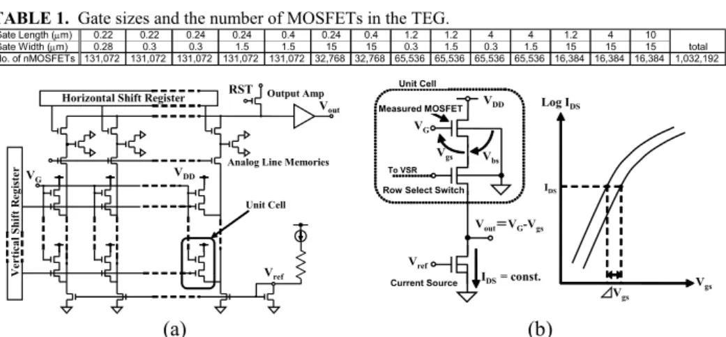
The circuit schematic of the TEG is shown in Fig. 1 (a). Values of applied bias voltage to the measured MOSFETs (VG, VDD) are fixed and the voltages are forced
simultaneously. The operating points of the MOSFETs are controlled by IDS given by
the current sources which are placed at every column. Electrical characteristics of the MOSFETs can be observed as the Vgs included in the output voltage Vout (Fig. 1 (b)).
When a particular cell has a RTS behavior, we can specify and observe them as Vgs
fluctuation in time-scale by the result of continuous sampling with adequately small sampling rate. The key point for fast read-out is that the output signal from a cell is not the “current” but the “voltage” signal and they are converted to digital data by Analog / Digital converter near the TEG. Therefore, we can easily measure noise characteristics of 106 MOSFETs in a short time (0.7 s per 1 scan) by use of the
horizontal and the vertical shift registers. We can also sample the value of Vgs of a
specified MOSFET every 0.33 µs continuously.
We designed the TEG that includes 15 gate sizes of nMOSFETs as shown in Table 1 and manufactured the TEG by 0.18µm, 1 Poly 2 Metal standard CMOS technology.
TABLE 1. Gate sizes and the number of MOSFETs in the TEG.
FIGURE 1. (a) Circuit schematic of the proposed TEG and (b) Measurement method of Vgs fluctuation
of a MOSFET in the TEG.
RESULTS AND DISCUSSION
To examine the random noise from RTS distribution of the TEG, we use the standard deviations of the continuous 300-time outputs from each MOSFET (σR) as
the random noise indicator. The distribution of σR in Fig. 2 shows a NOT gaussian
distribution and a specific tail in high σR region. Figure 2 also shows time-domain
plots of Vgs for particular cells on the random noise distribution. Vgs behaviors for the
Gate Length (µm) 0.22 0.22 0.24 0.24 0.4 0.24 0.4 1.2 1.2 4 4 1.2 4 10
Gate Width (µm) 0.28 0.3 0.3 1.5 1.5 15 15 0.3 1.5 0.3 1.5 15 15 15
No. of nMOSFETs 131,072 131,072 131,072 131,072 131,072 32,768 32,768 65,536 65,536 65,536 65,536 16,384 16,384 16,384 1,032,192total
Vref
Vout
RST
VG VDD
Horizontal Shift Register
V erti cal Sh if t R eg ist er Output Amp
Analog Line Memories
Unit Cell Vout=VG-Vgs VG Vref VDD Current Source Row Select Switch
Vgs IDS = const. To VSR Log IDS Vgs IDS ⊿Vgs Measured MOSFET Unit Cell Vbs (a) (b) 116
cells having large σR become two-level quantum change randomly. These phenomena
indicate the RTS noise, which is caused by capturing and emitting a carrier on a trap near the Si/SiO2 interface. We measured various MOSFETs which show RTS
behaviors in the TEG and extracted their RTS parameters including amplitudes (∆Vgs),
mean time to capture (<τc>) and to emission (<τe>). Then, signal transition
probability is defined by the following equation [5]
(
< >+< >)
⋅ > >< < = 2 c e c e T τ τ τ τ (1)Here, ∆Vgs*T is considered as a factor to characterize RTS noise intensity of a
MOSFET. Figure 3 shows correlation diagram between σR and ∆Vgs*T. There is
strong correlation clearly. Therefore the origin of increasing σR is regarded as RTS
noise and σR is available to find cells having RTS noise easily. And then, values of
∆Vgs*T vary widely under same gate area and same bias condition. It indicates that
the energy level of traps and the distance from Si/SiO2 interface are distributed.
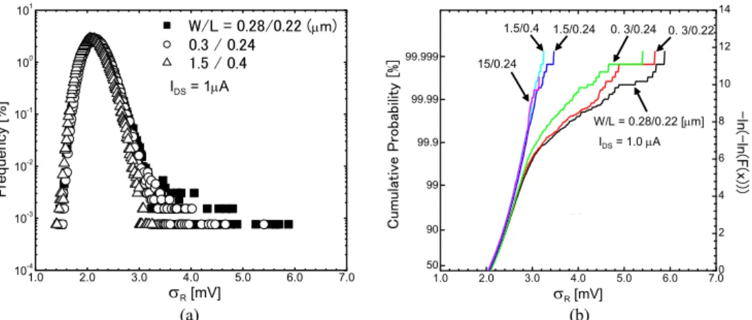
The distributions of σR for several gate sizes are shown in Fig. 4 (a). The tails
FIGURE 2. Distribution of the standard deviation of Vgs fluctuation for one MOSFET in time-scale
(σR) with W/L=0.3/0.22 [µm] and time-domain Vgs behaviors for particular cells.
FIGURE 3. Correlation diagram between σR and ∆Vgs*T when sampling rate = 3 MHz (sampling cycle
= 0.33 µs). 0 1 2 3 4 5 6 7 1x10⁻⁴ 1x10⁻³ 1x10⁻² 1x10⁻¹ 1x100 1x101 σR[mV] Freque n cy [% ] W/L = 0.3/0.22 [µm] IDS= 1µA 0.65 0.70 0.75 Time [ms] Vgs [V ] 0 0.2 0.4 0.6 0.8 1.0 0.60 0.65 0.70 0 0.2 0.4 0.6 0.8 1.0 Time [ms] Vgs [V] 0.55 0.60 0.65 0 0.2 0.4 0.6 0.8 1.0 Time [ms] Vgs [V ] 0.65 0.70 0.75 0 0.2 0.4 0.6 0.8 1.0 Time [ms] Vgs [V] 0.00 2.00 4.00 6.00 0.0 0.5 1.0 1.5 2.0 2.5 3.0 ∆
V
gs *T
[mV]
σR[mV]
W/L=0.28/0.22 [µm] IDS =1.27 [µA]appear prominently as gate area becomes smaller. This tendency becomes clear by representing same distributions as Gumbel distributions, which is used in the extreme statistics (Fig. 4 (b)) [3]. The distributions for small gate MOSFETs are fit into straight lines in the range of σR > 3 mV. This means that the appearance probability
of MOSFETs having critical RTS noise for circuit operations could be described by the theory of Gumbel distribution statistically and we may be able to predict and control RTS noise in ULSI to avoid the harmful effect of the noise.
CONCLUSION
In this work, we developed an advanced TEG for statistical analysis of RTS and we can easily find the cells having large RTS noise in over 106 nMOSFETs from the distribution of σR, which is supposed an indicator to show RTS noise intensity briefly
and shortly. From the result, we found that appearance probabilities of RTS become larger as shrinking of the gate size. The quantitative information given by the TEG is very useful for understanding the physical origin of RTS and circuit-level RTS noise behaviors in the process and the device development or electronic circuit design
REFERENCES
1. M. J. Kirton and M. J. Uren, “Noise in Solid-State Microstructures: A New Perspective on Individual Defects, Interface States, and Low-Frequency Noise,” Adv. in Phys., 38, 367-468, 1989. 2. X. Wang, P. R. Rao, A. Mierp, Albert J. P. Theuwissen, “Random Telegraph Signal in CMOS
Image Sensor Pixels,” Tech. Dig. of IEDM '06, IEEE, 2006, pp. 115-118.
3. N. Tega, H. Miki, T. Osabe, A. Kotabe, K. Otsuga, H. Kurata, S. Kamohara, K. Tokami, Y. Ikeda, R. Yamada, “Anomalously Large Threshold Voltage Fluctuation by Complex Random Telegraph Signal in Floating Gate Flash Memory,” Tech. Dig. of IEDM '06, IEEE, 2006, pp. 491-494. 4. S. Watabe, S. Sugawa, A. Teramoto, T. Ohmi, Jpn. J. Appl. Phys., 46, 4B, 2054-2057 (2007). 5. C. Leyris, F. Martinez, M. Valenza, A. Hoffmann, J.C. Vildeuil, F. Roy, “Impact of Random
Telegraph Signal in CMOS Image Sensors for Low-Light Levels,” Proceedings of the 32nd European Solid-State Circuits Conference ESSCIRC 2006, IEEE, 2006, pp. 376-379.
1.0 2.0 3.0 4.0 5.0 6.0 7.0 10-4 10-3 10-2 10-1 100 101 F requency [%] σR [mV] W/L = 0.28/0.22 (µm) 0.3 / 0.24 1.5 / 0.4 IDS = 1µA 1.0 2.0 3.0 4.0 5.0 6.0 7.00 2 4 6 8 10 12 14 IDS = 1µA C umul ati ve Pr o babi lity [ % ] -l n(-ln(F(x))) σR [mV] 50 90 99 99.999 99.9 99.99 0. 3/0.24 1.5/0.24 1.5/0.4 15/0.24 W/L = 0.28/0.22 [µm] 0. 3/0.22 IDS= 1.0 µA
FIGURE 4. (a) Distributions of σR and (b) Gumbel distributions of σR with several gate sizes.
(b) (a)
118
![FIGURE 2. Distribution of the standard deviation of V gs fluctuation for one MOSFET in time-scale (σ R ) with W/L=0.3/0.22 [µm] and time-domain V gs behaviors for particular cells](https://thumb-ap.123doks.com/thumbv2/123deta/5931936.1052303/4.755.112.649.80.299/figure-distribution-standard-deviation-fluctuation-mosfet-behaviors-particular.webp)