Properties of light-emitting porous silicon photoetched in aqueous
HF/ FeCl
3solution
Yan Kai Xu and Sadao Adachia兲
Department of Electronic Engineering, Faculty of Engineering, Gunma University, Kiryu-shi, Gunma 376-8515, Japan
共Received 23 January 2007; accepted 14 March 2007; published online 18 May 2007兲
The formation of yellow-light-emitting porous silicon共PSi兲 layers in a HF solution with adding an oxidizing agent FeCl3 is presented. The PSi layers are formed by photoetching under Xe lamp illumination. The photoluminescence 共PL兲 intensity is strongly dependent on the FeCl3 concentration and shows a maximum at x⬃25 wt % 关50 wt % HF:共x wt % FeCl3in H2O兲=1:1兴. The surface topography as characterized by atomic force microscopy reveals features on the order of 20⫺100 nm with a root-mean-squares roughness of ⱕ2 nm. The Fourier-transform infrared spectroscopy shows a new absorption peak at⬃1100 cm−1, which is assigned to the surface oxide stretching mode and grows larger with increasing etching time. The stain etched samples also show PL emission, but they are synthesized only at higher x concentrations 共ⱖ20 wt %兲. The PSi formation mechanism can be explained with the aid of a surface energy-band diagram of n-type silicon in the HF/ FeCl3 electrolyte. © 2007 American Institute of Physics.
关DOI:10.1063/1.2733752兴
I. INTRODUCTION
Visible light emission from porous silicon 共PSi兲 ob-served at room temperature has provoked a sustained search for its potential application in silicon-based optoelectronic devices and its academic interest.1,2 Such luminescent PSi layers are commonly formed by anodic etching on p-type silicon substrates. The first report of a luminescent porous layer obtained without electrochemical anodization came from Sarathy et al.3who used a stain etching in a HF/ HNO3 solution. Noguchi and Suemune4demonstrated the formation of a luminescent PSi spot by photoetching in a HF solution under He-Ne laser illumination for ⬃60 min. Subsequently, Yamamoto and Takai used a mixture of HF/ H2O2 to obtain efficient PSi in short He-Ne illumination time 共⬃10 − 30 min兲.5,6
More recently, Koker and Kolasinski7used the circular-pattern radius produced by a 15 mW He-Ne laser to measure the photoetching rate of n-type Si共111兲 in various fluoride solutions. They also investigated the etching mecha-nisms of n- and p-type Si共111兲 in aqueous HF solutions un-der a continuous wave or a pulse laser irradiation of wave-lengths 365, 473, 532, 633, 685, and 730 nm.8
In this article we report on a simple fabrication method of luminescent PSi layers on n-type silicon substrates. The PSi layer is formed by photoetching in a HF/ FeCl3solution under Xe lamp illumination. The use of a Xe lamp enables a formation of large, homogeneous PSi layers. The addition of oxidant FeCl3 in HF results in a stable formation of PSi layers in very short time. Properties of the photoetched PSi layers are characterized using photoluminescence 共PL兲, atomic force microscopy 共AFM兲, and Fourier-transform in-frared spectroscopy共FTIR兲.
II. EXPERIMENT
Figure 1 shows an experimental arrangement used for the PSi formation by photoetching in a HF/ FeCl3 solution. The silicon substrates used were n-type Si共100兲 with a resis-tivity range of 1 − 3⍀ cm. They were degreased using or-ganic solvents, followed by oxide removal with 50% HF solution, and then rinsed in de-ionized water.
Photoetching was performed at room temperature in an ultrasonic bath. The sample surface was illuminated by a 300 W Xe lamp through an optical filter blocking wavelengths shorter than 0.6m. The chemical etchant used was 50 wt % HF solution adding an oxidizing agent of FeCl3x in wt % in H2O 关50 wt % HF:共x wt % FeCl3in H2O兲=1:1 in volume ratio兴. After photoetching, the samples were rinsed in de-ionized water. The thickness of the PSi film was measured using a Talystep profilometer after a part of the film was removed by 2% NaOH solution.
PL measurements were performed using a grating spec-trometer and a Peltier-device-cooled photomultiplier tube
a兲Electronic mail: adachi@el.gunma-u.ac.jp
FIG. 1. 共Color online兲 Experimental apparatus used for PSi formation by photoetching in a HF/ FeCl3solution. Photoetching was performed under Xe
lamp illumination through an optical filter cutting lights ofⱕ0.6m.
共Hamamatsu R375兲. The 325 nm line of a He–Cd laser 共Kimmon IK3302R-E兲 chopped at 329 Hz was used as the excitation light source. The surface morphology of PSi sample was investigated by ex situ AFM, using a Digital Instruments Nanoscope III in the tapping mode and in the repulsive force regime. The surface chemistry of the PSi samples was monitored by FTIR. The FTIR spectra were recorded using a Nicolet Magna 560 spectrometer in the 400− 2000 cm−1 region with a resolution of 4 cm−1.
III. RESULTS AND DISCUSSION A. Photoluminescence
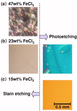
We first discuss the effect of the FeCl3concentration on the PL emission intensity. The FeCl3concentration was var-ied from x = 10 to 47 wt % in the 50 wt % HF solution. The samples were immersed in each solution for t = 1 min with and without Xe lamp illumination. The results of these ex-periments are summarized in TableI. The corresponding sur-face morphologies observed by optical microscopy are shown in Fig.2. It is well known that aqueous HF solution does not attack silicon harshly, but etches SiO2rapidly. The
addition of a sufficient quantity of an oxidizing agent may lead to the oxidation of the silicon surface, resulting in sili-con etching. More highly sili-concentrated FeCl3may thus lead to more vigorous etching of the silicon substrate.
We can see in Table I that the sample etched at x ⱕ15 wt % without Xe lamp illumination 共stain etching兲 does not show PL emission. On the other hand, the samples pho-toetched in the x = 10− 47 wt % solutions show PL emission and their intensity becomes maximum at x = 23 wt % solu-tion. We, however, found that large and homogeneous PSi layers can be more easily formed by photoetching in the x = 15 wt % solution than in the 23 wt % solution 关cf. Figs.
2共b兲 and2共c兲兴. Thus, the results presented in the following are mainly obtained by photoetching in the x = 15 wt % solu-tion. It should also be noted that the sample etched in the high FeCl3 共x=47 wt %兲 solution provides heavily stained surface morphology 关Fig.2共a兲兴.
The room-temperature PL spectra of PSi photoetched in HF/ FeCl3 solutions with x = 23 wt % and 47 wt % for t = 1 min, together with those obtained by stain etching in the same solutions for t = 1 min are shown in Fig.3. Note that the high energy tails seen in Figs. 3共b兲 and3共c兲come from the exciting light source共He–Cd laser兲. It is found that the pho-toetched PSi spectra 关Figs. 3共a兲 and 3共c兲兴 exhibit a broad
emission peaking at ⬃2.0−2.1 eV, which is typically ob-served in stain etched PSi samples in HF/ HNO3-based solutions.3,9–14The stain etched sample in the 47 wt % solu-tion关Fig.3共d兲兴 also exhibits a broad peak at ⬃2 eV. On the other hand, the very weak PL emission from the stain etched sample in the 47 wt % solution 关Fig. 3共b兲兴 shows a broad peak at ⬃1.8 eV, which is typically observed in anodic PSi samples in HF/alcohol-based solutions.1,2,15–18
Figure 4共a兲 plots the PL intensity versus photoetching time t for PSi formed in a HF/ FeCl3 solution with x = 15 wt %. It is seen that the PL intensity increases with increasing t and shows a saturation at t⬃2 min. Note that the PSi formation time t⬃2 min is much shorter than those formed in pure HF or a mixture of HF/ H2O2 共t ⬃10–30 min兲 using a coherent light source 共He–Ne laser兲.4–6
TABLE I. PL intensity for samples formed by stain and photoetching in solutions with adding an oxidizing agent of FeCl3 x in wt % in H2O
关50 wt % HF:共x wt % FeCl3in H2O兲=1:1 in volume ratio兴.
Etching
x wt % FeCl3in H2O
10 15 23 47
Stain No emission No emission Very weak Weak
Photoetching Weak Moderate Strong Weak
FIG. 2. 共Color online兲 Surface view of n-type silicon samples observed by an optical microscopy共⫻100兲. 共a兲 Stain etched in HF/FeCl3solution with x = 47 wt %共t=1 min兲, 共b兲 stain and photoetched in HF/FeCl3solution with
x = 23 wt % 共t=1 min兲, and 共c兲 photoetched in HF/FeCl3 solution with x
= 15 wt %共t=3 min兲.
FIG. 3. PL spectra of PSi photoetched in HF/ FeCl3 solutions with x
= 23 wt % and 47 wt % for t = 1 min, together with those obtained by stain etching in the same solutions for t = 1 min.
The PL peak energy versus immersion time t in a HF/ FeCl3 solution is shown in Fig.4共b兲. A gradual increase in the peak energy from⬃1.8 to 2.0 eV is observed. Trends similar to those obtained here were observed in anodic PSi,19,20 where an energy shift from ⬃1.7 up to ⬃2.1 eV with prolonged anodization time was reported. PL spectra collected from our samples also show a peak width that is relatively invariant about 0.4 eV共see Fig.3兲.
Figure4共c兲plots the PSi film thickness, determined by a Talystep profiler, versus immersion time t in a HF/ FeCl3 solution. The PSi thickness gradually increases with increas-ing t and shows a saturated value at t⬃3 min. Unlike the anodic technique,21 we can see that the film thickness has a limited value, ⬃600 nm, which may be determined by sev-eral factors, such as the solution composition and tempera-ture. In stained PSi,9 the limited thickness value is deter-mined by the balancing of the silicon dissolution rates of the bottom part and the top surface of the porous layer. It is considered that the essentially same mechanism may occur during porous layer formation in photoetching as in stain etching.22The PL intensity is also found to be roughly pro-portional to the PSi film thickness关cf. Figs.4共a兲and4共c兲兴.
B. Atomic force microscopy
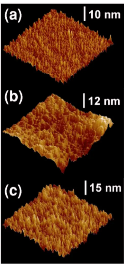
To study surface properties of the PSi samples photo-etched in HF/ FeCl3solution, we used ex situ AFM. In Fig.5, we show large-scale AFM images of the PSi samples photo-etched in a HF/ FeCl3 solution with共a兲 x=15 wt % for t=3 min and共b兲 x=15 wt % for t=5 min, together with that ob-tained by stain etching in 共c兲 x=47 wt % solution for t = 1 min.
In Fig. 5共a兲, the AFM image reveals many irregularly shaped hillocks and voids distributed randomly over the en-tire surface. The root-mean-square共rms兲 roughness obtained from this image is⬃1.0 nm. The lateral microstructures ob-served are on the order of 20⫺100 nm. In Fig. 5共b兲, many elongated oval shapes can be found and their lateral sizes are much larger than those in Fig. 5共a兲. The rms roughness in Fig.5共b兲 is ⬃2.4 nm. We also observed AFM images from samples photoetched in the 15 wt % solution for t = 0.5 and 1
min. The corresponding rms roughness is 0.6 共t=0.5 min兲 and 0.8 nm共1 min兲. It is thus considered that the rms rough-ness increases with increasing photoetching time t. The stain etched sample关Fig.5共c兲兴 shows AMF figures that are essen-tially the same as seen in Fig.5共b兲. The rms roughness ob-tained from Fig.5共c兲is⬃2.0 nm, slightly smaller than that in Fig.5共b兲.
If the porous size is truly on the order of 20⫺100 nm, the electronic states in such macroscopic pores are not quan-tum confined. We must note, however, that the nanocrystal-line sizes in the walls of the pores are important for quantum confinement effects. The nanocrystalline size may be related to the thickness of the pore walls, but not to the lateral pore size. Due to tip convolution, an accurate nanocrystalline size determination is impossible in AFM measurement. For stained PSi samples,8 the dimensions of most pits were re-ported to be in the range of⬃200−400 nm, which are much larger than the sizes required to induce quantum confinement effects, but the stained samples emitted visible lights. Re-cently, we carried out scanning electron microscopy mea-surements on stain etched PSi in a HF/ K2Cr2O7solution and observed nanocrystalline lumps of less than 10 nm on the macroscopic pores.
AFM and transmission electron microscopy images showed that the anodized and stained PSi showed a “fractal-FIG. 4. Etching time dependence of共a兲 PL emission intensity, 共b兲 PL peak
energy, and 共c兲 porous layer thickness formed in HF/FeCl3 solution共x
= 15 wt %兲.
FIG. 5. 共Color online兲 Large-scale 共1m⫻1m兲 AFM images of the PSi samples photoetched in HF/ FeCl3solution with共a兲 x=15 wt % for t=3 min
and共b兲 x=15 wt % for t=5 min, together with that obtained by stain etching in共c兲 x=47 wt % solution for t=1 min.
type” surface morphology.23 It is, thus, possible to consider that the nanocrystalline silicon enables the nondirect optical transition via a relaxation of the momentum conservation at energies well above the indirect-absorption edge, resulting in a supraband gap 共Eg
X兲 emission in the visible spectrum re-gion. Such a supraband gap emission has been clearly ob-served in porous GaP.24
C. Fourier-transform infrared spectroscopy
To further survey the origin of the visible emission in the HF/ FeCl3-prepared PSi, we performed FTIR measurements at room temperature. Figure 6 shows FTIR spectra of 共a兲 as-degreased crystalline silicon, 共b兲 HF/FeCl3-prepared PSi by stain etching 共47 wt %, 1 min兲, 共c兲 HF/FeCl3-prepared PSi by photoetching 共15 wt %, 3 min兲, and 共d兲 HF/ FeCl3-prepared PSi by photoetching共15 wt %, 20 min兲. The FTIR spectrum of the as-degreased crystalline sili-con 关Fig. 6共a兲兴 exhibits strong absorption peak near
614 cm−1. This peak is due to the lattice absorption band 共Si–Si兲. The peak at ⬃1107 cm−1can be assigned to the bulk Si–O–Si mode. Weak absorption shoulders are observed at ⬃1067 and ⬃1150 cm−1in the stain etched PSi sample关Fig.
6共b兲兴. These absorptions grow large as photoetching time
in-creases in the 15 wt % solution 关Figs. 6共c兲 and 6共d兲兴. The absorptions at ⬃1067 and ⬃1150 cm−1 are assigned to the transverse optical phonons in thin SiOxlayer and to the Si–O stretching mode, respectively.25
It is noted that the PSi samples passively etched in HF solution still emitted light in the visible region, but its strength becomes very weak. We, therefore, consider that the light emission observed in the HF/ FeCl3-prepared PSi sample is not arising from any oxide or its related centers. It is suggested that the surface oxide acts as a good passivation film and gives rise to an efficient emission at the PSi/oxide interface.26,27 We must note, however, that the surface of freshly etched PSi is almost totally covered by SiHxgroups. It has been reported that it is difficult to establish a direct
correlation between the visible luminescence properties in PSi and any particular chemical species, such as hydrides, oxide, or siloxene.28
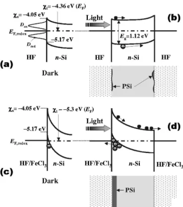
We finally present in Fig.7 the schematic energy-band diagrams for n-Si electrodes in pure HF 共pH=2.3兲 and HF/ FeCl3solutions without and with light illumination.29,30 The electron affinity s for silicon is ⫺4.05 eV.
31
The pure HF solution has a pH value of 2.3. Then, the electron energy of the pure HF solution with respect to vacuum is⫺4.36 eV 共l兲.32After immersion of the silicon substrate into the elec-trolyte in the dark, the Fermi levels EFand EF, redox on both sides of the n-Si/electrolyte interface are brought to be the same energy level by a transfer of electrons from the silicon substrate into the electrolyte关Fig.7共a兲兴.
The half-reaction for oxidizing agent FeCl3is33
Fe3++ e−= Fe2+ 共Eo= 0.771 V兲, 共1兲 where e− represents the electron and Eo is the standard re-duction potential in respect to the standard hydrogen elec-trode. Then, the redox potential Eabson the vacuum scale of the HF/ FeCl3redox system is then given by
Eabs= − 4.5 − Eo⬃ − 5.3 eV. 共2兲
Note that the larger the Eo value in the positive 共negative兲 sign, the stronger the oxidation 共reduction兲 agent. It is thus understood that the HF/ FeCl3 solution is more oxidative than the HF solution. The corresponding energy-band scheme is schematically shown in Fig.7共c兲.
The energy-band diagrams shown in Figs.7共a兲and7共c兲 have some similarities to that of the Schottky contact char-acterized by a metal/semiconductor interface. The photoex-FIG. 6. FTIR spectra of 共a兲 as-degreased crystalline silicon, 共b兲
HF/ FeCl3-prepared PSi by stain etching 共47 wt %, 1 min兲, 共c兲
HF/ FeCl3-prepared PSi by photoetching 共15 wt %, 3 min兲, and 共d兲 HF/ FeCl3-prepared PSi by photoetching共15 wt %, 20 min兲.
FIG. 7. Energy-band diagrams for n-Si immersed in pure HF solution关共a兲 and共b兲兴 and those in HF/FeCl3solution关共c兲 and 共d兲兴. In 共b兲, PSi is formed stably on the backside in opposition to the illuminated surface. In共d兲, PSi is formed on the illuminated surface.
cited electrons and holes are separated by the electric field in the surface space-charge layer, with the electrons and holes drifting into the opposite directions. The holes at the electrolyte/n-Si interface can participate in PSi formation. In Fig.7共b兲, however, the photoexcited holes can suffer to drift toward the surface due to the very small downward band bending or, possibly, due to the nearly flatband. Thus, no efficient PSi formation can be expected in the pure HF solu-tion. If wafer is dipped in the HF/ FeCl3solution关Fig.7共d兲兴, on the other hand, a large number of photoexcited holes move toward the electrolyte/n-Si interface at the front sur-face, resulting in the formation of PSi with good reproduc-ibility. The electrons arrived at the backsurface can be used in the reduction of FeCl3. This should be the main reason that the PSi formation is accelerated in the existence of FeCl3 in the HF solution. The effects of adding oxidizing agents, including FeCl3, in various fluoride solutions on the kinetics of PSi formation with and without light illumination have been discussed in more detail in Refs.7 and8.
Andersen et al.34 suggested that the preexisting state of the silicon surface plays a decisive role in determining PSi formation. They reported that cleaning the samples with or-ganic solvents prior to treating then with HF did not improve the outcome, but pretreating a sample with aqueous KOH solution resulted in formation of PSi during the subsequent treatment with HF combined with He–Ne laser illumination. However, no PSi layer was observed for samples treated less than 1 h in KOH. In all cases, the PSi spot on the front surface showed poor or no PL. Surprisingly enough, how-ever, the PSi was formed on that surface of the sample, which was not exposed with illumination, i.e., on the back-side. On the backside of all samples treatedⱖ1 h in KOH, a dark spot became visible and increased its size with increas-ing time in KOH. Uniform visible PL was observed from all of the spots on the backsurface.34
More recently, Koker and Kolasinski8suggested that hy-drocarbon contamination is one contributor to this type of abnormality. They found that through cleaning of the silicon wafer as well as the apparatus with methanol and acetone in an ultrasonic bath minimizes the variability. The PSi forma-tion rate increased if the silicon wafer is left in aqueous HF solution for extended periods prior to light irradiation. This was particularly noticeable in 48% HF solution for which it took⬃1 h to reach a steady-state rate. They also suggested that the acceleration may be due to chemical etching of the silicon surface which causes surface microroughening.8
The HF/electrolyte/n-Si energy scheme in Fig.7共b兲 can successfully explain why PSi is sometimes formed on the backside in opposition to the illuminated surface, as was ob-served by Andersen et al.34In the HF/ FeCl3-electrolyte/n-Si scheme, the energy bands of n-Si are strongly bent down-ward, as shown in Fig.7共c兲. By illuminating light, the elec-trons and holes are generated in n-Si 关Fig. 7共d兲兴. Since an electric field exists across the space charge region at the electrolyte/n-Si interface, the electrons and holes are sepa-rated. Then, potentials across the space charge, and conse-quently the band bending, are reduced. A “large” number of
holes accumulated at the HF/ FeCl3-electrolyte/n-Si interface can be participated in forming PSi layer only on the front surface关Fig.7共d兲兴.
IV. CONCLUSIONS
It was shown that large PSi layers can be synthesized on n-type silicon by photoetching in HF solution with adding FeCl3 under Xe lamp illumination. The addition of FeCl3 into HF largely shortened PSi formation time from ⬃10–60 min to a few minutes. The PL spectra exhibited a broad peak at ⬃2.0 eV. The AFM image revealed many ir-regularly shaped pores and voids distributed randomly over the entire surface at shorter etching times and elongated oval shapes at longer times. The FTIR spectroscopy showed an appearance of the surface Si–O–Si stretching mode 共Si − O − Si兲 at ⬃1064 cm−1. This surface oxide was expected to act as a good passivation film and gives rise to an efficient emission at the PSi/oxide interface. The PSi formation mechanism could be simply explained with the aid of surface energy-band diagram of n-type silicon in the HF/ FeCl3 elec-trolyte.
ACKNOWLEDGMENTS
The authors would like to thank Professor T. Miyazaki and Professor S. Ozaki and S. Kido, K. Inoue, and S. So-dezawa for their experimental support and useful discussion. This work was supported in part by the Foundation for Tech-nology Promotion of Electronic Circuit Board.
1A. G. Cullis, L. T. Canham, and P. D. J. Calcott, J. Appl. Phys. 82, 909
共1997兲.
2S. Ossicini, L. Pavesi, and F. Priolo, Light Emitting Silicon for Micropho-tonics共Springer, Berlin, 2003兲.
3J. Sarathy et al., Appl. Phys. Lett. 60, 1532共1992兲.
4N. Noguchi and I. Suemune, Appl. Phys. Lett. 62, 1429共1993兲. 5N. Yamamoto and H. Takai, Jpn. J. Appl. Phys., Part 1 38, 5706共1999兲. 6N. Yamamoto and H. Takai, Thin Solid Films 359, 184共2000兲. 7L. Koker and K. W. Kolasinksi, J. Phys. Chem. B 105, 3864共2001兲. 8L. Koker and K. W. Kolasinksi, Phys. Chem. Chem. Phys. 2, 277共2000兲. 9S. Shih, K. H. Jung, T. Y. Hsieh, J. Sarathy, J. C. Campbell, and D. L.
Kwong, Appl. Phys. Lett. 60, 1863共1992兲.
10J. L. Coffer, S. C. Lilley, R. A. Martin, and L. A. Files-Sesler, J. Appl.
Phys. 74, 2094共1993兲.
11M. T. Kelly, J. K. M. Chun, and A. B. Bocarsly, Appl. Phys. Lett. 64, 1693
共1994兲.
12Ş. Kalem and M. Rosenbauer, Appl. Phys. Lett. 67, 2551共1995兲. 13M. J. Winton, S. D. Russell, J. A. Wolk, and R. Gronsky, Appl. Phys. Lett.
69, 4026共1996兲.
14M. Nahidi and K. W. Kolasinski, J. Electrochem. Soc. 153, C19共2006兲. 15V. Petrova-Koch, T. Muschik, A. Kux, B. K. Meyer, and F. Koch, Appl.
Phys. Lett. 61, 943共1992兲.
16T. Maruyama and S. Ohtani, Appl. Phys. Lett. 65, 1346共1994兲. 17B. R. Mehta, M. K. Sahay, L. K. Malhotra, D. K. Avasthi, and R. K. Soni,
Thin Solid Films 289, 95共1996兲.
18D. W. Cooke, R. E. Muenchausen, B. L. Bennett, L. G. Jacobsohn, and M.
Nastasi, J. Appl. Phys. 96, 197共2004兲.
19C. Peng, L. Tsybeskov, and P. M. Fauchet, Mater. Res. Soc. Symp. Proc. 283, 121共1993兲.
20M. B. Robinson, A. C. Dillon, and S. M. George, Mater. Res. Soc. Symp.
Proc. 283, 191共1993兲.
21P. C. Searson, Appl. Phys. Lett. 59, 832共1991兲.
22T. Hadjersi, E. S. Kooij, N. Yamamoto, K. Sakamaki, H. Takai, and N.
Gabouze, Phys. Status Solidi C 2, 3375共2005兲.
23T. George, M. S. Anderson, W. T. Pike, T. L. Lin, R. W. Fathauer, K. H.
24K. Tomioka and S. Adachi, J. Appl. Phys. 98, 073511共2005兲.
25M. Saadoun, B. Bessais, N. Mliki, M. Ferid, H. Ezzaouia, and R.
Benna-ceur, Appl. Surf. Sci. 210, 240共2003兲.
26K. Tsunoda, E. Ohashi, and S. Adachi, J. Appl. Phys. 94, 5613共2003兲. 27T. Maruyama and S. Ohtani, Appl. Phys. Lett. 65, 1346共1994兲. 28S. Banerjee, K. L. Narasimhan, and A. Sardesai, Phys. Rev. B 49, 2915
共1994兲.
29R. Memming, in Comprehensive Treatise of Electrochemistry, edited by B.
E. Conway, J. O’M. Bockris, E. Yeager, S. U. M. Khan, and R. E. White
共Plenum, New York, 1983兲, Vol. 7, p. 529.
30S. Adachi and T. Kubota, Electrochem. Solid-State Lett. 10, H39共2007兲. 31S. Adachi, Properties of Group-IV, III⫺V and II⫺VI Semiconductors
共Wiley, Chichester, 2005兲.
32H. Seidel, L. Csepregi, A. Heuberger, and H. Baumgärtel, J. Electrochem.
Soc. 137, 3612共1990兲.
33P. Vanýsek, in CRC Handbook of Chemistry and Physics, edited by D. R.
Lide共CRC, Boca Raton, 2001兲, p. 8.