INVITED PAPER
Special Section on Electronic DisplaysNumerical Modeling; Thickness Dependence of J-V Characteristic for Multi-Layered OLED Device
Sang-Gun LEE†a), Hong-Seok CHOI†, Chang-Wook HAN†, Seok-Jong LEE†, Yoon-Heung TAK†, andByung-Chul AHN†,Nonmembers
SUMMARY A numerical model of multi-layered organic light emitting diode (OLED) is presented in this paper. The current density-voltage (J- V) model for OLED was performed by using the injection-limited current and bulk-limited current. The mobility equation was based on the field dependent model, so called “Poole-Frenkel mobility model.” The accuracy of this simulation was represented by comparing to the experimental results with a variable of EML thickness of multi-layered OLED device. There are two hetero-junction models which should be dealt with in the simulation.
The Langevin recombination rate of electron and hole is also calculated through the device simulation.
key words:OLED, fitting parameter, J-V characteristics, device simulation
1. Introduction
The active matrix organic light emitting diode (AM-OLED) is attracting a great interest in the display industry, due to its low cost for large sized panel. However, compared with inorganic semiconductor LED, the carrier transportation in OLED is not clear yet and still being debated [1]. Therefore, the current density-voltage (J-V) equation has not been pre- sented clearly in textbooks or research papers. So, many OLED researchers want to find out accurate universal and theoreticalJ-V equation.
There are two ways ofJ-Vinterpretation; the empirical interpretation and the device simulation. The former just represents the relation between current and voltage, but it is not enough to interpret the physical meaning. On the other hand, the latter is based on the physical equations in which all the parameters have physical meaning, and is valuable for understanding operation principles in OLED. Therefore, the objective of this work is to explainJ-V characteristics, using device simulation for multi-layered OLED device.
In this study, firstly we extracted fitting parameters contributing to the electronic transport of hole-only device (HOD) and electron-only device (EOD), respectively. Next, using the extracted fitting parameters, we simulated J-V characteristic of double-layered and multi-layered OLED device with varied layer thicknesses. Finally, we calculated the Langevin recombination rate in the multi-layered (EML
=20 nm) OLED device.
Manuscript received February 27, 2012.
Manuscript revised June 8, 2012.
†The authors are with OLED Development Center, LG Dis- play, Paju-si, Gyeonggi-do, Korea.
a) E-mail: [email protected] DOI: 10.1587/transele.E95.C.1756
2. Electronic Conduction for Organic Device
2.1 Injection-Limited current (JILC)
Generally, the thermionic emission model has been used to represent the injection current from the metal to the organic material through the Schottky barrier. However, the concept is appropriate for inorganic semiconductors which have high mobility and long mean-free-path. In case of organic semi- conductors which have low mobility and short mean-free- path, the carrier injection should obey a diffusion model [2].
The following equation can be used to represent the injec- tion current from metal to organic semiconductor;
JILC=qμENexp −qφB
kT
exp qγ
kT
√E
(1) whereqis the elemental charge,μthe mobility,Ethe elec- tric field, N the density state, and φB the injection barrier height. The barrier lowered due to the image force is ex- pressed by the last term with the factorγ.
Assuming the Coulomb potential of a charged trap, the mobility in OLED which usually has field dependence is expressed by the Poole-Frenkel model, as follows;
μPF =μ0exp −qεa
kT
exp qβ
kT
√E
(2) whereμ0 is the temperature-independent pre-factor mobil- ity, εa the thermal-activation energy of the trapped carrier, andβ the Poole-Frenkel factor as a fitting parameter. By substituting this intoμof Eq. (1) and assumingE=V/Lover the whole layer, the following equations can be obtained;
JILC=qμ0NV L exp
⎡⎢⎢⎢⎢⎢
⎣−q(φB+εa)
kT +q(γ+β) kT
V
L
⎤⎥⎥⎥⎥⎥
⎦ (3)
This corresponds to theJ-V equation for the injection lim- ited current (JILC) at the interface between metal and organic layer.
2.2 Bulk-Limited Current (JBLC)
The other limitation of the current can occur in the bulk re- gion, due to the space-charge effect. The field-dependence mobility is given as follows [3];
xJBLC
μ0εε0= 2 β4 exp
β√
E β3E3/2−3β2E+6β√ E−6
(4) Copyright c2012 The Institute of Electronics, Information and Communication Engineers
where the initial field at x=0 is assumed to be zero. This assumption is valid when the injection barrier is low enough or the contact is Ohmic. In the equation, the electric field is function ofxand cannot be represent byV/L. To obtain the J-V relation, Eq. (4) must be integrated again onx. Under the condition ofβ√
E 1, the approximate expression can be obtained by neglecting the lower order terms as follows [4];
JBLC ≈2μ0εε0
β α3/2V3/2 L5/2 exp
⎛⎜⎜⎜⎜⎜
⎝β
αV L
⎞⎟⎟⎟⎟⎟
⎠ (5)
where the field is assumedα(V/L) at x = L. Theαis an adjusting parameter to fit electric field to the real value [5].
This is theJ-V equation for the bulk limited current (JBLC) with field dependent mobility.
2.3 Transition betweenJILCandJBLC
We obtainedJ-VEqs. (3) and (5), which are valid in differ- ent conditions whereJILC andJBLC are dominant, respec- tively. The J-V characteristics in organic semiconductor, however, must be consideredJILCandJBLCsimultaneously.
One of the simplest ways is that the total current density leads to equation as follows;
JT heoretical= JILC·JBLC
JILC+JBLC
(6) where the current is simply limited by the smaller current, JILC orJBLC. This equation can express transition between JILCandJBLCvery well.
2.4 Extraction of Fitting Parameters
When the electrical modeling is studied, there are a lot of unknown input parameters to be considered. The most im- portant ones are energy levels, charge mobility, width of density of states and trapping levels in each layer. So, we proposed an alternative method to determine electrical pa- rameters of organic materials. This method enables to au- tomatically extract certain material parameters from experi- mental data, and is useful to determine material parameters of unknown information of materials.
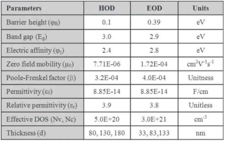
First, hole-only device (HOD) for hole transport layer (HTL) was fabricated with its thickness of 80, 130 and 180 nm. HOD consists of a single layer of HTL bewteen ITO anode and aluminum (Al) cathode.
Figure 1 shows comparison of J-V characteristics of the HOD between experimental data and fitting data in lin- ear and logarithmic scales ofJ. All experimental data must be simultaneously fitted by using Eq. (7). The fitting param- eters will minimize the difference between measured data and calculated data.
χ2= N
i=1
log
Jexp(V,d)
−log{Jtheoretical(V,d)}2
(7) whereN is the number of total experimental data points,
Fig. 1 Comparison ofJ-V characteristics in single-layered device be- tween experimental results (solid line) and fitting results (dashed line) as a variable of HTL thickness in linear scale (left) and logarithmic scale (right) of current density (J).
Table 1 Extracted parameters contributing to the electronic transport of single-layer devices.
V the voltage, d the layer thickness, Jexp the experimen- tally measured data points andJtheoreticalthe calculated data points using theoretical J-V equations (Eq. (6)). The rea- son why log Jis fitted instead ofJitself is to cover all the range of the current density varying in the order of 9. The χ2reflects the quality of the fit. The smallerχ2 shows the better agreement between experimental and calculated data.
Usually, theχ2 value below 1E-4 corresponds to very good fitting. Electronic conduction parameter of the electron-only device (EOD) for electron transport layer (ETL) was fitted by the same method as HOD.
Table 1 shows the parameters contributing to the elec- tronic transport of single-layer devices which were extracted from HOD for HTL and EOD for ETL, respectively, using Eq. (7). The extracted parameters not only represent thick- ness dependence of J-V characteristic but also have physi- cally meaningful results.
3. Comparison of Experimental Results and Device Simulations
We fabricated double-layered bipolar OLED device and multi-layered bipolar OLED device in order to demonstrate
Fig. 2 Energy diagram for double-layered OLED device.
our numerical modeling. We have simulated theJ-V char- acteristics of the devices by changing all parameter values related to the electrical conduction using 2-D device simu- lator, ATLAS (Silvaco Co.) in order to evaluate how each parameter affects the J-V characteristics. The simulation was performed based on the thermionic-emission-diffusion model for the carrier injection, and the Poole-Frenkel model for the field-dependent mobility, and hetero-junctions model for interface.
3.1 Double-Layered Bipolar OLED Device
Figure 2 shows a typical energy band diagram for a double- layered bipolar OLED composed of the ETL and HTL used in the simulation for EOD and HOD in the previous section.
The OLED device has an internal hetero-junction interface between HTL and ETL. We considered the thermionic emis- sion and field emission transport model [7], [8] at the inter- face between ETL and HTL for the simulation. The abrupt hetero-junction interface is taken into account on the basis of the one dimensional drift-diffusion formula. For instance, hole current density at the interface is represented by Eq. (8).
Jp=qνp(1+δ)
p+−p−exp −ΔEV
kT
(8) whereJp is the hole current density from HTL to ETL,νp
is hole thermal velocities, andΔEvis HOMO energy change going from HTL to ETL.p+andp−are hole current densi- ties at ETL and HTL, respectively. Theδparameter stands for the contribution due to thermionic field emission (tun- neling) and can be approximated as zero in our case.
The double-layered OLED device of light emission oc- curs in ETL since the internal energy-band offset for elec- trons was assumed to be much higher than that for holes.
Figure 3 shows the comparison of J-V characteristics between the results from device simulation and from ex- perimental data. The ETL thickness was fixed at 33 nm.
The experimental results of the double-layered OLED at the multiple thickness were simulated using the extracted HOD and EOD parameters. As shown in Fig. 3, a relatively good agreement between experimental results and simulated data as a variable of HTL thickness.
Fig. 3 Comparison ofJ-Vcharacteristics in double-layered OLED be- tween experimental results (solid line) and device simulation (dashed line) as a variable of HTL thickness in linear scale (left) and logarithmic scale (right) of current density (J).
Fig. 4 Energy diagram for multi-layered OLED device.
3.2 Multi-Layered Bipolar OLED Device
Figure 4 shows a typical energy band diagram for the multi- layered bipolar OLED composed of an ETL, an emitting layer (EML) including fluorescent host-dopant system, and an HTL, which are used in the experiment and simulation with a variable of doped EML thickness of 20, 70 and 120 nm.
Figure 5 shows the comparison of J-V characteristics between the results from device simulation and from exper- iment as a variable of doped EML thickness for the multi- layered bipolar OLED device. The multi-layered bipolar OLED device was simulated, using the extracted parameters of the bi-layered bipolar OLED. The simulation considered an interface trap model at the interfaces both HTL/EML and EML/ETL. In order to take into account EML materials in the simulation, we adopted a model of the equilibrium hop- ping transport in a doped disordered EML [9], [10], in which the density of state (DOS) of the dopant has Gaussian distri- bution, as shown in Eq. (9).
g(E)= Ni
√2πσi
exp
⎛⎜⎜⎜⎜⎝ E2 2σ2i
⎞⎟⎟⎟⎟⎠+ Nd
√2πσd
exp
⎛⎜⎜⎜⎜⎝−(E+Ed)2 2σ2d
⎞⎟⎟⎟⎟⎠ (9) whereNdare the total density of dopants,σdis the Gaussian
Fig. 5 Comparison ofJ-V characteristics in multi-layered OLED be- tween experimental results (solid line) and device simulation (dashed line) as a variable of HTL thickness in linear scale (left) and logarithmic scale (right) of current density (J).
Fig. 6 Langevin recombination rate of device at current density = 10 mA/cm2.
widths of the dopant DOS distributions, andEdis the energy shift between the intrinsic and doping states for traps:Ni= 2.1×017cm−3, σi =0.5 eV, Nd = 3.4×1018cm−3, σd = 0.3 eV.
As shown in Fig. 5, a relatively good agreement be- tween both results was obtained, except for the case of high current density. The deviation can be explained by the inac- curacy of the parameters such as the layer thickness, barrier height, or mobility. In the simulation on the various condi- tions of EML thickness, the same values were used for all the fitting parameters including barrier height and mobility.
However, such parameters can be easily varied, since it is hard to keep the same fabrication conditions for the differ- ent samples. In addition, it is also difficult to change the fitting parameters individually, as the parameters are closely related to one another in the simulation.
Figure 6 shows the calculated Langevin recombina- tion rate (LRR) in the multi-layered OLED device (EML
=20 nm). The rate becomes biggest at the interface be- tween HTL and EML, as the barrier for holes of HTL is much higher than that for the electrons of EML. So, using the device simulation, we could understand the various dis- tributions in this structure, such as the emission zone.
4. Conclusions
The parameters contributing to the electronic transport of HOD and EOD were extracted by the theoreticalJ-V equa- tions. The extracted parameters not only represent thickness dependence of J-V characteristic but also have physically meaningful results. The extracted parameters can explain various experimental results and be included into quantita- tive database of organic materials.
Next, we successfully simulated the double-layered bipolar OLED devices, using the extracted parameters of the HOD and EOD. We considered the thermionic emission and field emission transport model at the interface between ETL and HTL for double-layered OLED simulation. The sim- ulation successfully showed the agreement between exper- imental data and simulation results for the double-layered bipolar OLED devices with the varied HTL thickness.
Finally, we successfully simulated multi-layered OLED bipolar devices, considering the extracted parame- ters of double-layered OLED and the interface trap model at interfaces of HTL/EML and EML/ETL. The simulation successfully represented the agreement between experimen- tal data and simulation results for the multi-layered bipolar OLED device as a variable of doped EML thickness. Also, the simulation of multi-layered bipolar OLED device could inform us of the distribution of the recombination rate. The simulation of the J-V characteristics can help understand- ing the electrical-transport mechanism of OLED and will be very useful in explaining various experimental results.
References
[1] A. Loannidis, E. Forsythe, Yongli Gao, M.W. Wu, and E.M.
Conwell, “Current-voltage characteristic of organic light emitting diodes,” Appl. Phys. Lett., vol.72, no.23, pp.3038–3041, 1998.
[2] S.M. Sze, Physics of Semiconductor Device, 2nd ed., pp.254–270, Wiley New York, 1981.
[3] P.N. Murgatroyd and H.H. Wills, Theory of space-charge-limited current enhanced by Frenkel effect, J. PHYS.D: Appl. Phys., vol.3 pp.151–156, 1969.
[4] S.G. Lee and R. Hattori, “Current density equations representing the transition between the injection-limited and bulk-limited currents for organic semiconductors,” J. Information Display, vol.3, pp.72–76, 2009.
[5] R. Hattori and S.G. Lee, “Theoretical equations for current-voltage characteristics,” OLED SPIE Proceedings Series, pp.77–82, 2009.
[6] C.M. Wu and E.S. Yang, “Carrier transport across heterojunction interface,” Solid-State Electronics, vol.22, pp.241–248 1979.
[7] K. Yang, J. East, and G. Haddad, “Numerical modeling of abrupt heterojunctions using a thermionic-field emission boundary condi- tion,” Solid-State Electronics, vol.36, no.3, pp.321–330, 1993.
[8] C.M. Wu and E.S. Yang, “Carrier transport across heterojunction interfaces,” Solid-State Electronics 22, pp.241–248, 1979.
[9] V.I. Arkhipov, P. Heremans, E.V. Emelianova, G.J. Adriaenssens, and H. Bassler, “Charge carrier mobility in doping disordered or- ganic semiconductors,” J. Non-Crystalline Solids, vol.338, pp.603–
606, 2004
[10] V.I. Arkhipov, P. Heremans, E.V. Emelianova, G.J. Adriaenssens, and H. Bassler, “Charge carrier mobility in doped semiconducting polymers,” Appl. Phys. Lett., vol.82, no.19, pp.3245–3247, 2003.
Sang-Gun Lee is a Senior Research Engi- neer at LG Display, OLED Business, Paju, Ko- rea. He received the B.S. degree in physics from Kookmin University, Seoul, Korea, in 2002, the M.S. degree in physics from Yonsei University, Seoul, Korea, in 2005. He received the Ph.D.
degree in electrical engineering from Kyushu University, Fukuoka, Japan, in 2010 research- ing physics-based OLED analog behavior mod- eling. He joined LG Display in 2010. Now, he is responsible for research on WOLED as research engineer and has worked on OLED device modeling and mechanism at OLED Technology Team 2, OLED Business, LG Display.
Hong-Seok Choi is a Chief Research Engi- neer at LG Display, OLED Business, Paju, Ko- rea. He obtained his B.S., M.S., and Ph.D. de- grees in physics from Seoul National Univer- sity, Korea, in 1992, 1994, and 1999, respec- tively. His Ph.D. work was on optical properties of transition metal oxides. In 2001, he joined LG Electronics Co. and worked on technical de- velopment of OLED. In 2008, he transferred to LG Display and has researched OLED as a Part Leader at OLED Technology Team 2, OLED Business, LG Display.
Chang-Wook Han is a Research Fellow at LG Display, OLED Business, Paju, Korea.
He obtained his B.S. and M.S. degrees in mate- rial science from Seoul National University, Ko- rea, in 1987 and 1989, respectively. He also re- ceived his Ph.D. in electrical engineering from Seoul National University in 2007, researching a-Si TFTs and the pixel structure of AMOLEDs on a flexible metal substrate. Since joining LG Display in 1990, he has worked on the device and process development of TFT backplanes for AMLCDs and also on the TFT backplane, circuit, and panel structure of AMOLEDs. Now, he is responsible for research on AMOLEDs as a Team Leader at OLED Technology Team 2, OLED Business, LG Display.
Seok-Jong Lee is a Research Fellow at LG Display, OLED Business, Paju, Korea. He ob- tained his M.S. and Ph.D. Degrees in Organic Chemistry from Pohang University of Science and Technology, Korea, in 1991 and 1995, re- spectively. His Ph.D. work was on the total syn- thesis of Natural Product, (+)-Xestospongin A.
From 2001 to 2005, he joined the Samung SDI and had worked on the development of OLED device and OLED material. In 2005, he joined the LG Display and since then he has worked on the development of OLED device for AMOLED displays. Now, he is re- sponsible for OLED device research on AMOLEDs as a Team Leader at OLED Technology Team 1, OLED Business, LG Display.
Yoon-Heung Tak is a Vice President at LG Display, OLED Business, Paju, Korea. He is responsible for the research and development of AMOLED displays. He obtained his B.S.
degree in chemistry and M.S. degree and his Ph.D. in physical chemistry from Philips Mar- burg University, Germany, in 1991, 1994, and 1997, respectively. His Ph.D. work was on the injection, transport, and recombination of charge carriers in OLEDs. In 1997, he joined the LG Electronics Co. and since then he has worked on the technology, process, and product development of AMOLED displays. He is currently the Vice President of the OLED Technology De- velopment Division, OLED Business, LG Display.
Byung-Chul Ahn is a Senior Vice President at LG Display, OLED Business, Paju, Korea. He is responsible for OLED technology and prod- uct development. He obtained his B.S. degree in metallurgy from Yonsei university, Seoul, Ko- rea, in 1978. He also obtained his M.S. degree in metallurgy from Seoul National University, Ko- rea, in 1981. He also received Ph.D. degree in the physics of the electron from Tokyo Institute of Technology, Japan, in 1997. He joined LG Electronics Co. in 1984 and he worked on the research and development of LCD. Since joining LG Display in 1999, he worked on the technology and development of next generation display. He has been working on the research and development of OLED since 2008.
He is currently the Head of the OLED Development Center, OLED Busi- ness, LG Display.