INVITED PAPER
Special Section on Recent Development of Electro-Mechanical Devices (IS-EMD2012)The Contact Resistance Performance of Gold Coated
Carbon-Nanotube Surfaces under Low Current Switching
John W. McBRIDE†a), Chamaporn CHIANRABUTRA††, Liudi JIANG††,andSuan Hui PU†,Nonmembers
SUMMARY Multi-Walled CNT (MWCNT) are synthesized on a sil- icon wafer and sputter coated with a gold film. The planar surfaces are mounted on the tip of a piezo-electric actuator and mated with a gold coated hemispherical surface to form an electrical contact. These switching con- tacts are tested under conditions typical of MEMS relay applications; 4 V, with a static contact force of 1 mN, at a low current between 20–50 mA.
The failure of the switch is identified by the evolution of contact resistance which is monitored throughout the switching cycles. The results show that the contact resistance can be stable for up to 120 million switching cy- cles, which are 106orders of higher than state-of-the-art pure gold contact.
Bouncing behavior was also observed in each switching cycle. The failing mechanism was also studied in relation to the contact surface changes. It was observed that the contact surfaces undergo a transfer process over the switching life time, ultimately leading to switching failure the number of bounces is also related to the fine transfer failure mechanism.
key words: carbon nanotubes, contact surface, MEMS switching surface, fine transfer mechanism, contact resistance
1. Introduction
In MEMS relay devices, a stable contact resistance (Rc) of less than 1–2Ω is required over millions of switching cy- cles [1]. To meet this specification a number of materials have been used for the switch contact surfaces, for example palladium alloys, platinum alloys, and gold [1]. Although these materials have low electrical resistivity, they are soft and prone to wear. Silicon carbide and diamond have also been investigated because of high elastic moduli, but these materials have unsuitably high resistivities.
Carbon nanotubes (CNTs) have both good electrical and mechanical properties [2], making them attractive for contact surfaces for a wide range of applications, includ- ing MEMS relays. CNTs have two main structures: single- walled nanotubes (SWCNTs) and multi-walled nanotubes (MWCNTs). MWCNTs are relatively easy to grow with controlled a length, diameter and density [3]–[5]. Elec- trical contact applications of structured (vertically aligned) MWCNTs was first investigated in [6], where the contact resistances of an Au-Au contact pair (Au hemispherical ball and Au substrate) and an Au-MWCNT contact pair (Au hemispherical ball and MWCNT substrate) have been com-
Manuscript received January 7, 2013.
Manuscript revised April 16, 2013.
†The authors are with University of Southampton Malaysia Campus, Johor, 79200, Malaysia.
††The authors are with the Faculty of Engineering and the En- vironment, University of Southampton, Southampton SO17 1BJ, UK.
a) E-mail: [email protected] DOI: 10.1587/transele.E96.C.1097
pared. They found that the contact resistance of the Au- MWCNT contact pair was higher (∼108Ω) than that of the Au-Au contact pair (∼0.58Ω) [6]–[9] due to the nonconduc- tive substrate on which MWCNT are grown. The substrate inhibits the current travelling along the MWCNTs; only lat- eral conduction is possible between the MWCNTs, resulting in higher contact resistance. To improve the performance an Au-coated MWCNT surface (Au/MWCNT) was devel- oped [6]–[15]. Results show that by using the Au/MWCNT surface, Rc∼0.68Ωand much improved life cycles of the switch (i.e. 70 million cycles for a current of 20 mA) can be achieved with CNTs of 50µm height, demonstrating great potential for switch contact applications. It was observed that material transfer was always from the Au/MWCNT substrate (anode) to the Au ball (cathode) [11]–[13]. Fur- thermore, at a current of 20 mA, a fine transfer process dom- inated [12]–[15]. The fine transfer process is described as a thermal process associated with the softening and melting of asperities during contact opening and is described in detail in [12]. From this work a simplified fine transfer model was defined and used to predict failure at different current levels other than the 20 mA used to define the model. It has since been shown that the wear process is a combination of both fine transfer and a delamination mechanism [12]–[15]. Thus the determination of the failure behavior of Au/MWCNT films has not yet been defined. In this work, four stages of the contact resistance and the bouncing behavior will be introduced to analyze characteristic failure processes. Evo- lution of contact resistance and the number of bounces are studied throughout the switching cycles, and the failure of the switch is identified by the sharp increase of contact re- sistance. The paper also re-examines the effect of the fine transfer mechanism based on the thermal model.
2. Material Preparation
The switch consists of two surfaces which are classified ac- cording to the direction of the DC electric current. The cath- ode is a 2 mm diameter stainless steel hemispherical ball sputter coated with a 10 nm thick Cr as adhesion layer fol- lowed by a 500 nm thick Au. This Au coated ball has a surface roughness, Ra of 92 nm. The anode is a silicon wafer with vertically aligned MWCNTs on top which has been sputtered coated with a 500 nm thick Au layer. This Au/MWCNT surface has a surface roughness of 1.3µm.
The growth process of the vertically aligned MWCNT is di- vided into three processes: cleaning, sputtering and growing Copyright c2013 The Institute of Electronics, Information and Communication Engineers
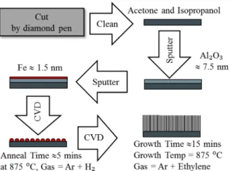
Fig. 1 CNTs growth apparatus and procedure.
Fig. 2 Dense forest of MWCNT.
as shown in Fig. 1.
The cleaning process consists of submerging and soni- ficating the silicon wafers (7 mm by 2 mm) for 20 minutes in acetone and isopropanol, respectively. The clean substrate is then coated with 7.5 nm thick Al2O3 buffer layer followed by a 1.5 nm thick Fe catalyst layer. The final growth of the MWCNTs is accomplished by chemical vapor deposi- tion (CVD) in a furnace. A mixture of Ar and H2gases is introduced into the chamber which is heated to 875◦C. At this step, the substrate is annealed at this temperature for 5 minutes. The anneal step is needed to create Fe islands.
These islands act as the seeds for MWCNT to grow. After the substrate is annealed, a mixture of ethylene (C2H4), H2
and Ar is passed through the chamber at 875◦C for 15 min- utes to enable the growth of MWCNTs with height of ap- proximately 30µm. A cross-section SEM image of the ob- tained MWCNT forest is shown in Fig. 2. It was observed that the MWCNT substrate was well-aligned and uniform across the entire substrate.
Following the growth of MWCNTs, a final step is to sputter 500 nm thick Au layer on the MWCNTs to obtain the Au/MWCNTs surface. The resulting surface has a rough- ness (Ra) of 1.3µm and the penetration depth of Au into the MWCNTs is approximately 1µm as shown in Fig. 3.
Fig. 3 Au/MWCNT composite contact.
Fig. 4 The schematic of the test configuration.
3. Methodology
To simulate the repeated switching action of a MEMS relay, the Au/MWCNTs substrate is attached to a PZT cantilever.
The test platform consists of the PZT with the Au/MWCNT substrate as anode while the Au-coated hemispherical sur- face at the top is the cathode. The setup configuration is shown in Fig. 4. The platform is mounted on an anti- vibration workstation in a temperature controlled room.
A dynamic contact force of 1 mN is set for the exper- iment. This dynamic force was measured using a Kistler (type: 9207) force sensor mounted above the ball contact as shown in Fig. 4. The contact force was generated by PZT cantilever which was actuated at frequency of 1 Hz. The data in Fig. 5 shows a typical result of the impact force of the two switching contacts, followed by a stabilization of the 1 mN contact force after 0.2 s.
To measure the contact gap between the contacts, dur- ing the open part of a cycle, a laser system was used. This measured the displacement of the PZT cantilever. With no contact, the cantilever could vibrate freely with a maximum displacement of approximately 40µm. When exerting a contact force of 1 mN on the contacts this displacement (i.e.
the contact gap) becomes 2µm.
Fig. 5 Measured contact force with 1 Hz activation of PZT actuator.
Fig. 6 The location of the experimental positions for the 4 current levels (20, 30, 40 and 50 mA) on the Au/MWCNT substrate.
The experiments were conducted with currents of 20, 30, 40 and 50 mA, a load voltage of 4 V, and a nominal con- tact force 1 mN. As shown in Fig. 2, the MWCNT forest is uniform over the whole testing substrate. All tests using dif- ferent current levels were conducted on the same substrate with different positions as shown in Fig. 6. A signal func- tion generator with voltage amplification was used to actuate the PZT cantilever at 20 V at a frequency range of 1100 Hz.
Testing is performed as follows:
• Apply voltage to vibrate PZT cantilever by the function generator at testing frequency (ftest).
• Record the number of bounces (Bc).
• Measure and record the contact resistance (Rc) and the number of bounces at the 10th, 100th, 1000th, 10000th, and 100,000th cycles, and then every 12 hours until the contact fails. Record time to failure (ttest).
For the experiment operated at 20 mA, ftestwas 30 Hz. For 30–50 mA, the ftest was set up at 100 Hz to reduce testing time. Therefore, the numbers of operations (Ntest, cycles) are derived from;
Ntest=ttest×ftest (1)
As shown in Fig. 5, the impacting force (1 mN) from the PZT cantilever will be stable after the contact is closed for 0.2 seconds. Therefore, to measure Bc, ftesthas to be de- creased to 1 Hz before counting to get the complete bounce process. The contact resistance Rcis measured using 4-wire measurement method. While measuring Rc, the experiment
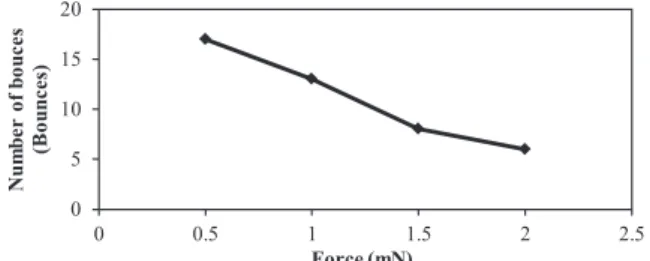
Fig. 7 The number of bouncing versus force for Au-Au/MWCNT, load voltage 4 V and load current 20 mA.
Fig. 8 Contact resistance against number of cycles for Au-Au/MWCNT contact pair with currents of 20–50 mA, 4 V.
is paused for 5 minutes to allow for the resistance to stabi- lize.
4. Results
4.1 Relationship between Number of Bounces and Force The bouncing behavior has been observed during a closing process, [13]–[15]. Before investigating the failure behav- ior, the relationship between the number of bounces and force were studied on a contact sample which consists of a Au ball and an Au/MWCNT surface with 50µm CNTs in height. The static contact forces varied between 0.5 mN and 2 mN. The number of bounces for each force is shown in Fig. 7, 17 bounces occurred at 0.5 mN and gradually de- creased to 6 bounces at 2 mN.
4.2 Contact Resistance against the Number of Cycles The contact resistance against the number of cycles is shown in Fig. 8. The contact resistance behavior is similar across all values of current and can be described in four stages. The first stage is an unstable stage of Rc. The Rc starts below 0.4Ωand decreased over the first 5,000 cycles. The second stage where there is gradual low level increase in Rc over millions of switching cycles. In the third stage there is a rapid increase in Rc. The final stage is when the resistance has reached a failure point, this is defined here as three times the nominal resistance, (1.5Ω).
Fig. 9 The number of bounce against number of cycles for Au- Au/MWCNT contact pair with currents of 20–50 mA, 4 V.
4.3 The Number of Bounces against the Number of Cycles The number of bounces against the number of cycles is shown in Fig. 9, for the 4 current levels. As with the Rc behavior, the change in bounces can be divided into four stages. The first stage of Bcis an unstable stage. Bcstarts at between 3-5 bounces except the experiment operated at 50 mA for which Bcis 12. The bounce process is a complex interaction of components. After performing switching for 5,000 cycles, Bcdecreases to 1-4 bounces. This is the sta- ble stage of Bc, which remains stable for millions of cycles, with a gradual increase in the number of bounces for this period. Then the switching contact shifts to the rising stage of Bc. In this stage, Bcrises sharply. Finally, the contact is in the failure stage and Bcshows a reduction, indicating that the contact has failed.
5. Discussion
The data from Fig. 8 and Fig. 9 is used to obtain the numbers of cycles (Ntest) to failure of the experiment at currents of 20, 30, 40 and 50 mA as shown in Table 1. These are defined as the number of cycles when R=1.5Ω.
Figure 10, shows the numbers of cycles to failure (Ntest) for the 4 current levels used. The data is superimposed for comparison with data from the fine transfer model, and from previous experimental data [12]. The difference in failure cycles and the significant improvement at the higher cur- rent levels is a direct consequence of the additional Cr layer under the Au surface on the ball. The fine transfer model in [12] was based on a single (20 mA) data point, thus although the trend is correct there is an offset between the current data and the model.
Since the trends of Rcand Bcwith current are similar, the data for 30 mA, 4 V (1 mN) is chosen to show the graph appearance of the four stages of the failure. These four stages; namely unstable, stable, rising and failure stages, are shown in Fig. 11.
The first stage is the unstable stage. In Fig. 12, the decreasing trend of both contact resistance and number of
Fig. 10 The number of cycle to failure for a given load current. Dots on solid line resulted from [12]. Dotted line is predicted data from fine transfer model [12]. Dots on dashed line are the Ntest.
Fig. 11 Four stages of the contact resistance and the number of bounces behavior.
Fig. 12 The unstable stages of the failure behavior.
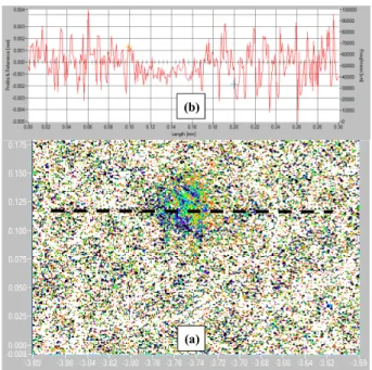
Fig. 13 (a) 3D surface profile of anode surface, 301X301 data points over area 0.3×0.3 mm. of Au-Au/MWCNT; 30µm height, (b) Surface profile of Au-Au/MWCNT composite surface.
Fig. 14 The stable stage.
bounce is shown. Based on the observation, this perma- nent deformation process of the Au/MWCNT substrate with 30µm MWCNT is completely finished within 5,000 switch- ing cycles.
To investigate the wear-in period further, the Au- Au/MWCNT contact pair was tested for around 5,000 cy- cles with a current of 30 mA, 4 V (1 mN). After which a laser profiler was used to scan the Au/MWCNT surface (Fig. 13(a)) to investigate the crater of the MWCNT de- formation, as shown in Fig. 13(b). It is possible that the MWCNT may have buckled permanently when the contact force was greater than a load threshold, resulting in plastic deformation.
The stable stage is plotted over 60 Million cycles and shows a small increase in the number of bounces, and a sta- ble contact resistance. Rcand Bcare stable within the small ranges (±0.05Ωfor Rcand 4-8 bounces for Bc) as shown in Fig. 14. At this stage, the fine transfer mechanism is the dominant transfer process. The Au layer is gradually re-
Fig. 15 Au layer transfer at 1 million cycles at 30 mA (yet to fail) on the Au/MWCNT surface, 30µm height.
Fig. 16 Material transfer observed at 27th million cycle, at 30 mA (yet to fail) on the Au/MWCNT surface; 30µm height.
moved from Au/MWCNT (anode) to Au probe (cathode).
This leads to a gradually change in the contact surface. To confirm this, an experiment with Au-Au/MWCNT surface of 30µm height, with a current of 30 mA, 4 V (1 mN) was tested for around 1 million cycles. SEM image taken from the contact surface is shown in Fig. 15. It can be observed that Au layer on the Au/MWCNT surface is starting to de- plete and transfer to the Au ball.
When the switching contact is in the rising stage, the contact resistance and number of bounces continues to rise, albeit with a steeper gradient. The depleted surface causes the increase in contact resistance due to the decrease in the metallic contact area. Previously the current passes through the Au asperities at the center of the surface. When the cen- ter area does not have any Au surface remaining because of the material transfer process, the current density will travel through the area surrounding center until the contact is com- pletely worn out (i.e. contact failure). To illustrate this pro- cess, the same experiment was tested to 27 million cycles.
Then the SEM was used to examine the contact surface as shown in Fig. 16. The Au layer is completely depleted at the center as shown by the black area. Therefore, the conductive area supporting the current density is significantly reduced and the current starts to move via the area around it depleted
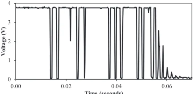
Fig. 17 The bounce process at the highest point on the rising stage.
Fig. 18 Au/MWCNT surface at 49 million cycles (failed contact) tested at current of 30 mA.
area. (Grey shaded area).
In Fig. 16, the MWCNT layer is exposed in the black area. It is known that CNTs have high elastic moduli [2], [3] and so the number of bounces should increase with gold removal. The number of bounces increases sharply to the maximum number of bounces when the Au layer nearly completely worn out. The maximum bounce process is shown in Fig. 17.
The final stage is the failure stage of Rc, which shows the contact resistance rising rapidly. In this stage the con- tact surface is totally depleted as shown in Fig. 18, i.e. the contact area completely touches the MWCNT underneath.
The MWCNT surface causes the high contact resistance of this last stage. Therefore, the contact pairs are considered to have failed as the contact resistance is greater a magnitude of three times the nominal value [12], which in this case is about 1.5Ω.
The number of bounces drops rapidly in the failure stage to show that the contact has failed. At this stage, the number of bounces should be equal to the peak amount in the rising stage. However, since the contact surface is al- most totally depleted, some bounce events are not recorded as shown in Fig. 19 as the switch touches the non-conductive area which is entirely MWCNT.
In summary, it is possible to use contact resistance and the number of bounces to predict the failure of the switch
Fig. 19 The bounce process in the failure stage for Au-Au/MWCNT, 30µm height contact pair with current of 30 mA, 4 V (1 mN).
contact. A benefit of the results presented that it allows the trend of Bcto be used predicting when the contact is going to fail, i.e. when contact resistance or the number of bounces increase sharply.
6. Conclusion
It has been shown that a Au ball surface coupled with an Au/MWCNT (gold-coated multi-walled carbon nanotube structure) substrate, can withstand more than 49 million switching cycles at 50 mA (0.2 W), at a low contact force of 1 mN. This is a significant increase in current over previous published work on these surfaces. The contact resistance across the interface is used as the indicator for determining the failure modes of the contact switch. The following con- clusions are reached:
• The contact resistance trend is similar to previous studies, and remains stable for over 49 million switching cycles for all current levels between 20 and 50 mA.
• The mechanism of failure previously defined as fine trans- fer shows that the Au-MWCNT anode surface is losing material to the cathode ball.
• The contact bounce is affected by the changes in the sur- face and is correlated with the changes in Rc.
• The trend of number of bounces trend can be used to pre- dict the lifetime. If the contact resistance or the number of bounces starts to increase rapidly, the user can predict that the contact is going to fail in the near future.
References
[1] R.A. Coutu, Jr., et al., “Microswitches with sputtered Au, AuPd, Au on-AuPt, and AuPtCu alloy electric contacts,” Components and Packaging Technologies, vol.29, pp.341–349, 2006.
[2] M.S. Dresselhaus, G. Dresselhaus, and P. Avouris, Carbon Nan- otubes: Synthesis, Structure, Properties, and Applications, Springer, Berlin, 2001.
[3] A. Jorio, G. Dresselhaus, and M.S. Dresselhaus, Carbon Nanotubes:
Advanced Topics in the Synthesis, Structure, Properties and Appli- cations, Springer, 2008.
[4] V. Sgobba and D.M. Guldi, Carbon nanotubes-electronic/electro- chemical properties and application for nanoelectronics and photon- ics, Chemical Society Reviews, vol.38, pp.165–184, 2009.
[5] W. Maser, A.M. Benito, E. Munoz, and M.T. Martinez, Carbon Nan- otubes: From Fundamental Nanoscale Objects Towards Functional
Nanocomposites and Applications, Springer, Netherlands, 2008.
[6] E.M. Yunus, J.W. McBride, and S.M. Spearing, “The relationship between contact resistance and contact force on Au coated car- bon nanotube surfaces,” 53rd IEEE Holm Conference on Electri- cal Contacts, USA, Institute of Electrical and Electronics Engineers, pp.167–74, 2007.
[7] E.M. Yunus, J.W. McBride, and S.M. Spearing, “Improving the con- tact resistance at low force using gold coated carbon nanotube sur- faces,” 24th International conference on electrical contact pp.507–
13, St Malo, France, 2008.
[8] E.M. Yunus, J.W. McBride, and S.M. Spearing, “Investigation of gold sputter coated vertically aligned multi-walled carbon nanotubes for RF MEMS contact surfaces,” Material Research Society Meet- ing, Fall Meeting Symposium GG., Warrendale, USA, 2008.
[9] E.M. Yunus, J.W. McBride, and S.M. Spearing, “The relationship between contact resistance and contact force on Au coated carbon nanotube surfaces under low force conditions,” Components and Packaging Technologies, pp.650–657, 2009.
[10] E.M. Yunus, J.W. McBride, and S.M. Spearing, “Improving the con- tact resistance at low force using gold coated carbon nanotube sur- faces,” European Physical Journal - Applied Physics, vol.50, no.1, pp.12904–12909, 2010.
[11] E.M. Yunus, J.W. McBride, and S.M. Spearing, “Low force electri- cal switching using gold coated vertically aligned multi-walled car- bon nanotubes surfaces,” IEICE Technical Report, pp.61–64, 2008.
[12] J.W. McBride, “The wear processes of gold coated multi-walled car- bon nanotube surfaces used as electrical contacts for micro-electro- mechanical switching,” Nanoscience and Nanotechnology Letters, vol.2, no.4, pp.357–361, 2010.
[13] J.W. McBride, E.M. Yunus, and S.M. Spearing, “Gold coated multi- walled carbon nanotube surfaces as low force electrical contacts for MEMS devices: Part 1,” Proc. 55th IEEE Holm Conference on Elec- trical Contacts, pp.281–87, Minneapolis, USA, 2009.
[14] J.W. McBride, S.M. Spearing, L. Jiang, and C. Chianrabutra, “Gold coated carbon-nanotube surfaces as low force electrical contacts for MEMS devices: Part II, fine transfer mechanisms,” 57th IEEE Holm Conference on Electrical Contacts Minneapolis, USA: Institute of Electrical and Electronics Engineers, pp.1–6, 2011.
[15] J.W. McBride, L. Jiang, and C. Chianrabutra, “Fine transfer in elec- trical switching contacts using gold coated carbon-nanotubes,” 26th International Conference on Electrical Contact, pp.353–58, Beijing, China, 2012.
[16] J.F. Llewellyn, The Physics of Electrical Contacts, Oxford Claren- don Press, 1957.
[17] R. Holm, Electric Contacts: Theory and Application, 4th ed., Springer, 1999.
John W. McBride is Professor of Electro- Mechanical Engineering in the School of Engi- neering Sciences at the University of Southamp- ton. He is chair of the Electro-Mechanical re- search group, and was previously Head of Re- search in the School (2001–2005). In 2006 he was awarded the IEEE Holm Scientific Achieve- ment award. His main research interests include Electrical Contacts, Metrology and Instrumenta- tion. Internationally he is associate editor of the IEEE Transactions CPMT and a member of the organizing committee for the IEEE Holm Conference on Electrical Con- tacts.
Chamaporn Chianrabutra received M.Eng. and B.Eng. in Mechanical Engineering from Kasetsart University, Thailand (2006) and King Mongkut’s Institute of Technology Lad- krabang (2001), Thailand, respectively. She has been working with Electrical-Mechanical Manufacturing Engineering Program (EMME), Kasetsart University (KU) since October 2008 as a Lecturer, Deputy Head of EMME and ad- ministration committee of Industrial Automa- tion Training Center. In 2006, she received a scholarship for her master degree from National Electronics and Computer Technology Center (NECTEC). She received her M.Eng. in Mechanical Engineering from Kasetsart University, Thailand in 2008. Currently, she is pursuing his Ph.D. in Engineering Sciences at the University of Southamp- ton.
Liudi Jiang was awarded her Ph.D. in 2002 by the University of Dundee for research in ad- vanced material physics. Subsequently (2002–
2005), she joined the Scottish Microelectronics Centre at the University of Edinburgh as a post- doctoral research fellow for the development of MEMS technologies for harsh environment ap- plications. She was appointed a RCUK Aca- demic Fellow (Roberts Fellow) in 2006 by the Engineering Material group at the University of Southampton, became a lecturer in 2008. Liudi is a member of The Institution of Engineering and Technology, a member of the Institute of Physics, and a Chartered Physicist.
Suan Hui Pu was awarded a Ph.D. in Micro- Electro-Mechanical Systems (MEMS) from Im- perial College London in 2010. He earned his MEng in mechanical engineering, also from Im- perial College London, in 2006. Suan-Hui has substantial experience in the development of MEMS devices and structures, including design, modelling, process development and character- isation. Prior to joining USMC, Suan-Hui was with Infineon Technologies, working on prod- uct yield enhancement in a 200 mm wafer fab.
Hence, he is keen to use his experience to help USMC students settle into their course. He is also happy to answer any queries they may have in re- lation to earning a degree from the University of Southampton, or about living in the UK.