Contents
ABSTRACT...I
Chapter 1 Introduction of electron holography...1
1.1 Transmission electron microscopy...1
1.2 Overview and history of electron holography ...2
1.3 Theoretical basis of off-axis electron holography...4
1.3.1 Hologram formation in off-axis electron holography...5
1.3.2 Hologram reconstruction ...7
1.3.3 Phase shift by magnetic and electric fields ...10
1.3.4 Applications of off-axis electron holography ...12
1.4 Other Forms of electron holography...13
1.5 Other techniques for phase measurement ...16
1.5.1 Phase measurement using the transport of intensity equation ...16
1.5.2 Phase measurement using Lorentz microscopy ...17
1.6 Aims and contents in this thesis ...19
Reference ...21
Chapter 2 Development of stage-scanning electron holography ...25
2.1 Introduction...25
2.2 Development of stage-scanning electron holography...26
2.2.1 Principle and experimental methods ...26
2.2.2 Results and discussion ...29
2.3 Stage-scanning electron holography with a digital aperture ...32
2.3.1 Methods...32
2.3.2 Results and disctssion ...33
2.4 Conclusions...35
Reference ...36
3.2 Improvement of stage-scanning electron holography for a non-phase object 39
3.2.1 Principle ...39
3.2.2 Experimental methods ...44
3.2.3 Results and discussion ...44
3.2.4 Drift effect of the biprism and specimen stage and considerations for recording ...50
3.3 Demonstration of resolution improvement in stage-scanning electron holography ...54
3.3.1 Experimental methods ...54
3.3.2 Results and discussion ...56
3.4 Conclusions...58
Reference ...60
Chapter 4 Super-resolution phase reconstruction technique in stage-scanning electron holography ...62
4.1 Introduction...62
4.2 Principle ...64
4.2.1 Scan step is a multiple of the CCD pixel size...65
4.2.2 Arbitrary scan step ...67
4.3 Simulation for super resolution electron holography...69
4.4 Experimental methods ...72
4.5 Results and discussion ...73
4.6 Fresnel diffraction effect ...75
4.7 Conclusions...77
Reference ...78
Chapter 5 Conclusions ...81
Acknowledgements...83
ABSTRACT
Electron holography is a powerful electron-interference technique through the use of transformation electron microscopes (TEMs). Contrary to the conventional TEM techniques, which record only the image intensity, electron holography yields both the phase and amplitude of the electron wave that passed through a specimen. The successful developments of field-emission electron guns and electron biprisms made electron holography a practical tool allowing quantitative and precise measurements. In recent research, off-axis electron holography is the most widely used holography technique. In this technique, Fourier transformation is commonly used for the phase-retrieval. However, the spatial resolution of the reconstructed phase image is limited by the fringe spacing of the hologram. Therefore, how to improve the spatial resolution of the reconstructed phase images becomes an important topic in electron holography field.
and significantly sharper images were obtained with the former technique.
In the stage-scanning electron holography, the step size is a key parameter during the stage scan. If the scanning step is a multiple of the CCD pixel size then the spatial resolution of the reconstructed phase image is determined by the CCD pixel size divided by magnification, or the microscope resolution. If the scanning step is an arbitrary, in which the holograms are recorded with sub-pixel specimen shifts, therefore these holograms provide different phase information. In this case, super-resolution reconstruction technique is introduced into stage-scanning electron holography. The processing of the acquired series of holograms with sub-pixel specimen shifts result in a higher pixel density and spatial resolution as compared to the phase image obtained with conventional holography. The final resolution exceeds the limit of the CCD pixel size divided by the magnification.
Chapter 1 Introduction of electron holography
1.1 Transmission electron microscopy
Transmission electron microscopy (TEM) has revolutionized our understanding of materials and introduces us into nano-world by completing the processing-structure-properties links down to atomistic levels [1-15]. TEM is powerful tool which can provide almost all the structural, phase, and crystallographic data and allow us to observe nanometer sized object [1].
In TEM, an electron beam of electrons is transmitted through an ultra-thin specimen. The transmitted electron beam interacts with the specimen. From the interaction between the electron beam and the specimen, an image is formed; the image is then magnified and focused by the electron lens in the TEM column onto an imaging device, such as a fluorescent screen, on a layer of photographic film, or to be detected by a sensor such as a charge-coupled device (CCD) camera.
Ruska and Knoll built the first TEM in the early 1930s [2, 3]. In 1939, electron microscope became commercial. The first commercial electron microscope was installed in the Physics department of I. G Farben-Werke [4]. TEMs became widely available by several companies such as Hitachi, JEOL, Philips, etc since the late of 1940s.
of the TEM. The imaging system contains some intermediate lenses which can magnify the image or the diffraction pattern produced by the objective lens and to focus them on the viewing screen or computer display via a detector, CCD or TV camera.
Fig. 1.1 Schematic of optical components in a basic TEM [8].
1.2 Overview and history of electron holography
information is encoded in the phase of the transmitted electron wave. However, conventional TEM is blind to these object properties, for example, electric or magnetic fields in the specimen. Since the phase can only be detected by interferometric means, electron holography has paved the way for a comprehensive analysis of nearly all object properties at medium and atomic resolution.
D. Gabor [18] originally proposed the electron holography technique as a means of overcoming the spherical aberration of the TEM objective lens. A lens-less imaging method was developed from Gabor’s idea [19]: the object wave propagates in space according to the well-known wave equation, if the complete wave with amplitude and phase can be recorded by means of a detector at some distance, the wave can be back-propagated according to the same wave equation. An important point is that the detector must record the propagated wave completely, that means both amplitude and phase should be recorded. Gabor made this point out by interfering the propagated wave with a known reference wave. The arising interference fringes are modulated in contrast and position by amplitude and phase of the wave, respectively. Then the wave can be recorded as an interference pattern, which is named as “hologram” by Gabor.
In 1951, Haine and Mulvey [20] recorded electron holograms firstly; they called the holograms as Fresnel in line holograms. They reached about 1 nm of the specimen details in the reconstructed wave. However, the resolution of the reconstructed wave was limited by the twin-image problem. That is because, in Gabor’s in-line holography technique, the reference wave propagates in the same direction as the object wave. Under reconstruction, two conjugate waves (twin-waves) arise, which overlap coherently and hence cannot be separated from each other. However, this twin-image problem was solved by Leith and Upatnieks [21]. They proposed to superimpose reference and object wave at an angle β. Then the reconstructed twin-waves are separated angularly by 2β from each other in Fourier space.
in the Fourier-spectrum (Fourier hologram), etc [22].
In contrast to light holography using the laser, electron holography started flourishing much later, because it is much more difficult to satisfy the requirement of electron coherence. Therefore, coherent electron optics was performed only in a few especially experienced laboratories. For example, off-axis electron interferometry was developed and well understood by M¨ollenstedt and co-workers from 1954. In 1968, M¨ollenstedt and Wahl [23], recorded the first lens-less (no objective lens) off-axis Fresnel hologram and successfully reconstructed the electron wave with laser light. However, thinking about the limits of this method, Wahl recognized that lens-less imaging is not promising for electron holography, because the achievable resolution is limited by the restricted degree of spatial coherence of electrons. Therefore, from light optics Wahl adopted the method of image plane off-axis holography into electron microscopy and developed image plane off-axis electron holography [24]. To date, this is the most successful and widespread holographic method applied in electron microscopy.
1.3 Theoretical basis of off-axis electron holography
1.3.1 Hologram formation in off-axis electron holography
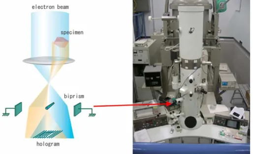
Fig. 1.2 Schematic of the electron holography and the image of a TEM equipped with a biprism.
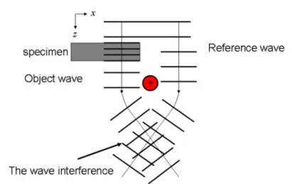
The technique of off-axis electron holography basically depends on the interference of two (or more) coherent electron waves that combine to produce an interferogram or hologram. Off-axis electron holography involves two steps. The amplitude and phase distributions in the image plane of a TEM are first recorded in an electron hologram by interfering reference and object electron beams, and then reconstructed by an optical or digital procedure. To acquire an off-axis electron hologram, the region of interest on the specimen should be positioned to cover half the field of view. An electron hologram is produced by the application of voltage to the biprism with half of the electron wave passing through the vacuum as the reference wave and the other half of the electron wave passing through the specimen as the object wave. The amplitude and the phase distribution of the electron wave from the specimen are recorded in the intensity and the position of the holographic fringes, respectively.
settings to make the incident illumination highly elliptical. The specimen is positioned to cover roughly half the field of view. The electron biprism consists of a conductive filament supplied with a voltage, and two grounded electrode platelets. The conductive filament is usually a thin (<1 mµ ) metallic wire or quartz fiber coated with gold or platinum, which is biased by means of an external power supply or battery [22]. Although the biprism may be located at one of several alternative points along the beam path below the specimen, its usual and most conventional positions is in place of one of the selected-area apertures. The interference-fringe spacing and the width of the fringe overlap region are determined by the biprism voltage and the specimen-lens geometry.
When the biprism is aligned to the y direction, the hologram is formed as a result of the interference between the object wave Φo and the reference wave Φr(Fig. 1.3), which are given by,
+ = Φo x y x y i x y i x λ α π η φ ( , )exp ( , ) 2 ) , ( 0 , (1.1) − = Φr x y i x λ α π 2 exp ) , ( . (1.2)
Here xand y are coordinates in the hologram,
φ
0 is amplitude,η
is phase, λ is the electron wavelength, and the reference wave and object wave are tilted by an angleα
.Thus, the image intensity of a conventional TEM image can be described as the modulus squared of an electron wave function:
( )
x,y (x,y)2 02(x,y) I =Φo =φ .This function only records the amplitude distribution of the specimen.
( )
)) , ( 4 cos( ) , ( 2 ) , ( 1 ) , ( ) , ( , 0 2 0 2 y x x y x y x y x y x y x I o r η λ α π φ φ + + + = Φ + Φ = . (1.3)Fig. 1.3 Interference of the object wave and the reference wave.
Thus, the hologram will consist of a series of cosinusoidal fringes (the last term in the Eq. 1.3) superimposed onto the conventional bright-field image (i.e., the first two terms in the Eq.1.3). Any changes in the positions and/or spacing of the interference fringes will reflect the relative phase shift of the electron wave that has passed through different parts of the specimen. The phase term η(x,y) now is contained in the hologram image and can be separated from this image through a reconstruction procedure.
1.3.2 Hologram reconstruction
To obtain amplitude and phase information, by using the followed formula
∫
+∞ ∞ − − = −Q i q Q x dx q ) exp(2 ( ) ) (π
δ
,( )
))] ( exp( ) ( [ ) 2 ( ))] ( exp( ) ( [ ) 2 ( )] ( [ ) ( ) ( ] [ 0 0 2 0 x i x FT Q q x i x FT Q q x FT q q x I FT η φ δ η φ δ φ δ δ − ⊗ + + ⊗ − + ⊗ + = . (1.4)Equation (1.4) describes a peak at the reciprocal space origin corresponding to the Fourier transform of the reference image, a second peak centered on the origin corresponding to the Fourier transform of a bright-field TEM image of the specimen, a peak centered at q=−2Qcorresponding to the Fourier transform of the desired image wave function, and a peak centered at q=+2Qcorresponding to the Fourier transform of the complex conjugate of the wave function.
The reconstruction of a hologram to obtain amplitude and phase information is illustrated in Fig.1.4. Fig.1.4 (a) shows a hologram of a MgO crystal. To reconstruct the amplitude and the relative phase shift of the electron wave function, the hologram is firstly Fourier transformed, then one of the two sidebands is selected digitally and inversely Fourier transformed, as shown in Fig.1.4 (b)-(d). The amplitude and phase of this complex wave function are then easily calculated.
Fig. 1.4 (a) Off-axis electron hologram recorded from a MgO crystal; (b) Fourier transformation (FT) of the hologram; (c) The selected side band; (d) Reconstructed phase image after inverse Fourier transformation (IFT).
separate the side band with the center band; therefore, the reconstructed image will contain errors originating from the mixing of the diffraction components.
1.3.3 Phase shift by magnetic and electric fields
In general, for electric and magnetic fields given by the electric potential and the magnetic field, respectively, the phase change
η
of an electron wave that has passed through the specimen, relative to the wave that has passed only through vacuum, is given (in one dimension) by the expression [35]:∫
−∫∫
⊥ = B x z dxdz h e dz z x V C x) E ( , ) ( , ) ( η , (1.5) where z is the incident electron beam direction, x is a direction in the plane of the specimen, V is the electronic potential of the specimen, and B⊥ is the component of the magnetic induction perpendicular to both x and z .The interaction constantCE, which depends on the energy of the incident electron beam, is given by the expression
0 0 2 2 E E E E E CE + + = λπ , (1.6)
Where λ is the wavelength of the incident electron and E and E0 are the kinetic and rest mass electron energies, respectively. CEhas values of 7.29×10⁶, 6.53×10⁶, and 5.39×10⁶rad⋅V−1⋅m−1at 200kV, 300kV, and 1MV, respectively.
Mean inner potential (MIP) V0 is related to the composition and density of the specimen, and can be expressed by =
∫
volVatom x y z dxdydz vol
V0 1 ( , , ) , integrated over the object volume vol .
the relative phase change can be simplified to
∫
⊥ − = B x t x dx h e x t x V C x) E ( ) ( ) ( ) ( ) ( 0 η . (1.7) Differentiation of Eq. 1.7 with respect to x leads to an expression for the phase gradient of[
( ) ( )]
( ) ( ) ) ( 0 B x t x h e x t x V dx d C dx x d E − ⊥ = η . (1.8) The Eq. 1.7 and Eq. 1.8 are fundamental to the measurement and quantification of electric and magnetic fields using electron holography for phase imaging.Fig. 1.5 Schematic illustrating of phase shift and phase gradients for electrostatic and magnetic fields [35].
of phase shift and phase gradients for electrostatic and magnetic fields, respectively. For a non-magnetic specimen, rearrangement of equation above yields
dx x dt dx x d C V E ) ( / ) ( 1 0
η
= . (1.9)Thus, for a specimen of known thickness, such as a cleaved wedge, the MIP can be determined from measurement of the potential gradient, even when there are amorphous over-layers covering the specimen surfaces.
1.3.4 Applications of off-axis electron holography
Off-axis electron holography has been widely used in recent years to obtain phase distribution of electrostatic fields and magnetic fields. Several applications of the usage of off-axis electron holography are shown in Fig.1.6.
In Fig. 1.6 (a), off-axis electron holography has been used to measure two-dimensional electrostatic potentials in both unbiased and reverse biased silicon specimens that each contains a single p-n junction [36]. This technique also used to investigate magnetization reversal mechanisms and remanent states in exchange-biased submicron Co84Fe16/Fe54Mn46 patterned elements [37], the relative
Fig.1.6 (a) Semiconductor physics: built-in voltage across a p-n junction; (b)Nanotechnology: Upper panel: remnant magnetic state in exchange-biased CoFe elements; Lower panel: micromagnetic simulation of the same elements; (c)Field Emission: Electrostatic potential from a biased carbon nanotube; (d)Geophysics: Evolved magnetite elements in the titan magnetite system; (e)Biophysics: Chains of magnetite crystals which grow in magnetotactic bacteria and are used for navigation.
1.4 Other Forms of electron holography
A total of about twenty possible modes of electron holography, distinctly different in either their theoretical basis or their experimental requirements, may be available in recently research [25]. Here, we show phase-shifting electron holography briefly, as follows. This technique has an important advantage over conventional off-axis electron holography, and can provide a higher spatial resolution than conventional techniques based on the Fourier transformation.
are acquired by slightly changing the angle of the incident electron beam, and thus in each hologram the interference fringes are displaced (phase-shifted) while the specimen position remains the same. The intensity at a certain point on a hologram will vary sinusoidally with the shift in the interference fringes. The phase and amplitude are then retrieved from the sinusoidal curve fitted to the intensity at each point.
Fig. 1.7 Illustration of the experimental set up for phase-shifting electron holography [41].
] ) , ( 2 cos[ ) , ( 2 ) , ( 1 ) , , ( 0 2 0 2 w k y x x k y x y x n y x I n r o
θ
η
α
φ
φ
+ − + + = Φ + Φ = , (1.10)where nis an integer numbering of the hologram, φ0(x,y)and η(x,y)are the amplitude and phase of the object wave, respectively,
α
is the angle of the electron waves deflected by the electron biprism, wis the width of the interference area andλ π 2 =
k , where λis the wavelength. The phase term kθnw is the initial phase difference between the object wave and the reference wave in the nth hologram. Therefore, the interference fringes are shifted by tilting the incident electron wave.
Fig.1.8 Reconstruction of object wave at a certain point (x, y) [42].
The object wave is reconstructed from a series of holograms. The intensity at a certain point (x, y) on the holograms will vary sinusoidally by shifting interference fringes. Fig. 1.8 illustrates the plot of intensity as a function of the initial phase
w
1.5 Other techniques for phase measurement
1.5.1 Phase measurement using the transport of intensity equation
Gabor proposed the electron holography technique, which is powerful for measuring both the phase and amplitude of the electron wave that passed through a specimen. However, holography cannot be applied to general cases, since there is a requirement for a vacuum region where the reference wave passes through. In 1983, Teague [43] proposed an equation for wave propagation in terms of phase and intensity distributions, and showed that the phase distribution may be determined by measuring only the intensity distributions. This equation is named as Transport of Intensity Equation (TIE). The TIE was recently applied successfully to TEM at medium resolution to observe static potential distributions of biological and non-biological specimens or to measure magnetic fields [44-46].
Fig.1.9 Schematic illustration of transport of intensity due to wave propagation [44].
amplitude of the exit wave is almost constant immediately below the specimen exit surface. However, when a modulated wave propagates through empty space, the amplitude at some places will increase and at other places the amplitude will decrease, according to the phase modulation induced by the specimen.
Mathematically, the TIE for electrons exactly corresponds to the Schrodinger equation for high-energy electrons in free space. Namely, the following TIE
)) ( ) ( ( ) ( 2 xyz xyz I xyz I z xy xyφ λπ ∂ =−∇ • ∇ ∂ , (1.11) is obtained, I andφare the intensity and phase distribution, respectively; x and y are the coordinates in the image plane, z is the vertical direction of the beam illumination. Here,
z I ∂ ∂
is an intensity derivative along the wave propagation direction, and 2 xy ∇ is a two-dimensional Laplacian. For known boundary conditions and in the absence of intensity zeros (in-focus intensity), the TIE can be solved uniquely for the phase.
1.5.2 Phase measurement using Lorentz microscopy
Electron moving through a region of space with an electrostatic field and a magnetic field experiences the Lorentz force. The Lorentz force acts normal to the travel direction of the electron, a deflection will occur. The deflection angle is linked to the presence of electric or magnetic fields.
Lorentz microscopy is all about introducing controlled aberrations in the transfer function of the microscopy in order to induce visible contrast. There are two modes in Lorentz microscopy [47]: the Fresnel mode, in which you observe domain walls and magnetization ripples, and the Foucault mode, where domains are imaged.
domain wall motion under the application of an external magnetic field. It gives essentially qualitative information.
Fig.1.10 Schematic of the electron path through a magnetic specimen in Fresnel mode.
The Foucault mode: this mode corresponds to a bright field image mode in conventional TEM. This means that you select a part of your beam with an aperture located in the back focal plane of your imaging lens. The electrons that pass through the aperture will appear bright whereas the others will appear dark. The deflection angles linked to magnetization are small and you cannot really differentiate them from the transmitted beam, you have to put the aperture quite close to the transmitted beam. Getting nice results in this mode is therefore trickier than getting data from the Fresnel mode.
1.6 Aims and contents in this thesis
In conventional off-axis electron holography based on Fourier transformation method, the spatial resolution of the reconstructed phase image is limited by the fringe spacing. However, the aim of this research is to develop a new method which can overcome the limitation between the spatial resolution and the fringe spacing. Under the use of a stage-scanning system, a stage-scanning electron holography is proposed which has the property to overcome the limitation mentioned above. Based on the stage-scanning electron holography, a technique of super-resolution phase reconstruction is presented for improving the spatial resolution of the reconstructed phase image.
There are five chapters in this thesis, which are organized as follows:
In this first chapter, the outline and history of electron holography, basic knowledge of off-axis electron holography and reconstruction procedure based on Fourier transformation method; other forms of electron holography as well as other method for phase measurement and the aim of this thesis are described.
In the second chapter, a stage-scanning electron holography technique is proposed, which can directly acquire an interferogram, that is, cosine image of phase distribution. The interferogram is constructed by shifting the specimen in one direction with a stage-scanning system and acquiring line intensities of holograms. Under phase object approximation, the object phase can be readily obtained from the interferogram without any reconstruction procedure. The spatial resolution of phase is determined independently of the fringe spacing, overcoming the limitation of conventional techniques based on the Fourier transformation method.
In the third chapter, the stage-scanning electron holography is improved and extended for non-phase object. The resolution improvement is also demonstrated by observing cobalt nanoparticles through comparing the stage-scanning holography and the conventional holography, and significantly sharper images were obtained with the former technique.
stage-scanning electron holography when the scan step of the stage-scanning is a sub-pixel distance. The process of the acquired series of holograms with sub-pixel specimen shift results in a higher pixel density and spatial resolution as compared to the phase image obtained with conventional holography. The final resolution exceeds the limit of the CCD pixel size divided by the magnification.
Reference
[1] D. B. Williams and C. B. Carter (1996) Transmission electron microscopy: A textbook for materials science. Plenum press, New York and London.
[2] E. Ruska (translated by T. Mulvey) (1980) The early development of electron lenses and electron microscopy. Stuttgart, Hirzel.
[3] M. M. Freundlich (1963) Origin of the electron microscope. Science 142: 185-188. [4] E. Ruska (1986) Nobel lecture.
[5] B. Voutou and E. C. Stefanaki (2008) Electron microscopy: The basics. Physics of advanced materials winter school.
[6] A. Delong, K, Hladil, V. Kolarik and P.Pavelka (2000) Low voltage electron microscope 1. Design, 2. Application, 3. Present and future possibilities. EUREM 12. [7] A. M. Glauert (1974) The high voltage electron microscope in biology. J. cell. boil. 63:717-748.
[8]http://en.wikipedia.org/wiki/File:Scheme_TEM_en.svg.
[9] B. Fultz and J. Howe (2007) Transmission electron microscopy and diffractometry of materials. Springer.
[10] P. E. Champness (2001) Electron diffraction in the transmission electron microscope. Garland Science.
[11] A. Hubbard (1995) The handbook of surface imaging and visualization. CRC Press.
[12] R. Egerton (2005) Physical principles of electron microscopy. Springer. [13] E. Kirkland (1998) Advanced computing in electron microscopy. Springer.
[14] R. F. Egerton (1996) Electron energy-loss spectroscopy in the electron microscope. Springer.
[15] J. M. Cowley and A. F. Moodie (1957) The scattering of electrons by atoms and crystals. A new theoretical approach. Acta Crystallographica. 199(3): 609-619.
[16] A. Tonomura (1992) Electron –holographic interference microscopy, Adv. Phys. 41: 59-103.
Adv. Opt. Electron Microsc. 12: 25-91.
[18] D. Gabor (1948) A new microscopic principle, Nature 161: 777-778.
[19] D. Gabor (1949) Microscopy by reconstructed wave-fronts, Proc.R.Soc. A. 197:454-87.
[20] M. E. Haine and T. Mulvey (1952) The formation of diffraction image with electrons in the Gabor diffraction microscope, J.Opt.Soc.Am. 42: 763.
[21] E. H. Leith and J. Upatnieks (1962) Reconstructed wavefronts and communication theory, J.Opt.Soc.Am. 52: 1123-30.
[22] H. Lichte and M. Lehmann (2008) Electron holography-basics and applications, Rep. Prog. Phys. 71:016102.
[23] G. M¨ollenstedt and H. Wahl (1968) Elektronenholographie und Rekonstruktion mit Laserlicht, Naturwissenschaften 55: 340-1.
[24] H. Wahl (1975) Bildebenenholographie mit Elektronen Thesis University of T¨ubingen.
[25] J M Cowley (1992) Twenty forms of electron holography, Ultramicroscopy 41: 335-348.
[26] A. Tonomura, T. Matsuda, J. Endo, H. Todokoro and T. Komoda (1979) Development of field-emission electron microscope, J. Electron Microsc. 28:1-11. [27] T. Fujita, K. Yamamoto, M. R. McCartnet, and D. J. Smith (2006) Reconstruction technique for off-axis electron holography using coarse fringes. Ultramicroscopy 106: 486-491.
[28] Q. Ru, J. Endo, T. Tanji and A. Tonomura (1991). Phase-shifting electron holography by beam tilting. Appl Phys Lett 59: 2372.
[29] G. Lai, Q. Ru, K. Aoyama and A. Tonomura (1994). Electron-wave phase-shifting interferometry in transmission electron microscopy. J Appl Phys 76: 39. [30] W. J. de Ruijter, J.K. Weiss (1993) Detection limits in quantitative off-axis electron holography. Ultramicroscopy 50: 269.
Phase-shifting electron holography for atomic image reconstruction. J. Electron Microsc.59: s81-s88.
[33] K. Harada, A. Tonomura, T. Matsuda, T. Akashi and Y. Togawa (2004). High-resolution observation by double-biprism electron holography. J Appl Phys 96: 6097.
[34] H. Lichte, M. Linck, D. Geiger and M. Lehmann (2010). Aberration correction and electron holography. Microsc Microanal 16:434-440.
[35] M. R. McCartney and D. J. Smith (2007) Electron holography: Phase imaging with nanometer resolution, Annu. Rev. Mater. Res. 37:729-767.
[36] A. C. Twitchett, R. E. Dunin-Borkowski, R. J. Hallifax, R. F. Broom and P. A. Midgley (2003) Off-axis electron holography of electronstatic potentials in unbiased and reverse biased focused ion beam milled semiconductor devices, J. Microscopy 214: 287-296.
[37] R. E. Dunin-Borkowski, M. R. McCartney, B. kardynal, M. R. Scheinfein and D. J. Smith (2001) Off-axis electron holography of exchange-biased CoFe/FeMn patterned nanostructures, J. Appl. Phys. 90:2899.
[38] J. Cumings and A. Zettl (2002) Electron holography of field-emitting carbon nanotubes, Phys. Rev. Lett. 88: 056804.
[39] R. J. Harrison, R. E. Dunin-Borkowski and A. Putnis (2002) Direct imaging of nanoscale interactions in minerals, Proc. Nat. Acad. Sci. 99:16556-16561.
[40] E. T. Simpson, T. Kasama, M. P¨osfai, P. R. Buseck, R. J. Harrison and R. E. Dunin-Borkowski (2005) Magnetic induction mapping of magnetite chains in magnetotactic bacteria at room temperature and close to the Verwey transition using electron holography,J. Phys. Conf. Ser. 17: 108-121.
[41] Q. Ru, G. Lai, K. Aoyama, J. Endo and A. Tonomura (1994) Principle and application of phase-shifting electron holography. Ultramicroscopy. 55: 209-220. [42] K. Yamamoto, T. Hirayama, T. Tanji and M. Hibino (2003) Evaluation of high-precision phase-shifting electron holography by using hologram simulation. Surf. Interface Anal. 35: 60-65.
Opt. Soc. Am 73:1434-1441.
[44] K. Ishizuka and B. Allman (2005) Phase measurement in electron microscopy using the transport of intensity equation, Microscopy Today, 22-24.
[45] M. R. Teague, (1983) Deterministic phase retrieval: a Green’s function solution, J. Opt. Soc. Am. 73:1434-1441.
[46] T. C. Petersen, V. J. Keast, K. Johnson and S. Duvall (2007) TEM-based phase retrieval of p-n junction wafers using the transport of intensity equation, Philosophical Magazine, 87: 3565-3578.
Chapter 2 Development of stage-scanning electron holography
2.1 Introduction
Electron holography is a powerful transmission electron microscopy technique [1-5], which yields quantitative information on the phase and amplitude of electrons passed through a specimen with high spatial resolution, whereas only the intensity distribution can be obtained with conventional electron microscopy. Since the development of the field emission gun and the electron biprism, electron holography has been a popular technique of probing the spatial distribution of electric or magnetic field [6-9]. In electron holography, the amplitude and phase distributions are first recorded in an electron hologram and then reconstructed by an optical or digital reconstruction system. Reconstruction procedures involving Fourier transformation are widely used to extract the phase and amplitude information; in these procedures the electron hologram is Fourier transformed, and then the selected sideband is inversely Fourier transformed. A serious drawback of this procedure [10-14] is that the spatial resolution of the reconstructed electron holography image is limited by the fringe spacing of the hologram. Generally, the fringe spacing should be narrower than one-third of the spatial resolution required in the reconstructed image. Efforts have been made to make fringes narrower to improve the resolution; however, this results in coherence loss.
interferogram. Under a phase object approximation, a phase image can be easily obtained from the interferogram without Fourier transformation.
2.2 Development of stage-scanning electron holography
2.2.1 Principle and experimental methods
Fig.2.1 Schematic of electron holography with a stage-scanning specimen holder.
system enables three-dimensional (3D) scanning of the specimen in a fixed electron optics configuration and has been used for scanning confocal electron microscopy in a conventional transmission electron microscope. Figure 2.2 (a) shows a photograph of the holder head. A tubular piezoelectric actuator is used for moving the stage. Figure 2.2 (b) shows a schematic of the stage-scanning system, which includes the specimen holder, power supply and control program running on a PC.
Fig.2.2 (a) Head of the specially designed TEM specimen holder; (b) schematic of the stage-scanning system comprising the specimen holder, power supply and control unit.
When the biprism is aligned to the y direction, the hologram is formed as a result of the interference between the object wave Φo and the reference waveΦr, which are given by
[
( , )]
exp ) , ( ) , , (n x y 0 x n x y i x n x y o = − ∆ − ∆ Φ φ η , (2.1) = Φr x y i x λ α π 2 exp ) , ( . (2.2)is the scan step width of the specimen movement in the x direction, n is the step number, λ is the electron wavelength, and the reference wave is tilted by an angle
α
relative to the object wave. The hologram intensity is expressed by(
)
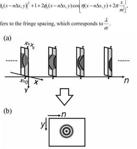
= − ∆ + + − ∆ − ∆ + m x y x n x y x n x y x n x y x n I , , φ0( , )2 1 2φ0( , )cosη( , ) 2π , (2.3)here m refers to the fringe spacing, which corresponds to αλ .
Fig. 2.3 (a) A series of holograms in which only one line intensities at x=0 are captured; (b) the interferogram (cosine image of phase distribution) reconstructed from the line intensities in the holograms.
Assuming that line intensities in each hologram are captured at x=0 in the hologram plane, as schematically shown in Fig. 2.3 (a), the line intensities along the y axis in the hologram with n-th specimen position are expressed by
change is negligible, the amplitude φ0(−n∆x,y) can be replaced by 1 and the phase ) , (−n∆x y η can be calculated as − Π = ∆ − − ( , ) 1 2 1 cos ) , ( n x y 1 n y η . (2.5)
As the line intensities in each hologram along a fixed line x=0 are recorded during the scan, the phase of this line can be obtained from Eq. (2.5) under phase object approximation, and the phase image can be easily reconstructed with a computer. This procedure does not use Fourier transformation, and therefore its spatial resolution is only limited by the scan step width and microscope resolution, not by the fringe spacing.
A JEOL JEM-ARM200F microscope equipped with a biprism was used for testing the proposed technique at an accelerating voltage of 200 kV. The “STEM Diffraction Imaging” software of Gatan Inc. was used to control the holder and acquire holograms.
2.2.2 Results and discussion
obtained in situ using the line CCD intensities at marked positions by lining up the line intensities side by side as the scan goes on. (Although the acquisition speed is still limited by the exposure time.) This example illustrates that the phase can readily be obtained by a single scan of the specimen.
Fig.2.4 (a) TEM image of the MgO crystal; (b) a hologram extracted from the 3D data cube of holograms, an interferogram is obtained by slicing the 3D data cube along the red line; (c) the phase image obtained from the interferogram.
Another example of MgO crystal is presented in Fig. 2.5. In this example, phase changes of about 6 due to the thickness variation can be observed despite a slight π bending of the phase profiles due to the specimen drift. The interferogram (i.e. the phase image) can be obtained in situ using the line CCD intensities at marked positions by lining up the line intensities side by side as the scan goes on.
phase acquisition. Furthermore, this procedure does not use Fourier transformation, and therefore its spatial resolution is only limited by the scan step and microscope resolution, but not by the fringe spacing. An isotropic resolution can be achieved if the scan step is equal to the CCD pixel size divided by the magnification.
Fig. 2.5 (a) TEM image of the MgO crystal with tilted [110] incidence; (b) a hologram extracted from the 3D data cube of holograms, an interferogram is obtained by slicing the 3D data cube along the red line; (c) the phase image obtained from the interferogram.
average the obtained phase images from each line to reduce the exposure time at a given electron beam intensity and signal to noise ratio. In practice, because the resolution does not depend on the fringe spacing, a wider interference fringe which has a higher contrast can be used for reconstruction. Thus, the exposure time can be reduced for achieving the same signal to noise ratio.
2.3 Stage-scanning electron holography with a digital aperture
In the above section, a 3D data cube was recorded and sliced at a fixed position to form an interferogram, which was the cosine image of phase distribution. However, there is another method which also is possible for acquisition of the phase distribution. In this case, a 4D data cube of the holograms is recorded on which the specimen has different positions and then the phase information is separated through a digital aperture from the 4D data cube. Detailed information of this method is as follows.
2.3.1 Methods
Electron waves passing through the specimen and vacuum regions are deflected by the electrostatic potential around the biprism so that an electron hologram is formed on the image plane. With the 2D movement of the specimen in the object plane, 2D holograms can be obtained, resulting in a 4D data array that can be expressed as
+ + ∆ − ∆ − ∆ − ∆ − + + ∆ − ∆ − = y x y x y x y x y x m y m x y n y x n x y n y x n x y n y x n x y x n n I π π η φ φ 2 2 ) , ( cos ) , ( 2 1 ) , ( ) , , , ( 0 2 0 . (2.6)
By applying a pinhole aperture to the origin (x=0, y=0) of holograms recorded at different specimen positions, an interferogram can be obtained as
[
( , )]
cos ) , ( 2 1 ) , ( ) 0 , 0 , , (n n 0 n x n y 2 0 n x n y n x n y I x y =φ − x∆ − y∆ + + φ − x∆ − y∆ η − x∆ − y∆ . (2.7) Under the phase object approximation, the phase distribution can be easily calculated from the interferogram.2.3.2 Results and disctssion
Fig. 2.6 Two extracted holograms of the Co particle (a) and (b), the specimen was moved from the position in hologram (a) to the position in hologram (b) using the scanning stage; (c) The interferogram which corresponds to the phase distribution.
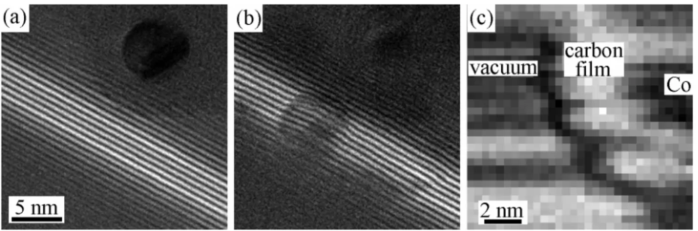
Figures 2.6(a) and (b) show two holograms recorded for two positions of a Co particle with a diameter of 6 nm on an amorphous carbon film. The particle was moved into the fringe area and shifted the fringes as observed in Fig. 2.6(b). The fringe spacing is 0.6 nm in both holograms.
biprism drift during the acquisition.
Fig. 2.7 (a) Electron hologram of the Co particle obtained by conventional electron holography; (b) phase image of the Co particle reconstructed from the hologram (a).
For comparison, the phase of the same particle was obtained by conventional electron holography using the Fourier transformation reconstruction method. Fig. 2.7 (a) shows the hologram recorded by conventional holography of the Co particle. In conventional electron holography, due to the limitation between spatial resolution and fringe spacing, a finer fringe spacing of 0.2 nm was used. A hologram without specimen was taken as a reference. Figure 2.7(b) shows the reconstructed phase image from the hologram of the Co particle.
Fig.2.8 Line profile of the measured phase shift across the Co particle using conventional electron holography.
2.4 Conclusions
Reference
[1] A. Tonomura (1992) Electron –holographic interference microscopy, Adv. Phys. 41: 59-103.
[2] H. Lichte and M. Lehmann (2008) Electron holography-basics and applications, Rep. Prog. Phys. 71:016102.
[3] A. Tonomura (1987) Rev Mod Phys. 59:639-69.
[4] A. Tonomura, T. Matsuda, J. Endo, H. Todokoro and T. Komoda (1979) J Electron Microsc. 28:1-11.
[5] D. Gabor (1949) Proc. R. Soc. London, Ser. A 197: 454.
[6] W. J. de Ruijter (1995) Imaging properties and applications of slow-scan charge-coupled-device cameras suitable for electron microscopy, Micron 26: 247-75. [7] W. J. de Ruijter, J. K. Weiss (1993) Detection limits in quantitative off-axis electron holography, Ultramicroscopy 50:269-83.
[8] D. J. Smith, W. J. de Ruijter, J. K. Weiss and M. R. McCartney (1999) Quantitative electron holography. In introduction to electron holography, ed. E Volkl, LF Allard, DC Joy, pp. 1107-24, New York: Kluwer.
[9] A. Tonomura, T. Matsuda, J. Endo, H. Todokoro and T. Komoda (1979) Development of field-emission electron microscope, J. Electron Microsc 28: 1-11. [10] T. Fujita, K. Yamamoto, M. R. McCartney and D. J. Smith (2006) Reconstruction technique for off-axis electron holography using coarse fringes, Ultramicroscopy 106: 486-491.
[11] K. Yamamoto, T. Hirayama, T. Tanji (2004) Off-axis electron holography without Fresnel fringes, Ultramicroscopy 101: 265-269.
[12] Q. Ru, J. Endo, T. Tanji and A. Tonomura (1991) Phase-shifting electron holography by beam tilting, Appl. Phys. Lett. 59:2372.
[14] Q. Ru, G. Lai, K. Aoyama, J. Endo and A. Tonomura (1994) Principle and application of phase-shifting electron hlography, Ultramicroscopy 55: 209-220. [15] Takeguchi M, Shimojo M, Tanaka M, Che R, Zhang W and Furuya K (2006) Electron holographic study of the effect of contact resistance of connected nanowires on resistivity measurement. Surf Interface Anal. 38: 1628-1631.
[16] M. Takeguchi, K. Mitsuishi, D. Lei and M. Shimojo (2011) Development of sample-scanning electron holography, Microsc Microanal. 17(Suppl 2):1230.
Chapter 3 Improvement of stage-scanning electron holography
3.1 Introduction
3.2 Improvement of stage-scanning electron holography for a non-phase object
3.2.1 Principle
The optical configuration in this improved stage-scanning electron holography is the same with the technique presented above, which has been shown in Fig. 2.1. A collimated electron beam illuminates the specimen which is positioned to cover half the field of view. An interference pattern or a hologram is produced by the application of voltage to the biprism located below the specimen with the reference wave and the object wave. The specimen can be moved by the stage-scanning system [1-3].
When the biprism is aligned to the y direction, the hologram is formed as a result of the interference between the object wave Φo and the reference waveΦr, which are given by
[
( , )]
exp ) , ( ) , , (n x y 0 x n x y i x n x y o = − ∆ − ∆ Φ φ η , (3.1) = Φr x y i x λ α π 2 exp ) , ( . (3.2)Here xandy are coordinates in the hologram, φ0 is amplitude, η is phase, ∆x is the scan step width of the specimen movement in the x direction, n is the step number, λ is the electron wavelength, and the reference wave is tilted by an angle
α
relative to the object wave. The hologram intensity is expressed by(
)
+ ∆ − ∆ − + + ∆ − = m x y x n x y x n x y x n x y x n I , , φ ( , ) 1 2φ0( , )cosη( , ) 2π 2 0 , (3.3)here, m refers to the fringe spacing, which corresponds to αλ .
For a non-phase object in which the amplitude change is not negligible, the simple procedure described in the Eq. (2.5) is not suitable. In this case, the reconstruction procedure for the phase-shifting holography [4, 5] can be applied with a modification.
specimen position remains the same. The intensity at a certain point on a hologram will vary sinusoidally with the shift in the interference fringes. The phase and amplitude are then retrieved from the sinusoidal curve fitted to the intensity at each point.
Fig. 3.1 (a) A series of holograms in which only one line intensities at x=0 are captured; (b) aligning the specimen positions in the acquired holograms; the red dotted frames indicate image positions before the alignment.
proposed below.
In this procedure, aligning the holograms not in the x-y plane but in the n-y plane is performed. A series of 2-dimensional (2D) holograms with different specimen positions can be viewed as a 3D data cube with the dimensions (x, y,∆x⋅n). Slicing this cube in the (y,∆x⋅n) plane at x=xkextracts an interferogram as follows + ∆ − ∆ − + + ∆ − = Π m x y x n x y x n x y x n x y n k k k k k( , ) φ ( , ) 1 2φ0( , )cosη( , ) 2π 2 0 . (3.4)
Fig. 3.2 (a) Images obtained by slicing the 3D data cube at different xk positions; (b)
they are aligned by shifting each slice along the arrows. The red dotted frames indicate image positions before the alignment.
The fringe spacing m was set to be an integer and a multiple of CCD pixel size in this chapter. Thus xk can be expressed as k
N m
the first step is aligning the interferograms in the (y,∆x ⋅n) plane by shifting them in the n-y plane rather than x-y plane, so that the specimen position remains the same in the (y,∆x⋅n) plane. The same specimen points (n,y) on slice x0 and
) , '
(n y on slice xk are related as k x N m n n ∆ + = ' . (3.5) After the slice xk is shifted by k
x N
m
∆ pixels in the direction n, as indicated by the arrows in Fig. 3.2(b), the specimen positions of these two slices overlap when viewed along the direction x. Each new shifted image Π'k(n,y) (the interferogram in red frame) is defined as
+ ∆ − ∆ − + + ∆ − = ∆ + Π = Π N k y x n y x n y x n y k x N m n y n k k π η φ φ ( , ) 1 2 ( , )cos ( , ) 2 ) ), (( ) , ( ' 0 2 0 . (3.6)
Contrary to the phase-shifting technique, since the electron optics is fixed, there is no initial phase term in this expression; instead, the phase difference
N k π
2 appears in the xk slice. Note that since the data cube is sliced at differentxk, the carrier fringe is absent in Eq. (3.6).
After this alignment, the reconstruction procedure is similar to that of phase-shifting holography. Multiplying by
− N k i π 2
exp , and summing both sides
of the Eq. (3.6) over k yields
Then, the phase image and amplitude image can be obtained, respectively, as ) ( tan ) , ( 1 C S y x n∆ = − −
η
, (3.10) 2 2 0 1 ) , ( C S N y x n∆ = + −φ
. (3.11) Consider that in the proposed reconstruction procedure, a total of N1 2Dholograms of N2×N3 size are recorded. Here, N1 is the number of steps; N2 and N3
are the number of pixels within one fringe along the y and x direction, respectively. Retrieval of the phase image requires N1×N2×N3 operations for shifting the interferograms and another N1×N2×N3 operations for calculating the phase. Because the data size in the x direction can be small in our reconstruction procedure, N3 can be much smaller than N1.
The phase-shifting technique requires N1×N2×N3 operations, where N1 is the
number of beam tilts (phase shifts). Let us compare it with the Fourier transformation method for a N2×N3 hologram. The number of calculations is
) (
log )
(N2×N3 2 N2×N3 for Fourier transformation by fast Fourier transform (FFT) and (N2×N3)log2(N2×N3) for the inverse transformation. Thus if N2×N3 is large then the total amount of calculation is much smaller for the Fourier transformation method than for the phase-shifting method or our proposed method. However, the quality of the result in terms of resolution and precision is different, so that direct comparison is difficult.
3.2.2 Experimental methods
Fig.3.3 TEM image of the MgO crystals.
Experiments were carried out by a JEOL JEM-ARM200F microscope equipped with a biprism. MgO crystals were chosen as the specimen to take stage-scanning electron holography. A MgO crystal (Fig.3.3) of about 15 nm in size attached to a large MgO crystal was chosen as a specimen, and a 3D data cube of holograms with the fringe spacing as 1.1 nm was recorded. The scan step width and the total number of scan steps were 0.11 nm and 200, respectively. In this case, the scan step width was equal to the CCD pixel size. The total acquisition time was about 3 min. 30 s including data transfer time and 1 second exposure time for each scan step.
In order to demonstrate that the proposed reconstruction procedure can determine the object wave independently of the fringe spacing, another 3D data cube was recorded with the same MgO crystal but with wider fringe spacing as 2.2 nm.
3.2.3 Results and discussion
in the vacuum region in Fig.3.4 (c) may originate from the charge up of the MgO crystal, but it could also be an artifact which originates from a drift of the biprism, which is difficult to avoid in practice. Thus the line profiles of the net phase shift along the horizontal direction indicated in Figs. 3.4(c) were calculated by subtracting the reference profiles, taken across vacuum regions (lines c2), from the profiles crossing the specimen (lines c1). The resulting profiles are shown in Fig. 3.5. Phase shifts were also measured by a conventional Fourier transformation method with the same fringe spacing of 1.1 nm. The hologram and reconstructed phase image are shown in Fig. 3.6. The profile of phase shift across the MgO crystal indicated in Fig. 3.6 (b) is also added in Fig.3.5 (the red line).
Fig.3.4 (a) and (b) Holograms corresponding to different positions of the MgO crystals; (c) the phase image obtained with the reconstruction procedure for a non-phase object.
Fig.3.5. Line profiles of the measured net phase shift across the MgO crystal using the reconstruction procedure with the fringe spacing m=1.1 nm, and the conventional holography with the fringe spacing m=1.1 nm. The net phase shift was measured along the horizontal (c1) direction indicated in Figs. 3.4(c).
It is claimed that in the proposed technique the spatial resolution is not limited by the fringe spacing. That means holograms with coarse fringes can be reconstructed. As is known, in conventional electron holography, after the hologram is Fourier transformed, its selected sideband is inversely Fourier transformed. To avoid any overlap of the Fourier transformation spectra, the distance between the sideband and the center band
m 1
Fig.3.7 (a) and (b) Holograms corresponding to different positions of the MgO crystals with wider fringe spacing (m=2.2 nm), the reconstruction procedure was applied to the fringe spacing between the two red lines indicated in (a); (c) the phase image obtained from the reconstruction procedure for a non-phase object.
Fig. 3.8 Line profile of the net phase shift calculated by the reconstruction procedure with the fringe spacing m=2.2 nm along the horizontal direction (c1) in Fig.3.7(c).
3.2.4 Drift effect of the biprism and specimen stage and considerations for recording
Several factors should be considered when recording holograms. Since our technique is based on moving the specimen stage to record a series of holograms, special attention should be paid to the drift of the stage perpendicular to the scanning direction. Such drift will hinder alignment of sliced images, resulting in an elongated specimen shape and introducing phase errors. Another experimental factor is biprism drift, which results in intensity shifts and phase shift as mentioned above. This effect can be reduced by stabilizing the prism and by subtracting the background using the vacuum area, provided the electric and magnetic field gradients are neglected.
Fig. 3.9 Fringe drifts during the stage-scanning.
the dotted line in Fig. 3.9 is marked a fixed position on the holograms. When the scan step was 0, the dotted line indicated a bright fringe. When the scan step was 255, the bright fringe shifted to another position on the left side of the dotted line. In this case, the fringe shifted about 46 pixels from the beginning of the stage scan to the end. The fringe spacing was about 20 pixels averaged, that means the phase change corresponds to the fringe drift is about 14.4 radians. This phase change presents as the background phase along the horizontal direction in reconstructed phase image. For example, a reconstructed phase image according to our principle using the series of holograms contained biprism drifts is shown in Fig.3.10. Because analyzing the phase change in the vacuum area will show us the influence of the fringe shift. Fig. 3.10 (a) shows the reconstructed phase image of this vacuum area. The profile along the line indicated in Fig.3.10 (a) shows the background phase across vacuum area, which is about 14.2 radians (Fig.3.10 (b)). This value is almost in accordance with the one calculated by measuring the fringe shifts.
Fig.3.10 (a) shows the reconstructed phase image of a vacuum area; (b) the line profile indicated by the line in (a) shows the background phase across vacuum area.
(
)
+ ∆ + + ∆ + + + ∆ + = n d m x y x n x y x n x y x n x y x n Iη
π
η
φ
φ
( , ) 1 2 ( , )cos ( , ) 2 , , 0 2 0 . (3.12)Slicing the recorded data cube at x yields an interferogram k
) 2 ) , ( cos( ) , ( 2 1 ) , ( ) , ( 0 2 0 d k k k k k n m x y x n x y x n x y x n x y n η π η φ φ − ∆ + + − ∆ − ∆ + + = Π . (3.13)
In order to overlap the specimen positions, a procedure of shifting the specimen position is needed under the relation expressed in Eq. 3.5. The shifted interferogram is expressed by ) ) ( 2 ) , ) ( ( cos( ) , ) ( ( 2 1 ) , ) ( ( ) ), (( ) , ( ' 0 2 0 d k k k k k k k x N m n m x y x k x N m n x y x k x N m n x y x k x N m n x y k x N m n y n
η
π
η
φ
φ
∆ + + + ∆ ∆ + − ∆ ∆ + − + + ∆ ∆ + − = ∆ + Π = Π . (3.14) For convenience, Eq. 3.14 is written in complex form( )
⋅ ⋅ ∆ − − + ⋅ ⋅ ∆ + = Π d d k k x N m i N k i C k x N m i N k i C C y n η π ηπ exp exp 2 exp
2 exp , ' 3 2 1 , (3.15) here, we assume 1 ) , ( 2 0 1= −n∆x y + C φ ;
[
i n x y in d]
y x n C2 =φ0(− ∆ , )exp η(− ∆ , )+ η ;[
i n x y in d]
y x n C3 =φ0(− ∆ , )exp− η(− ∆ , )− η ;Multiplying both sides of equation (3.15) by − N k i π 2 exp , and N k i π 2 exp
⋅ ⋅ ∆ − − × + ⋅ ⋅ ∆ = − Π
∑
∑
∑
− − − d N N d N k k x N m i N k i C k x N m i C N k i y n η π η π exp 2 2 exp exp 2 exp ) , ( ' 1 0 3 1 0 2 1 0 (3.16a)∑
∑
∑
− − − ⋅ ⋅ ∆ − + ⋅ ⋅ ∆ × = Π 1 0 3 1 0 2 1 0 exp exp 2 2 exp 2 exp ) , ( ' N d N d N k k x N m i C k x N m i N k i C N k i y n η η π π (3.16b) Next, we define bi a C'2= + , bi a C'3= − ,and equation (3.16.a) and (3.16.b) can be expressed by
(
a bi) (
B a bi)
C A= + + − , (3.17a)(
a bi) (
E a bi)
F D= + + − , (3.17b) where∑
− − Π = 1 0 2 exp ) , ( ' N k N k i y n A π ;∑
− ⋅ ⋅ ∆ = 1 0 exp N d k x N m i B η ; ⋅ ⋅ ∆ − − × =∑
N− k d x N m i N k i C exp 2π 2 exp η 1 0 ;∑
− Π = 1 0 2 exp ) , ( ' N k N k i y n D π ;∑
− ⋅ ⋅ ∆ × = 1 0 exp 2 2 exp N d k x N m i N k i E π η ;∑
− ⋅ ⋅ ∆ − = 1 0 exp N d k x N m i F η .d
η which can be known by measuring the total phase change caused by fringe drift. A and D can be obtained from the summation of series shifted images. Then we can calculate
(
) (
)
(
CE BF)
C B D F E A a − − − − = 2 , (3.18a)(
) (
)
(
BF CE)
C B D F E A b − + − + = 2 , (3.18b) and retrieval to C'2 and C'3 . Corrected phase and amplitude images are reconstructed by d corr n C C y x n η η − ∆ = − )− ) ' Re( ) ' Im( ( tan ) , ( 2 2 1 , (3.19a) and 3 2 0corr(−n∆x,y)= C' ×C' φ . (3.19b)The term nηdin equation (3.17.a) is a slope ratio, meaning ηcorr(−n∆x,y)lying on the phase slope of nηd due to the fringe drift, which results in the background phase change of vacuum area.
3.3 Demonstration of resolution improvement in stage-scanning electron holography
3.3.1 Experimental methods
the scan step and by the microscope resolution or the pixel size along the y direction. This is the principal difference from the conventional holography. Because the Fourier transformation method is unnecessary to reconstruct the phase, coarse fringes with high contrast can be used, which would also be helpful for improving the precision of the reconstructed phase image.
In the session, an experiment was designed by observation Co nano-particles in a low-magnification mode in which the objective lens of the microscope is switched off. To realize the electron holography configuration the first intermediate lens is also turned off, which limits the choice of magnification. Therefore it may be difficult to have an appropriate combination of magnification and fringe spacing for performing conventional electron holography on specimens with micrometer-scale features. The stage-scanning electron holography technique should solve this problem by overcoming the limitation between the spatial resolution and fringe spacing. This flexibility is especially important for observing magnetic specimens, which must be located in a low-field region to avoid unwanted magnetic saturation.
Experiments were carried out in the low-magnification mode with a JEOL JEM-ARM200F microscope (200 kV) equipped with a biprism and a stage-scanning system. Co nanoparticles with a diameter of 10-20 nm deposited on a carbon film were used as a sample.
Fig. 3.11 TEM image of Co particles.
3.3.2 Results and discussion
Fig. 3.12 Two extracted holograms of the Co particles (a) and (b) with a fringe spacing of 26 nm; The specimen moved from the position in hologram (a) to the position in hologram (b) due to the movement of the specimen stage; (c) The phase image obtained with the stage-scanning technique.
Fig. 3.13 Profile of phase change of the Co particle indicated by the white line in Fig. 3 (c).
and signal-to-noise ratio of the holograms given the limited freedom of magnification in this experiment. Figures 3.14(a) and (b) show the hologram and the phase distribution of the Co particles retrieved via Fourier transformation, respectively. It is difficult to distinguish the phase of each Co particle in this reconstructed phase image. Comparing the results from these two techniques, the stage-scanning holography yields higher resolution with a wider fringe spacing than the conventional holography based on the Fourier transformation method. The former technique is useful when fine fringes cannot be obtained but a high resolution is needed.
Fig. 3.14 Hologram taken with a fine fringe spacing of 17 nm by conventional electron holography (a) and the reconstructed phase image (b). The area within the blue box is the same area that was observed by the stage-scanning holography.
3.4 Conclusions
Reference
[1] Takeguchi M, Shimojo M, Tanaka M, Che R, Zhang W and Furuya K (2006) Electron holographic study of the effect of contact resistance of connected nanowires on resistivity measurement. Surf Interface Anal. 38: 1628-1631.
[2] Takeguchi M, Hashimoto A, Shimojo M, Mitsuishi K and Furuya K (2008) Development of a stage-scanning system for high-resolution confocal STEM. J Electron Microsc. 57: 123-127.
[3] M. Takeguchi, K. Mitsuishi, D. Lei and M. Shimojo (2011) Development of sample-scanning electron holography, Microsc Microanal. 17(Suppl 2):1230.
[4] Q. Ru, J. Endo, T. Tanji and A. Tonomura (1991) Phase-shifting electron holography by beam tilting, Appl Phys Lett. 59: 2372(1991).
[5] Q. Ru, G. Lai, K. Aoyama, J. Endo and A. Tonomura (1994) Principle and application of phase-shifting electron holography. Ultramicroscopy. 55: 209-220. [6] K. Yamamoto, Y. Sugawara, M. R. McCartney and D. J. Smith (2010) Phase-shifting electron holography for atomic image reconstruction. J. Electron Microsc. 59: s81-s88.
[7] H. Lichte, D. Geiger, A. Harscher, E. Heindl, M. Lehmann, D. Malamidis, A. Orchowski and W. Rau (1996) “Artifacts in electron holography”, Ultramicroscopy, 64: 67-77.
[8]W.J.de Ruijter and J. K. Weiss (1993) Detection limits in quantitative off-axis electron holography, Ultramicroscopy, 50: 269-283.
[9] K. Yamamoto, T. Hirayama and T. Tanji (2004) Off-axis electron holography without Fresnel fringes, Ultramicroscopy, 101: 265-269.
[10] H. Lichte (2008) Performance limits of electron holography, Ultramicroscopy, 108(3):256-62.
inline electron holography: Experimental comparison, Ultramicroscopy, 110: 472-482. [13] G. Lai, Q. Ru, K. Aoyama and A. Tonomura (1994) Electron-wave phase-shifting interferometry in transmission electron microscopy. J Appl Phys. 76: 39.
Chapter 4 Super-resolution phase reconstruction technique in
stage-scanning electron holography
4.1 Introduction
Images with high resolution are desired and required in most imaging applications because a high resolution image can offer more details that may be critical in various applications. Since the 1970s, charged-coupled device (CCD) and CMOS image sensors have been widely used to capture digital images. These sensors are suitable for most imaging applications; however, the current resolution level and consumer price will not satisfy the future demand [1].
In optical imaging fields, there are many solutions to increase the spatial resolution. The most direct one is to increase the number of pixel per unit area by sensor manufacturing techniques [1]. However, if the pixel size decreases, the amount of light available also decreases. It therefore generates shot noise that degrades the image quality severely. Another method is increasing the chip size to enhance the spatial resolution. However, this approach is not considered effective because large capacitance makes it difficult to speed up a charge transfer rate. The high cost for high precision optics and image sensors is also an important concern in many commercial applications regarding high resolution imaging. Therefore, a new approach toward increasing spatial resolution is required to overcome these limitations of the sensors and optics manufacturing technology.
![Fig. 1.1 Schematic of optical components in a basic TEM [8].](https://thumb-ap.123doks.com/thumbv2/123deta/10124517.1958487/7.892.168.744.266.789/fig-schematic-optical-components-basic-tem.webp)
![Fig. 1.5 Schematic illustrating of phase shift and phase gradients for electrostatic and magnetic fields [35]](https://thumb-ap.123doks.com/thumbv2/123deta/10124517.1958487/16.892.244.653.383.841/schematic-illustrating-phase-shift-gradients-electrostatic-magnetic-fields.webp)
![Fig. 1.7 Illustration of the experimental set up for phase-shifting electron holography [41]](https://thumb-ap.123doks.com/thumbv2/123deta/10124517.1958487/19.892.337.589.330.686/fig-illustration-experimental-set-phase-shifting-electron-holography.webp)

![Fig. 2.5 (a) TEM image of the MgO crystal with tilted [110] incidence; (b) a hologram extracted from the 3D data cube of holograms, an interferogram is obtained by slicing the 3D data cube along the red line; (c) the phase image obtained fro](https://thumb-ap.123doks.com/thumbv2/123deta/10124517.1958487/36.892.176.720.283.650/crystal-incidence-hologram-extracted-holograms-interferogram-obtained-obtained.webp)