京都大学大学院 工学研究科 三浦清貴
第 28 回無機材料に関する最近の研究成果発表会
CW レーザー
YAG レーザー
(ナノ秒)
フェムト秒レーザー
ピー ク パワ ー (W ) パルスのピーク強度が他の レーザーに比べて4~5桁高い
CW レーザー
YAG レーザー
(ナノ秒)
フェムト秒レーザー
ピー ク パワ ー (W ) パルスのピーク強度が他の レーザーに比べて4~5桁高い
<100 fs
1 mJ, 100 fs の場合、瞬間出力が 10
-3J/10
-13s=10
10W=10 GW 日本の原子力発電所の定格出力 1GW よりも大きい。
・ 光る時間が非常に短い
・・・・ 電子から格子振動へのエネルギー 移動時間や応力緩和時間よりも短い
・ 瞬間的に強い電場を発生する
・・・・ 非線形光吸収が効率よく起こる
・ 広い波長範囲で光の位相がそろっている
・・・・ 波形をデザインできる
時間
集光領域のみの相互作用 → 三次元構造改質
Resonance wavelength (e.g., UV laser or light)
The surface
Nonresonance wavelength (femtosecond laser)
The interior
(multi-photon process) high peak power
Nonresonance wavelength (e.g., CW, nanosecond laser
or visible light)
Non-reaction (one-photon process) Glass
Reaction area Non-reaction Reaction area
Optics Letters, Vol.21, No.21, (1996) 1729-1731. 被引用回数:794
Applied Physics Letters, 71, (1997) 3329-3331. 被引用回数:469
fsレーザー材料内部プロセッシングの特徴
その特徴を利用したガラス材料内部構造改質 ガラス材料以外への適用
空間位相変調器(LCOS-SLM)による
ホログラフィック三次元描画
キャリア励起
熱化
キャリア除去
熱伝搬&
構造変化
フォトンの吸収
衝撃イオン化 キャリア-キャリア散乱
キャリア-フォノン散乱 オージェ再結合
放射再結合 キャリア拡散
アブレーション 熱拡散
再固化
10-16 10-15 10-14 10-13 10-12 10-11 10-10 10-9 10-8 10-7 10-6 10-5
fs ps ns µs
10-4 10-3 ms
200 kHz 1 kHz
パルス幅
(フェムト秒オーダー)
パルスの繰り返し周波数
(ナノ秒からミリ秒)
80 MHz
時間
観測条件 波長
パルス幅
対物レンズ
: 800 nm (Probe 光は Pump 光の SHG) : 100 fs
: 50 × (NA=0.80)
BBO Polarizer
Sample
Pump
Probe
Femtosecond laser
Delay line Blue filter
Polarizer CCD camera
時間分解応力波観測システム
8
6
4
2
0
Df (r) phase change
14 12
10 8
6 4
2 0
r/ m m
5000 ps 2000 ps 1600 ps
1000 ps 1200 ps 1400 ps
800 ps
1 ps 100 ps 200 ps 400 ps 600 ps
300 ps
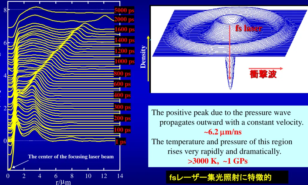
The positive peak due to the pressure wave propagates outward with a constant velocity.
~6.2 mm/ns
The temperature and pressure of this region rises very rapidly and dramatically.
>3000 K, ~1 GPs
Fig. The phase distribution obtained by a phase retrieval calculation of the spatial pattern.
The center of the focusing laser beam
Density
fs laser
衝撃波
fsレーザー集光照射に特徴的
ナノ秒~マイクロ秒
-100ns 0ns 10ns 50ns
100ns 150ns 200ns
50ms 20ms
10ms 4ms
2ms 1.5ms
1ms
300ns
500ns
-100ns 0ns 10ns 50ns
100ns 150ns 200ns
50ms 20ms
10ms 4ms
2ms 1.5ms
1ms
300ns
500ns
-100ns 0ns 10ns 50ns
100ns 150ns 200ns
20ms 50ms 10ms
4ms
2ms 1.5ms
1ms
300ns
500ns
-100ns 0ns 10ns 50ns
100ns 150ns 200ns
20ms 50ms 10ms
4ms
2ms 1.5ms
1ms
300ns
500ns
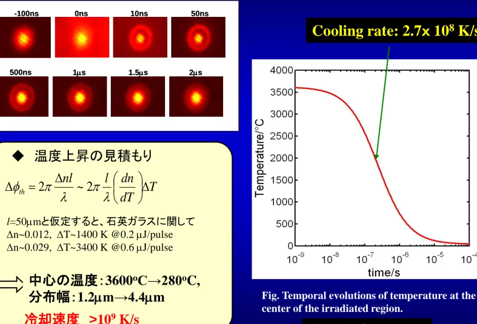
◆ 温度上昇の見積もり dT T
dn l nl
th
D
D
D
f 2 ~ 2
l=50mmと仮定すると、石英ガラスに関して
Dn~0.012, DT~1400 K @0.2 mJ/pulse Dn~0.029, DT~3400 K @0.6 mJ/pulse
中心の温度: 3600
oC→280
oC, 分布幅:1.2mm→4.4mm
冷却速度 >10
9K/s
Cooling rate: 2.7 x 10
8K/s
Fig. Temporal evolutions of temperature at the center of the irradiated region.
熱緩和時間: 10 ms
UV レーザーやナノ秒パルスレーザーとは異なる
• パルスエネルギー 小 → 欠陥生成
• パルスエネルギー 大 → 空洞化
• 繰り返し >100 kHz → 局所溶融,組成移動
The irradiation of a single pulse
Temperature increase and thermo-elastic stress should be induced in a very limited
volume.
↓
The relaxation of the thermo-elastic stress produces the force driving the shock wave.
↓
The shock wave propagates outward.
↓
The structure of the glass is extended outside.
After pulse irradiation Compressive stress moves back
toward the center.
↓
A graduated high-density region is formed in the laser-focusing area.
↓
Structural change becomes a
permanent refractive-index change.
Energy density
Low High
BaO-Al2O3-B2O3glass Laser Beam
Melting region BaO-Al2O3-B2O3glass
Laser Beam
Melting region
1 sec.
30 min.
1 sec.
1 sec.
30 min.
30 min.
β-BBO crystal
20 40 60 80 100
走査距離(mm)
X線強度(任意)
Ba
Al
40 min
Intensity (a.u.)Intensity (a.u.)
Scanning distance (mm) Scanning distance (mm) Ba
Ba Al
Al
0 20 40 60 80 100
走査距離(mm)
X線強度(任意) Ba
Al
0 20 40 60 80 100
走査距離(mm)
X線強度(任意) Ba
Al
1 ps
0 20 40 60 80 100
走査距離(mm)
X線強度(任意)
Ba
Al
40 min
Intensity (a.u.)Intensity (a.u.)
Scanning distance (mm) Scanning distance (mm) Ba
Ba Al
Al
1 sec.
30 min.
非線形光学結晶析出
100μm
Refractive Index
Radial Distance (mm)
-10 -5 0 5 10
1.455 1.460 1.465 1.470 1.475 1.480 1.485
Refractive Index
Radial Distance (mm)
-10 -5 0 5 10
1.455 1.460 1.465 1.470 1.475 1.480 1.485
Objective power (NA) (mW)
Ⅰ 0.25 425
Ⅱ 0.13 425
Ⅲ 0.13 350
Refractive Index
Radial Distance (mm)
-10 -5 0 5 10
1.455 1.460 1.465 1.470 1.475 1.480 1.485
Refractive Index
Radial Distance (mm)
-10 -5 0 5 10
1.455 1.460 1.465 1.470 1.475 1.480 1.485
Objective power (NA) (mW)
Ⅰ 0.25 425
Ⅱ 0.13 425
Ⅲ 0.13 350
高密度化による屈折率変化
TEM
100 nm
TEM
100 nm Au nanoparticle
金属微粒子析出
Photo-reduction Sm3+→Sm2+
Photo-reduction Sm3+→Sm2+
500 550 600 650 700 750 800
Emission intensity (a.u.)
Wavelength (nm)
5 D0→7 F0
5 D0→7 F2
Sm2+
Sm3+
5 D0→7 F1
: 4G5/2-6HJ
: 4G5/2-6HJ J=5/27/2
9/2 Irradiated area Irradiated area
500 550 600 650 700 750 800
500 550 600 650 700 750 800
Emission intensity (a.u.)
Wavelength (nm)
5 D0→7 F0
5 D0→7 F2
Sm2+
Sm3+
5 D0→7 F1
: 4G5/2-6HJ
: 4G5/2-6HJ
: 4G5/2-6HJ
: 4G5/2-6HJ J=5/27/2
9/2 Irradiated area Irradiated area
価数変化
Refractive index reference[%]
Change
diameter[mm] [email protected]
mm Calculated guide
[email protected] Calculated guide [email protected]
I 1.32 20 6.0 6.7
LP01, LP02, LP11 LP01, LP11II 0.53 18 9.0 10.3
LP01, LP11 LP01, LP11III 0.27 11 12.0 13.5
LP01 LP01Table Guide mode and mode field diameter calculated from the refractive-index profile
The characteristics of a writing waveguide can be controlled by adjusting the writing conditions
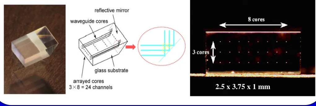
2.5 x 3.75 x 1 mm
250mm
Dammann grating (microscopic view) Photograph of the image pattern
=633nm
Diffraction efficiency = 7.7%
Material : Synthesized silica Laser power : 300mW
Objective lens : 20x (NA0.4)
Scanning speed : 60mm/sec
Binary lens (microscopic view) Image at the focal plane
f=1024mm
z
0
9.0 CCD
=633nm
Material : Synthesized silica Laser power : 160mW
Objective lens : 5x (NA0.14) Scanning speed : 25mm/sec
f=9mm NA=0.057
=633nm
Diffraction efficiency = 38.7%
Spot size = 12.3mm X profile
Y profile
20μ m
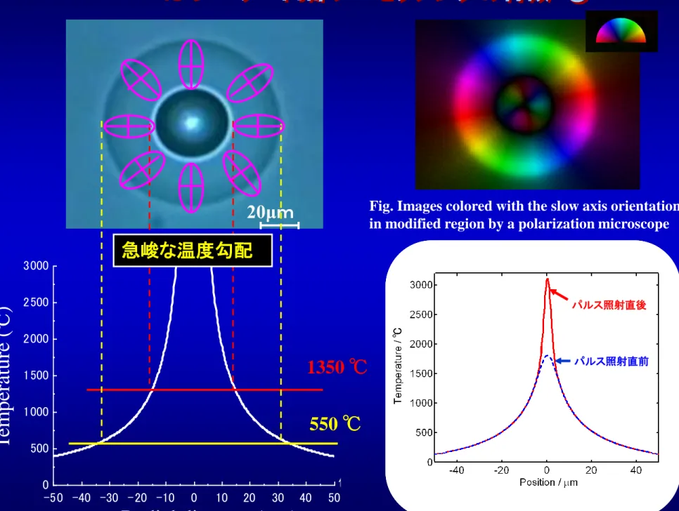
-50 -40 -30 -20 -10 0 10 20 30 40 50 0
500 1000 1500 2000 2500 3000
温度 [℃]
位置 [mm]
Radial distance (mm)
T em per at ur e (
℃)
1350 ℃
550 ℃
Fig. Images colored with the slow axis orientation in modified region by a polarization microscope
急峻な温度勾配
パルス照射直前 パルス照射直後
パルス照射直前 パルス照射直後
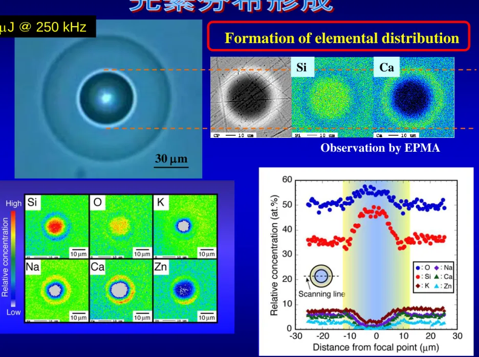
Fig. Elemental distribution around the focal point after laser irradiation and relative concenntration profile of each element across the modified area.
Formation of elemental distribution
Observation by EPMA
Si Ca
30 mm
3.0 mJ @ 250 kHz
P
2O
5-In
2O
3-CaO ガラス
CP
InCa
P
2O
5-Ga
2O
3-CaO ガラス
CP
GaCa
P
2O
5-Al
2O
3-CaO ガラス
CP
AlCa
30 mm 30 mm
P
2O
5-GeO
2-Ga
2O
3-K
2O ガラス
O
Ge Ga
Ca P
CP
O
Ge Ga
K P
CP
Ga
Ge
GaGe
反射電子像
Ga
Ge
GaGe
反射電子像
0 20 40 60 80 100 120
1.52 1.54 1.56 1.58 1.60 1.62 1.64 1.66 1.68
Refractive index
Position (mm)
0 20 40 60 80 100 120
1.52 1.54 1.56 1.58 1.60 1.62 1.64 1.66 1.68
Refractive index
Position (mm)
0 20 40 60 80 100 120
1.52 1.54 1.56 1.58 1.60 1.62 1.64 1.66 1.68
Refractive index
Position (mm)
屈折率差: 0.05 (密度変化では 10
-2オーダー)
10μm 100nm
10μm 100nm
Backscattering electron images on Si rich region in previous slide by field emission scanning electron microscopy.
5nm
10 nm
Silicon nano-particles were precipitated near the focal spot by the fs laser irradiation.
金属 Al 添加シリケート ガラス
5 μ m
(a) (c)
1 μ m
(b)
OO
CaCa AlAl SiSi
Si Si
O O
CaCa AlAl
SiSi
(a) (b) (c)
5 μ m
(a) (c)
1 μ m
(b)
OO
CaCa AlAl SiSi
Si Si
O O
CaCa AlAl
SiSi
(a) (b) (c)
O
O CaCa
Al Al SiSi O
O CaCa
Al
Al SiSi OO
CaCa Al
Al
SiSi
O O
CaCa Al
Al
SiSi
(a) (b)
SEM image and the graph plots the results of elemental analysis by EDS of polished glass surface to depth of focal point.
(a) non-irradiated, (b) laser irradiation and after subsequent heat treatment at 850 ℃.
LASER
Pulse width: 130 fs Pulse energy: 3 mJ
Repetition rate: 200kHz Objective: 50x, NA=0.85 Irradiation Time: 5 sec.
+ Heat treatment at 850 ℃
O Si
Ca Al
Si はガラスの2倍以上の屈折率を有する
1μm↓
Siフォトニクスへの展開
アルカリシリケートガラス
BEI Ca
Si O
10 mm 10 mm
BEI Ca
Si O
BEI Ca
10 mm
Si O
高繰り返し(250 kHz) 低繰り返し(1 kHz)
フェムト秒レーザーの焦点位置:
20 mm
温度分布シミュレーション
1300 C
0 ms 10 ms 50 ms 100 ms 990 ms
Pol ish E
Focusing of single fs-laser beam
SEI BEI
laser E
E
1 µm
laser1 µm
~200 nm
~30 nm
200 nm E
laser
BEI
10 mm
Electron plasma wave propagation
Polarization
Laser light Hot plasma
Plasma wave
Formation of periodic nanostructure
E
k
wk
d
k
wMomentum conservation
d w
pl
k k
k
2 k
d :
周期間隔k
pl プラズマ電子波の 波動ベクトルレーザー光 波動ベクトル
2 0
2 2
pl
3
pl e
e B e
e
k
m κ T ε m
e ω n
2 2
0 2 2
pl 2
w
3
d w
e e B e
e
k k
m κ T ε m
e ω n
ω
プラズマ電子波の分散
Te: 電子温度、ne: 電子密度、me:電子質量、kB:ボルツマン定数、e: 電荷
(001) (101) (111)
応力波シミュレーション
fs-laser condition
rep. rate: 50 Hz ~ 1 kHz pulse duration: 225 fs wavelength: 780 nm pulse energy: ~300 mJ
cell
Objective
20x (NA 0.40)
stirrer
Cu particle
in ethanol solution
Initial
5 mm
5min
5 mm
20 min
200 nm
Cu2O
metal Cu
~ 5 nm
10 nm
500 nm
Linear polarization Circular polarization
500 nm
初期に形成した核がレーザーの偏光方向の影響を受ける 入射光と金属表面のプラズモンとの相互作用
20 nm 20 nm
x y x z
y z
E E
Nd
2Fe
14B
10 nm 固液混合系でのレーザーアブレーション
大気中では;
•生成粒子の回収が困難
•酸化してしまう
単磁区臨界径以下(平均粒径:40 nm)
Field (Oe)
Moment (emu)
Field (Oe)
Moment (emu)
レーザー60 min照射後
Hc : 757 Oe Mr/Ms : 0.4
Field (Oe)
Moment (emu)
レーザー照射前
Hc: 416 Oe Mr/Ms: 0.2
保磁力が約1.6倍増加
Moment (emu)
Field (Oe)
Field (Oe)
Moment (emu)
Field (Oe)
Moment (emu)
レーザー60 min照射後
Hc : 757 Oe Mr/Ms : 0.4
Field (Oe)
Moment (emu)
レーザー照射前
Hc: 416 Oe Mr/Ms: 0.2
保磁力が約1.6倍増加
Moment (emu)
Field (Oe)
Nd
2Fe
14B ナノ微粒子
所望の 電場振幅分布
ランダムな 位相分布
初期値
IFT
振幅を置換 Phase Amp
FT
振幅を置換
Amp Phase
IFT
SLM の直後 加工面
所望の光振幅分布
適当な位相分布 )
, (X Y Fimage
) ,
0
( X Y D
)]
, ( exp[
) ,
( ( )
)
( x y i x y
gobjectm Df m
)]
, ( exp[
) ,
(x y i ( ) x y
fobject Df m Gimage(m) (X,Y) exp[iD(m)(X,Y)]
)]
, ( exp[
) ,
( X Y i
( )X Y
F
image D
m①
②
振幅部分を置換 振幅部分を置換
②
初期値