Doctoral Thesis
Studies on Design Methods for
Topological Quantum Circuits
September 2017
Doctoral Program in Advanced Information Science and Engineering
Graduate School of Information Science and Engineering
Ritsumeikan University
Doctoral Thesis Reviewed
by Ritsumeikan University
Studies on Design Methods for
Topological Quantum Circuits
(トポロジカル量子回路の
設計手法に関する研究
)
September 2017
2017 年 9 月
Doctoral Program in Advanced Information Science and Engineering
Graduate School of Information Science and Engineering
Ritsumeikan University
立命館大学大学院 情報理工学研究科
情報理工学専攻 博士課程後期課程
NURUL AIN BINTI ADNAN
ヌルルアインビンティアドゥナン
Supervisor: Professor YAMASHITA Shigeru
Abstract
A quantum computer is expected to outperform a conventional computer by utilizing some known quantum algorithms; these quantum algorithms are designed to solve important problems such as database search and factorization. However, in practice, to realize a quan-tum computer is still a big challenge for researchers due to occurrence of many errors such as decoherence, etc. Nowadays, topological quantum computation is considered as one of the most promising computation models to realize quantum computation. Therefore, vari-ous studies have been carried out to support the topological quantum computation model. By using topological quantum computation framework, even if a device with a large error is used in operations, a quantum circuit based on the topological quantum computation frame-work is configured in such a manner that errors can be detected and corrected. Thus, by reducing the possibility of errors that can be detected, and correcting them if they happen to occur, a realization of fault-tolerant quantum computation becomes possible. Therefore, we can expect that a quantum computer can be realized by the topological quantum
computa-tion framework. The circuit for topological quantum computacomputa-tion is significantly different
from the conventional circuit even in the logic level; in topological quantum computation, the logical primitive is called a braiding operation. Accordingly, the design strategy for
design.
Considering the above-mentioned expectation of topological quantum computation frame-work, the goal of this thesis is to investigate new optimization methods for designing a quantum circuit that is compatible for the topological quantum computation. This thesis starts with Chapter 1 that gives a brief summary of research interests in topological quan-tum computation and the urge of finding a reliable design method to support the circuit model for topological quantum computation. Then, Chapter 2 explains basic concepts of topological quantum computation necessary for this thesis.
Chapter 3 proposes an efficient design method needed for the topological quantum
com-putation. The proposed design method can adapt with high level description of circuits and design framework starts from the quantum algorithm level and ends at the physical hard-ware level. Furthermore, this thesis also introduces an alternative approach to support the topological quantum computation design flow called ICM representation, which consists of qubit (I)nitialization, (C)ontrolled-NOT gates and (M)easurements with respect to dif-ferent bases. The purpose of ICM is to create a deterministic circuit from probabilistic components (e.g., measurements) and the constructed quantum operations from this form of circuit representation are relatively robust. Thus, this thesis highly recommends the use of the ICM representation. Besides that, this thesis also includes a case study for a practical ICM circuit in order to evaluate the importance of qubit layouts that will be discussed later in more details in Chapter 5.
When designing conventional quantum circuits, the so-called quantum cost is often used to evaluate the quality of circuits. Therefore, Chapter 4 proposes a new method to reduce the quantum cost at the conventional quantum circuit model. The proposed idea
functionality of the given function temporally, so that the modified function has a smaller quantum cost. Then, to compensate for the temporary change, additional gates are inserted into the circuit. In order to apply the idea for a large scale circuits, the proposed method finds a small Exclusive Sums-Of-Products (ESOP) expressions, and then finds a good pair of product terms in the ESOP expression so that the quantum cost can be reduced by ap-plying transformation. The proposed method is expected to achieve better quantum cost reduction than the existing methods, and indeed the experimental results confirmed this expectation.
An interesting feature of topological quantum computation is that by utilizing the prop-erty of braiding operations, it is possible to reduce the computational time steps. Thus, there has been a research to find a good qubit order in one-dimension to satisfy such a property for topological quantum computation. On the other hand, Chapter 5 describes a new method by using two-dimensional qubit layouts for topological quantum computation in order to reduce the computational time steps instead of one-dimensional qubit layouts. The computational time steps of a circuit is expected to be reduced drastically compared to the existing method by arranging qubits in two dimensions by using the proposed method, and indeed the experimental results confirmed this expectation.
Finally, Chapter 6 concludes the investigation of this research and provides possible future work.
Contents
Abstract i
1 Introduction 1
1.1 Problem statement and motivation . . . 3
1.2 Outline of the thesis . . . 5
2 Preliminaries 7 2.1 Basic concepts of quantum circuit model . . . 8
2.1.1 Quantum bits . . . 8
2.1.2 Quantum gates . . . 8
2.1.3 Quantum cost . . . 10
2.2 Basic concepts of topological quantum circuit . . . 11
2.2.1 The defects . . . 11
2.2.2 The braiding operation . . . 12
2.2.3 Surface code . . . 12
2.2.4 Logic circuit model for topological quantum computation . . . 13
3 Design Methods for Topological Quantum Circuits 17
3.1 Design framework for topological quantum computation . . . 18
3.1.1 Quantum algorithm level . . . 19
3.1.2 Quantum circuit level . . . 20
3.1.3 Logical layer (geometric description) level . . . 22
3.1.4 Quantum physical hardware level . . . 23
3.2 An approach to support topological quantum computation design flow . . . 25
3.3 Design flow for topological quantum computation . . . 29
3.4 Conclusion . . . 30
4 Reducing Quantum Cost for Topological Quantum Circuits 32 4.1 Realizing Boolean function with MPMCT gates . . . 33
4.2 Initial circuit generation by minimizing ESOP expressions . . . 37
4.3 A pre-optimization technique to reduce quantum costs . . . 41
4.3.1 General idea and a motivational example . . . 41
4.3.2 How to insert MPMCT gates for a good pre-optimization . . . 44
4.4 Proposed heuristic method . . . 45
4.5 Experimental results . . . 57
4.6 Conclusion and future work . . . 60
5 Reducing Computational Steps for Topological Quantum Circuits 62 5.1 The importance of qubit order for topological quantum circuit model . . . . 63
5.2 A qubit layout optimization problem for topological quantum computation . 66 5.2.1 Terminology used for one-dimensional qubit layout . . . 66
5.2.3 A method to find a good qubit layout . . . 70
5.3 Experimental results . . . 75
5.3.1 An SA-based heuristic method . . . 75
5.3.2 Comparison between one- and two-dimensional qubit layouts . . . 76
5.3.3 Case study: qubit layout problem for a practical ICM circuit. . . 79
5.4 Conclusion . . . 81
6 Concluding Remarks 84
List of Figures
2.1 A NOT gate. . . 9
2.2 A CNOT gate. . . 9
2.3 MPMCT gates. . . 10
2.4 An illustration of a braiding operation for a CNOT gate. . . 12
2.5 Logical qubits with braiding operations. . . 13
2.6 Braiding for a CNOT gate. . . 14
2.7 Overlapped braiding operations. . . 15
2.8 Non-overlapped braiding operations. . . 16
3.1 An example of a quantum circuit. . . 21
3.2 An example of a geometrical representation converted from a quantum circuit. 24 3.3 3-Dimensional lattice of qubits. . . 25
3.4 ICM representation of a controlled-V gate. . . 29
3.5 Design flow for topological quantum computation. . . 31
4.1 Reversible circuit model. . . 34
4.2 The quantum circuit for Table 4.1. . . 36
4.4 Group patterns for Kmap for Table 4.1. . . 40
4.5 The quantum circuit for Fig. 4.4. . . 40
4.6 A bad case for Arabzadeh method. . . 40
4.7 The quantum circuit for Fig. 4.6. . . 40
4.8 Insertion of a CNOT gate before G0. . . 42
4.9 The Kmap after the insertion of the first CNOT gate. . . 42
4.10 The Kmap before the insertion of the first gate. . . 42
4.11 The movement of cells by the insertion of the first CNOT gate. . . 42
4.12 The insertion of the second CNOT gate. . . 43
4.13 The Kmap after the insertion of the two CNOT gates. . . 43
4.14 The insertion of two CNOT gates to restore the original function. . . 44
4.15 The final quantum circuit by the proposed method: Cost 9. . . 44
4.16 Various grouping of adjacent cells for a product term with two literals. . . . 46
4.17 An example of moving 1-value cells. . . 46
4.18 Two MPMCT gates. . . 47
4.19 After applying Merge Rule 1. . . 47
4.20 Two MPMCT gates. . . 48
4.21 After applying Merge Rule 2. . . 48
4.22 An example of a reversible circuit. . . 52
4.23 Inserting a CNOT gate. . . 52
4.24 Type A gates (shaded). . . 53
4.25 Modified Type A gates after an MPMCT gate is inserted. . . 54
4.26 Type B gates (shaded). . . 54
4.28 Type C gate is put after the second CNOT gate to restore the original function. 55
4.29 A Pair of gates that satisfy Merge Rule 1. . . 56
4.30 After merging g5 and g8. . . 56
4.31 Inserting the second pair of CNOT gates. . . 57
4.32 After merging g2 and g4. . . 58
5.1 An initial circuit: 8 Steps. . . 65
5.2 Optimal one-dimensional qubit layout: 3 Steps. . . 65
5.3 Optimal two-dimensional qubit layout: 2 Steps. . . 65
5.4 Graph at Step 1 for circuit in Fig. 5.1. . . 72
5.5 Example of two-dimensional layouts. . . 72
5.6 The original order of CNOT gates in Fig. 3.4. . . 80
5.7 With an optimized qubit layout. . . 82
List of Tables
2.1 Quantum cost of MPMCT gates with m control bits (0 ≤ m ≤ 15). . . 11
4.1 A truth table for a 4-input Boolean function with 4 minterms. . . 35
4.2 Preliminary experimental results. . . 59
4.3 Heuristic experimental results. . . 60
5.1 Comparison of three methods. . . 77
Chapter 1
Introduction
An integrated circuit was first invented in 1958 [1]. Since it was first invented, the perfor-mance of the integrated circuit has continued to improve remarkably for many years, and number of transistors per square inch on the integrated circuit had doubled every year. The development of the integrated circuit has increased exponentially thanks to the Moore’s law, and accordingly the size of transistors has been made smaller and smaller, approach-ing a size of one atom [2]. However, since the size of the transistors has been made smaller approaching a size of one atom, it is impractical to shrink the transistors much more. Thus, it can be predicted that the Moore’s law will no longer be valid in the near future. In other words, we will soon reach a physical limitation in the advancement of cur-rent integrated circuit technology. Therefore, in order to overcome the end of Moore’s law, in recent years a new computation model called quantum computation, which is based on
a completely different calculation method of a current information processing system has
drawn many researchers attention for its implementation and advantages [3], [4], [5]. The quantum computation model uses the advantage of quantum physics (i.e., superposition)
for its operation, and by using this advantage the quantum computer model can offer many promising results, including solving more quickly such important problems as database search and factorization.
Therefore, there is a growing interest in the research community regarding quantum computation model, and various studies have been carried out to realize a quantum com-puter; a computer that performs quantum computation in its operation. However, in prac-tice, to build a fully scalable and reliable quantum computer remains as an extraordinary
challenge for researchers. The realization of the quantum computer seems difficult because
quantum state is susceptible to noise due to external influences such as decoherence, and
thus many errors occur; we need an efficient quantum error correction scheme [6]. In
or-der to solve problems such as error from occurring and to realize a quantum computer, a realization of fault-tolerant quantum computation is regarded as one of the most important tasks. This is because a fault-tolerant quantum computation is capable to perform cal-culation, and at the same time performing error correction if there are some errors exist. Nevertheless, the implementation of fault-tolerant quantum computation is also considered
as challenging. The reason is, when considering practical computing devices it is difficult
to find quantum gates that can perform operation correctly and less susceptible of making errors. Therefore, it is crucial to develop a quantum computer from a model of computation that is build of fault-tolerant quantum gates. Among existing fault-tolerant computational design models, Topological Quantum Computation has attracted much attention due to its unique properties that are essential for error-free computation.
A quantum circuit constructed from this model of computation is in a form that not only can detect errors, but can also simultaneously correcting them if they happen to oc-cur. Thus, by reducing the probability occurrence of errors that cannot be detected, and
simultaneously correcting them if they do exist, the realization of fault-tolerant quantum
computationbecomes possible. Moreover, the topological quantum circuit is also differs
from the conventional quantum circuit model even in the logic level; the logical primitive in topological circuit is called a braiding operation. Therefore, we can expect that a quantum computer can be realized by using topological quantum computational model.
1.1
Problem statement and motivation
Topological quantum computation is considered as one of the most promising computation models to realize quantum computation. The way of encoding logical qubits in topological
quantum circuit is greatly different from the conventional quantum circuit, and thus the
logical primitive operation is also very different. The logical primitive called braiding can
be seen as a drawing line between logical qubits with some special rules when designing a quantum circuit. Therefore, since the properties of the topological quantum circuit are
different from the conventional quantum circuit, the design strategy should also be different
from the conventional quantum circuit design [7].
One of the biggest issues when designing circuit for quantum computation model is one often think on how to evaluate the quality of the quantum circuit. In the conventional quantum circuit, the so-called quantum cost is often used to evaluate the quality of circuits. Therefore, finding ways to design quantum circuits with a lower quantum cost has been considered as one of the major objectives for the researchers for quite a long time. To date, several approaches have been proposed in order to design a quantum circuit that is low in quantum cost for quantum computation model. Accordingly, we may concern about how to reduce the quantum cost when designing circuit for topological quantum computation
model.
In addition, how to build a scalable quantum circuit also remain as one of the ongo-ing issues among the researchers. This is because even though a quantum computer is expected to outperform a conventional computer due to use of quantum properties such as superposition and entanglement, in practice, a quantum computer(quantum operation) is not perfect due to the occurrence of errors such as decoherence, etc. Due to the interference of decoherence, many information lost quickly during the operations. Therefore, one of the important keys to note when designing topological quantum computation is, it is crucial
to minimize the total space or time/volume in topological circuit. This is because space
and volume in topological circuit relate directly to the number of physical qubits and the required computational time to implement the circuit.
Considering the above-mentioned issues, in order to demonstrate the ability of
topo-logical quantum computation, there is a need of an efficient design framework to support
this model of computation. Therefore, this thesis introduces a design flow for topological quantum circuits consisting of four steps: after designing a circuit with the same model as the conventional quantum circuits, the circuit is converted to a topological quantum computation circuit model. Then, this thesis introduces the following contributions of opti-mization methods at the two steps of the design flow. Experimental results confirmed their effectiveness.
The first contribution of this thesis is to propose a new method to reduce the quantum cost at the conventional quantum circuit model. So far, in most of existing design methods, template matching is often used to minimize the gate count in order to find any reduction in quantum cost. In contrast to this, the proposed idea in this thesis involves adding some
gates to change the functionality of the given function temporally so that the modified func-tion has a smaller quantum cost. To compensate for the temporary change, addifunc-tional gates are inserted to the circuit. Furthermore, based on the idea, this thesis proposes a heuris-tic method to reduce the quantum cost for pracheuris-tical (i.e., large) circuits. The proposed method finds a small Exclusive-Sum-Of-Products (ESOP) expression for the function, and then finds a good pair of product terms in the ESOP expression so that the quantum cost can be reduced by applying the transformation to the pair. The proposed method is ex-pected to achieve better quantum cost reduction than the existing methods, and indeed the experimental results confirmed this expectation.
The second contribution of this thesis is to propose a method to reduce the number of computational time steps by utilizing the property of braiding operations in a topological quantum circuit. In the conventional topological quantum circuit, one-dimensional qubit layout is often used to reduce the computational time steps. On the other hand, this thesis proposes to use a two-dimensional qubit layout to reduce the computational time steps for topological quantum circuit. The general idea is to find a good two-dimensional qubit layout, so the proposed method finds the best set of one-dimensional qubit layouts exactly by solving a minimum clique partition problem, and then finds the best two-dimensional layout that can be embedded as many of one-dimensional layouts as possible. Experimental results show that the number of computational time steps can be reduced drastically by using two-dimensional qubit layouts compared to one-dimensional qubit layouts.
1.2
Outline of the thesis
Chapter 2 introduces basic concepts of quantum circuit and topological quantum circuit model, and required background necessary for this thesis.
Chapter 3 discusses an efficient design method needed for topological quantum
putation, and introduces an alternative approach to support the topological quantum com-putation design flow.
Chapter 4 discusses on how to design a circuit with a low quantum cost for topological quantum computation design framework.
Chapter 5 discusses a new proposed method to reduce the computational time steps by using two-dimensional qubit layouts for topological quantum computation design frame-work.
Chapter 6 concludes the discussions of present works and gives direction for possible future works.
Chapter 2
Preliminaries
In order to realize a quantum computer, we need to have a model of computation that is build of fault-tolerant quantum gates, i.e., quantum gates with a low operational error rate [3], [8], [9], [10]. Thus, among many model of computations for quantum computing, topological quantum computer is one of the interests. This is because this model of com-putation has been proved in principle to be much more promising than the conventional quantum circuits in terms of error correction [11], [12]. One of the interesting features in topological quantum computation is that the logical primitive in topological quantum
computation is significantly different from conventional circuit model; the logical
primi-tive in topological quantum computation is called braiding operation. Thus, by utilizing the special properties of braiding operation, it is possible to achieve a parallel processing and simultaneously reduces the number of steps for quantum computation [13].
This chapter explains a background necessary for this thesis. The first part of this chapter introduces basic concepts of quantum circuit model, and the later part introduces basic concepts of topological quantum circuit model.
2.1
Basic concepts of quantum circuit model
This section gives a brief introduction about quantum circuit model. The first part of this section explains the so-called quantum bit or qubit. The next section describes quantum gates. After that, the last part of this section introduces the definition of a quantum cost that is often used in conventional quantum circuit.
2.1.1
Quantum bits
A quantum computer uses a completely different calculation method from conventional
computer [14]. In which, in a conventional computer, a bit is used to store the information; a bit can be in one of the two states, 0 or 1. On the other hand, a quantum bit (usually called qubit) is used in a quantum computer to perform its calculation. A qubit can be found in superposition states, that is, in multiple states (i.e., in both states, 0 or 1) at the same time.
The implementation of superposition states in qubit is very important as it allows for representing multiple outcomes of a particular computation. This advantage explains the power of a quantum computer.
2.1.2
Quantum gates
A quantum computer can be constructed from a universal set of logic gates. These logic gates are inherently reversible, that is, they map each possible input pattern into a unique output pattern. This section introduces some reversible gates that are used in this thesis.
Figure 2.1: A NOT gate.
Figure 2.2: A CNOT gate.
NOT gate is the simplest example of a one-qubit reversible gate. A reversible NOT gate has one input and one output, as illustrated in Fig. 2.1. It has no control and inverts any value of bit (either 0 or 1) that passes through the gate.
(b) CNOT Gate
A controlled-NOT (CNOT) gate has a single control bit, and a single target bit, as illustrated in Fig. 2.2. A CNOT gate inverts the value of the target bit if the control bit is set to 1. All values passing through the control bit remain unchanged.
(c) Mixed Polarity Multiple Control Toffoli (MPMCT) Gate
A reversible gate with all positive controls is called a Multiple-Control Toffoli (MCT)
gate, while a reversible gate having both positive and negative controls is called a Mixed
Polarity Multiple Control Toffoli gate (MPMCT). The size of an MPMCT gate is the
num-ber of controls plus one.
An MPMCT gate with target bit xt, positive controls {xi1, xi2, · · · , xik} and negative
con-trols {xik+1, · · · , xim} maps xt to (xi1xi2· · · xik xik+1 · · · xim) ⊕ xt. The exclusive OR operation
is denoted by ⊕. The value of the target bit of an MPMCT gate is inverted if all the positive and negative controls are set to 0 and 1, respectively. On the other hand, the values of both control bits and unconnected bits pass through the gate unchanged.
Fig. 2.3 contains an example of 3 MPMCT gates. The target bit is indicated by ⊕ symbol, while a black dot symbol is used to denote the positive control and a white dot is
Figure 2.3: MPMCT gates.
used to denote the negative control. The function for gates in Fig. 2.3 can be calculated as f(x)=x1· x2· x3· x4⊕ x1· x2· x3⊕ x1· x2. A negative control is identified by an overline in
the logic expression.
2.1.3
Quantum cost
In the quantum computation research community, it is usually assumed that physically realizable elementary gates in the quantum computation cannot have more than two qubits interactions. Therefore, in most of the research publications on quantum circuit design, the cost of a quantum gate with many inputs is defined as the number of basic (i.e., less than three inputs) gates to realize the gate. This cost is often called a quantum cost.
This thesis uses the quantum cost defined in the previous work [15], as shown in Ta-ble 2.1. The taTa-ble shows the cost of an MPMCT gate with m control bits when m − 3 auxiliary bits are available.
Table 2.1: Quantum cost of MPMCT gates with m control bits (0 ≤ m ≤ 15).
Number of Control Bits m Number of Negative Controls
0 1 2 3 4 5 6 7 8 9 10 11 12 13 14 15 0 1 1 1 2 2 5 5 6 3 14 14 16 18 4 20 20 20 22 24 5 32 32 32 34 36 38 6 44 44 44 44 46 48 50 7 56 56 56 56 58 60 62 64 8 68 68 68 68 68 70 72 74 76 9 80 80 80 80 80 82 84 86 88 90 10 92 92 92 92 92 92 94 96 98 100 102 11 104 104 104 104 104 104 106 108 110 112 114 116 12 116 116 116 116 116 116 116 118 120 122 124 126 128 13 128 128 128 128 128 128 128 130 132 134 136 138 140 142 14 140 140 140 140 140 140 140 140 142 144 146 148 150 152 154 15 152 152 152 152 152 .0 152 152 152 154 156 158 160 162 164 166 168
2.2
Basic concepts of topological quantum circuit
This section explains the model of circuit for topological quantum computation and its properties. The first part of this section introduces the defects and the braiding operation in topological quantum circuit model. Next section explains about surface code and intro-duces the logic circuit model for topological quantum computation. Both of these sections provide a brief understanding of topological quantum circuit properties, and thus the last part of this section discusses an example of an overlapped and non-overlapped braiding operations.
2.2.1
The defects
A logical qubit (or a quantum gate) is realized by defects in a topological quantum compu-tation model; a logical qubit is often encoded as two defects on a lattice of physical qubits. In general, we need a pair of defects to support each logical qubit. Most common types of defects are primal and dual. The concepts of primal and dual defects are introduced here to explain the structure of the logical CNOT gate in the next section.
Figure 2.4: An illustration of a braiding operation for a CNOT gate.
2.2.2
The braiding operation
For topological quantum circuit, a logical primitive called brading operation is used in its operation. In topological quantum circuit model, quantum gates (for example CNOT
gate, and Toffoli gate) are performed by this logical operation, which is in contrast to the
quantum circuit model. Figure 2.4 shows an illustration of a braiding operation of a CNOT gate. The upper red color lines are the control and the lower red color lines are the target. The blue lines denoted the braiding operation.
A key to note here is, in this braiding operation, if there are two CNOT gates operations that do not overlap, it is possible to perform them in parallel (more discussion later). Thus, by utilizing this logical operation, it is possible to perform all the quantum computing operation in parallel in topological quantum computation.
2.2.3
Surface code
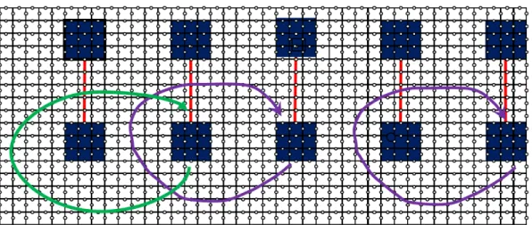
Meanwhile, surface code is another a way to encode logical qubits for topological quan-tum computation [16], [17], [18], [19]. Figure 2.5 shows an example of a lattice of physical qubits in which each white circle represents a physical qubit. The dark blue squares corre-spond to a defect, and a pair of defects connected with red lines represents logical qubits.
Figure 2.5: Logical qubits with braiding operations.
Green and purple lines show braiding operations conceptually. As one can see, a braiding operation is a movement of the status of a defect, and it can be assumed that multiple braid-ing operations can be done at the same time if their correspondbraid-ing lines do not overlap in the physical space as pointed out in previous section. Thus, in the figure, the two braiding operations corresponding to two purple lines can be done in one logical time step. Also, in Fig. 2.5, all the defects are of the same type (say, primal) and the other type defects (not
shown) are offset by a 1/2 defect size in both the vertical and horizontal directions. Here,
a logical CNOT gate can be achieved if a primal defect is braid around a dual defect.
2.2.4
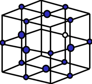
Logic circuit model for topological quantum computation
In a higher abstract model, the change of a defect status can be described as a strand, and a braiding can be expressed as a cross of two strands [12], [20]. Figure 2.6 shows a CNOT gate between two primal qubits. To perform a CNOT gate between them (as mentioned in
Figure 2.6: Braiding for a CNOT gate.
the previous section), the dual qubit is introduced here, as shown in the Fig. 2.6; a braiding of a dual strand (blue cuboid) is applied to the two primal strands (red cuboids) to perform a logic CNOT between the two primal qubits. The upper region of the geometry corresponds to the control qubit and the lower region corresponds to the target qubit.
A key to note here is for topological quantum computation, there is a recently pro-posed quantum circuit representation called ICM representation, which consists of qubit
(I)nitialization, (C)ontrolled-NOT gates and (M)easurements with respect to different bases [20].
More discussion about this quantum circuit representation will be given in Chapter 3. Therefore, with respect to the proposed ICM representation, the inputs are mapped on the left-hand side of the cuboids, and the outputs are mapped on the right-hand side. The time runs horizontally (from left to right) in the direction of the two primal strands.
Figure 2.7: Overlapped braiding operations.
2.2.5
Overlapped and non-overlapped braiding operations
First, see the example of braiding operations in Fig. 2.7. Note that a braiding operation between the logical qubits is denoted by a blue loop. For example, the left loop indicates
a CNOT gate between x1and x3and the right loop indicates a CNOT gate between x2and
x4. Thus, one can easily confirm that the two braiding operations for the two logical CNOT
gates are overlap in Fig. 2.7. Thus, the two gates must be performed in two logical time steps.
In contrast to the above, if the qubit order (qubit layout) is changed for this circuit, the both gates can be performed in parallel and thus a better implementation (Fig. 2.8) can be
obtained. Here the two circuits (Figs. 2.7 and 2.8) are logically equivalent but with different
qubit orders. To note here is that the time step can be reduced to half of the original circuit by changing the qubit order.
Figure 2.8: Non-overlapped braiding operations.
Two logical CNOT gates can clearly be done at the same time (in one logical time step) if their corresponding drawings in a quantum circuit do not overlap. (The definition of overlapped and non-overlapped for CNOT gates will be explained later in Chapter 5.) Therefore, the qubit order (qubit layout) is crucial for the computational time for topologi-cal quantum computation.
A key to note here is that multi-target CNOT gate braiding operations can also be per-form in a single braid. In other words, if gates with multiple target lines can be exploit, this will also help to reduce the time step computation. These reasons motivate this thesis to
Chapter 3
Design Methods for Topological
Quantum Circuits
The properties for topological quantum circuit model are significantly different from the
quantum circuit model even in the logic level; in topological quantum computation the logical primitive is called a braiding operation. In consequent to this unique property of topological quantum computation, to build a topological quantum computer requires a de-sign framework that can adapts with high level description of circuits. Accordingly, the
design strategy for topological quantum circuit should also be different from the quantum
circuit design.
The first part of this chapter discusses a design framework for topological quantum computation. Next section introduces a recently proposed quantum circuit representation called ICM representation, which consists of qubit (I)nitialization, (C)ontrolled-NOT gates
and (M)easurements with respect to different bases to support this design flow. The ICM
and replace them with exact gate lists that are robust against errors for a fault-tolerant
quan-tum computation. After that, this chapter introduces an efficient design flow for topological
quantum computation that incorporating with fault-tolerance and quantum error correc-tion, and compatible for a high level circuit description. Finally, Section 3.4 concludes this chapter.
3.1
Design framework for topological quantum
computa-tion
This section gives a summary of the design framework for topological quantum compu-tation which consists of four level that starts from the quantum algorithm level and ends at the physical hardware level. In between are the quantum circuit and the logical layer (geometric description) level; both are the most important steps for topological quantum computer framework. The first level of the design flow, quantum algorithm, is the most
ba-sic level/step to realize a quantum computer. The second level, quantum circuit, is used to
implement the quantum algorithm. This quantum circuit level is very important for topolog-ical quantum computation framework, thus there are many proposed optimization methods that aim especially for this level; these include optimization methods that targeting reduc-ing the circuit size, circuit depth and quantum cost for topological quantum computation circuit. The third level, logical layer, translates the optimized quantum circuit into geomet-ric representation. This level includes knowledge about physical layouts. Finally, the final
level, physical hardware, maps the geometric description to a physical hardware/quantum
3.1.1
Quantum algorithm level
A quantum algorithm that runs on a quantum computer can solve problems faster than a classical algorithm that runs on a conventional computer. Most widely known quantum algorithms are Shor’s Algorithm, Grover’s Algorithm, and Simon’s Algorithm [21], [22]. These algorithms are good models for a quantum computer as they have a potential to factor large numbers of information and achieve speed up in calculations, which are in contrast to conventional algorithms.
In general, many of the established quantum algorithms include a part to calculate Boolean functions corresponding to a problem instance; quantum algorithms usually
con-sist of common parts and unique parts [23]. Common parts do not differ for each problem
instance. On the other hand, unique parts differ for each problem instance. For
exam-ple, one of the famous quantum algorithms, Grover search algorithm [21], consists of the so-called oracle part and the other part. The oracle part is used to calculate a Boolean
function depending on a problem. Therefore, an efficient design technique for realization
of a Boolean function is crucial even for quantum circuits, as pointed out in the literature (e.g., [23]).
In order to achieve a full scale of quantum computer, the design of quantum algorithms have been greatly studied over the years by the researchers. Over the years many algorithms for reversible circuits have been introduced such as [24], [25]. Accordingly, it is also important to have promising models of computation that are compatible to work well with these large quantum algorithms. Among these models, topological quantum computation is one of the major discoveries that in principle allow a realization of large algorithms. Therefore, this thesis interests are mainly focused on this model of computation.
Later, the quantum algorithm is decomposed into quantum circuit. Thus, the next level, which is the quantum circuit level, is very crucial for topological quantum computation design framework.
3.1.2
Quantum circuit level
To implement a quantum algorithm we need to design a reversible/quantum circuit, and
in order to design a reversible circuit we need to use primitive reversible gates. Among
the existing reversible gates, Mixed Polarity Multiple-Control Toffoli (MPMCT) gates are
often used to implement a reversible circuit for Boolean functions. This is because the functionality of MPMCT gates naturally corresponds to AND-EXOR expressions. (More discussion in Chapter 4). Indeed, most existing researches generate an initial circuit con-sisting of MPMCT gates based on a small Exclusive-or Sum-Of-Product (ESOP) expres-sion [26], [27], [28]. Considering the functionality of MPMCT gates naturally corre-sponds to AND-EXOR expressions, this thesis gives more focus on this sort of reversible gate. An example of a quantum circuit is shown in Fig.3.1, which consists of gate set:
{Toffoli, CNOT, C − V, H, T}. The basic optimization in quantum circuits starts with
gen-erating an initial circuit. Once an initial circuit is obtained, further post-optimization tech-niques such as library-based, transformation-based and template-based optimization can be applied [29].
A natural question to ask when we design quantum circuits is how to evaluate the qual-ity of the circuits. To date, there are many proposed design methods for quantum circuit, therefore there is a need for a tool or a way of calculation to evaluate the quality of circuits of the proposed methods. The quantum cost is often used to evaluate the quality of the con-ventional quantum circuit. Therefore, there are many existing optimization methods that
Figure 3.1: An example of a quantum circuit.
aim to reduce the quantum cost for quantum circuits such as [30], [31], [32], [33], [34]. However, among the proposed optimization methods, there are only few known methods that are based on manipulating Exclusive-or Sum-Of-Products (ESOP) expressions to re-duce the quantum cost of the corresponding circuits. Therefore, one of this thesis main interests is on finding a method that can reduce the quantum cost by manipulating ESOP expressions. This thesis presents a totally new way for generating initial quantum circuits for Boolean functions with a reduced quantum cost. This technique involves adding Mixed
Polarity Multiple-Control Toffoli (MPMCT) gates to temporarily change the functionality
of the given function, so that the modified function has a smaller quantum cost. To compen-sate for the temporary change, additional gates are inserted into the circuit. The proposed method finds a small ESOP expression for the given function, and then finds a good pair of product terms in the ESOP expression so that the quantum cost can be reduced by applying the transformation. More discussion will be given in Chapter 4.
the next level of design flow, which is at the logical layer level.
3.1.3
Logical layer (geometric description) level
After optimizing the quantum circuit, each quantum gate is identified and is translated into its geometric representation. Figure 3.2 shows an example of a random quantum circuit that has been converted to a geometrical representation. In a geometric representation, each gate has a corresponding region of the 3D lattice, as previously mentioned in Chapter 2. In topological quantum computation, a large number of physical qubits are arranged in three-dimensional (3D) space in lattice as shown in Fig. 3.3, and a certain number of qubits on the same plane are used to express one logical qubit. Therefore, for topological quantum computation we can also arrange the qubits in two-dimension, not only in one-dimension of qubits arrangement like the quantum circuit in the conventional computer model.
One of the ongoing questions among the researchers is how to build a large-scale of
quantum computation that can efficiently implements quantum properties in its operations.
This is because a quantum information is quickly lost due to errors such as an interference of decoherence during the operations. One of the solutions for us to avoid any information lost or leak while performing operations is we have to ensure that a minimum distance between defects have to be satisfied. Thus, this gives researchers more distinct options to minimize the volume (size of space and time for computation) of physical hardware computation. Hence, it is very important to pay an extra attention to the logical layer level because this level is responsible for how qubit layout should be arranged within the lattice in the quantum physical hardware [35]. With this in mind, in order to optimize this
level, it is crucial to have an efficient method that can significantly reduce the total time
physical qubits and the computational time required to implement the circuit. Therefore, as pointed out in Chapter 2, if one can exploit the braiding operations and finds gates that can be arranged in parallel, it is possible to reduce the computational time step. Therefore, there has been a research to find a good qubit order in one-dimensional qubit layouts for topological quantum computation [13]. In contrast to this, this thesis introduces a two-dimensional qubit layouts for topological quantum circuit unlike the one-two-dimensional qubit layout that is often used in conventional quantum circuit. More discussion will be given in Chapter 5.
Later, once the quantum circuits have been translated to their geometric description, they are sent to the physical hardware.
3.1.4
Quantum physical hardware level
The final level of topological computation design flow is the physical hardware; here the geometric description obtained from the logical layer level is mapped to the physical hard-ware. Physical hardware level is responsible for specifying the measurements on physical qubits and determining layouts for the physical qubits in the 3-dimensional lattice. This means that this level is very important for determining the final physical volume of topolog-ical quantum circuit. An optimization for mapping topologtopolog-ical quantum circuits to phystopolog-ical hardware can be found in [35]. A key to note here is in order to minimize the size of phys-ical hardware, one of the best strategies is to get a small volume of geometric description derived from the logical layer level. Thus, in corresponds to the one of the best strategies, this thesis gives more focus on optimizations at the logical layer level.
Figure 3.2: An example of a geometrical representation converted from a quantum circuit.
Figure 3.3: 3-Dimensional lattice of qubits.
3.2
An approach to support topological quantum
compu-tation design flow
For topological quantum computation, there is a recently proposed quantum circuit repre-sentation called ICM reprerepre-sentation, which consists of qubit (I)nitialization,
(C)ontrolled-NOT gates and (M)easurements with respect to different bases [20]. Any quantum circuits
consisting of any quantum gates (e.g., controlled-V, Toffoli gates) can be transformed into
ICM representation after decomposing all the non-deterministic gates with an exact gate list that are robust against errors. After the decomposition, all the qubit initializations are moved to the beginning of the circuit, all the single-qubit measurements are moved to the end of the circuits, and the CNOT gates remain in the middle of the circuits.
The purpose of ICM is to create a deterministic circuit from probabilistic components (e.g., measurements) and these quantum operations are relatively robust. Note, the middle part of the ICM representation consists of many CNOT gates for a practical computation. Thus, we need to consider how to design a circuit that consists of only CNOT gates for the realization of topological quantum computation. More discussion will be given in Chap-ter 5.
This section explains how to perform fault- tolerant topological quantum computation based on ICM representation. To obtain ICM representation, first all the non-deterministic
gates (non-UGSf t gates) need to be decomposed into a fault-tolerant quantum computing
set: UGSf t= {CNOT, H, T}. The design flow for ICM representation follows these three
steps:
Step 1: Approximation
• Arbitrary circuits can be realized by two possible gates sets: finite (e.g., Clifford + T) or infinite (containing arbitrary angle rotations that require an approxima-tion sequence).
• At this step, for finite sets, no approximation is needed because the complexity of the ICM transformation algorithm is linear for the number of gates in an input circuit. However, in the case of infinite sets, should need an approximation first. • At the same time, the decomposition database, which includes gate decomposi-tion of ICM or non-ICM, is loaded. This database stores corresponding circuits that match the gates to be decomposed.
• The compiling processes for finite and infinite gate sets are different. Infinite gate sets require further transformation into an intermediate circuit composed of gates from the finite universal gate set.
• At this step, the intermediate gates (gates after the approximation step) are fur-ther decomposed into ICM representation.
• At the same time, the decomposition database, which includes the gate decom-position of ICM or non-ICM, is also loaded (similar step to approximation). This database stores corresponding circuits that match the gates to be decom-posed.
• The resulting ICM circuit includes a qubit initialization list, CNOT gate list, and a measurement list. All the ancillas initialization are moved to the beginning of the circuits, and the qubit measurements are moved to the end of the circuit, leaving only the middle of the circuits with CNOT gates.
Step 3: Canonical geometry construction
• The resulting ICM circuit description (including a qubit initialization list, a CNOT gate list, and a measurement gate list) can be visualized by a canonical geometric description, which is a three-dimensional bijective mapping of the circuit description.
• The geometric description consists of three geometric regions that map the ini-tialization, the CNOT, and the measurement, similar to the circuit description.
For greater understanding of this design flow, lets see an example on how to trans-form an arbitrary circuit (Fig.3.1) into an ICM trans-form of the structure. The circuit in Fig.3.1
consists of gate set: {Toffoli, CNOT, C − V, H, T}. At the approximation step, the decom-position database, which stores the corresponding circuit that matches the gates to be
de-composed, is loaded. The database decomposition includes ICM and non-ICM (non UGSf t
= {CNOT, H, T}) gate decomposition. Thus, for example, at this step a Toffoli gate which is a non-ICM gates is loaded from the database.
During this step, the non-ICM gates of the Toffoli gate is decomposed into single qubit
rotations (either {V, V†} or {H, T, T †}, and the Hadamard gate is replaced with a series of Z- and X- axis rotational gates (P and V gates).
At the compilation step, the circuit is further decomposed into ICM representation. Similar to the approximation step, here the decomposition database, which stores the cor-responding circuit that matches the gates to be decomposed, is loaded. The ICM decom-position for the T gate and the controlled-V are loaded and the ancillas are introduced. After the compilation, the resulting circuit description includes a qubit initialization list, a CNOT gate list, and a measurement gate list that matches the ICM form of the structure. For example, see Fig. 3.4.
Figure 3.4 shows the ICM representation of a controlled-V gate taken from a previous work [36]. After the compilation, the ICM representation for a controlled-V gate has
in-puts states cin (control) and tin and outputs cout and tout. The size of the circuit expands
significantly due to the increased ancillas. All the ancillas initialization are moved to the beginning of the circuit and single qubit measurement are moved to the end of the circuit. The middle of the circuit is now left with CNOT gates only, proving that ICM representa-tion replaces the non-deterministic gates with an exact gate list.
As for the last step, each single logical qubit operation can be visualized into a geo-metrical description, where each property of the circuit description elements has a single
Figure 3.4: ICM representation of a controlled-V gate.
corresponding structure to the geometric description (see an example in Fig. 2.6). As
pre-viously explained, the logical qubits are defined as strands/defects here.
3.3
Design flow for topological quantum computation
This section proposes a design flow for topological quantum computation (which is also incorporating with all necessary fault-tolerance protocols) as illustrated in the following.
The proposed design flow consists of four important steps as illustrated in Fig. 3.5; note
this design flow is very different from the conventional quantum circuit design.
At step 1, a quantum algorithm is decomposed into a high level of quantum circuit; this step is the most required step for any proposed design flow for topological quantum com-putation [35]. At this step, a quantum algorithm such as Shor algorithm is transformed into a quantum circuit, which consisting of quantum gates such as NOT gates, CNOT gates, and
Toffoli gates. At step 2, the quantum circuit obtained from step 1 is transformed into ICM
circuit of representation. The ICM circuit of representation provides an exact gate list that are robust against errors after decomposing all the non-deterministic gates. This allows a better starting point before further optimizations at the logical layer level and the physical hardware level. After that, at step 3, each gates resulting from step 2 is identified and log-ically encoded with the topological codes before translated into its geometric description. Here, each gate has a corresponding region of the 3-dimensional lattice as mentioned in the previous chapter; each logical qubit is encoded as two defects on a lattice of physical qubit. Finally, at step 4, once the decomposition of the translated geometric description is complete, they are sent to the physical hardware.
3.4
Conclusion
This chapter presented a design framework for topological quantum computation and an approach to support the proposed design flow. Later, Chapter 4 and Chapter 5 discuss the proposed optimization methods for the quantum circuit level and the logical layer level by using this design framework for topological quantum computation.
Chapter 4
Reducing Quantum Cost for Topological
Quantum Circuits
Quantum cost is often used as the most general way to evaluate the quality of reversible or quantum circuits in the conventional quantum circuit model [37], [38], [39]. Existing opti-mization methods often use template matching to minimize the gate count in order to find the possible cost reduction [40], [41]. In contrast to the existing methods, this thesis pro-poses a totally new technique for generating initial quantum circuits for Boolean functions with reduced quantum cost by making temporary changes to the functionality of a given Boolean function. This technique is one of the very few known methods based on manip-ulating Exclusive-or Sum-Of-Products (ESOP) expressions to reduce the quantum cost of the corresponding circuit [42]. The proposed method attempts to make temporary changes to the original function by adding some MPMCT gates, so that the changed function leads to a smaller quantum circuit. Then, the proposed method evaluates a “good” temporary changes and picks the one that reduces the total quantum cost, including the additional
MPMCT gates, as much as possible. Further, based on the idea, this thesis proposes an iterative heuristic method to reduce the quantum cost for practical (i.e., large) circuits. This technique is of a particular interest since it can be considered as a good pre-optimization
methodto make temporary changes to the given function, unlike the existing methods that
keep the function unchanged.
The first part of this chapter discusses how to realize Boolean function with MPMCT gates and how to design a reversible circuit by minimizing ESOP expressions. In the next section, this thesis reviews a design method proposed by Arabzadeh et. al.; Arabzadeh method can find a circuit with a low quantum cost by minimizing ESOP expressions using rules applied to a Karnaugh map [26]. After that, the next section explains the general idea of the proposed method, and shows that the proposed approach can find more cost reduction than the Arabzadeh method. To implement the idea for practical (i.e., large) circuits, an iterative heuristic method is introduced in Section 4.4, and the next section shows the experimental results of the proposed method. Finally, Section 4.6 concludes the discussion.
4.1
Realizing Boolean function with MPMCT gates
Like most of the existing design methods, this thesis considers the model of reversible circuits for calculating Boolean functions as shown in Fig. 4.1. More formally, the circuit model used in this thesis is as follows:
• There are n input variables, x1, · · · , xn, whose states should not be changed.
• There is one target bit, t, used to calculate a target Boolean function f (x1, · · · , xn) as
Figure 4.1: Reversible circuit model.
This thesis imposes the above restrictions because they are necessary for a reversible circuit to be used in existing quantum algorithms which utilize the so-called quantum interference. A minterm of a Boolean function is the combination of values (negative or positive) of all the input variables such that the Boolean function evaluates to 1 on this combination. In
the following, an MPMCTngate means an MPMCT gate that has n control bits.
To realize an n-input Boolean function with k minterms by a reversible circuit, it is
possible to use k MPMCTn gates such that;
(1) Each MPMCTngate corresponds to each minterm of the function.
(2) The polarity of each control bit for an MPMCT gate corresponds to each variable’s polarity in the corresponding minterm.
In other words, if xi or xiappears in a minterm, the corresponding control bit is positive or
negative, respectively. In this construction, the target bit of all the MPMCTn gates is the
Table 4.1: A truth table for a 4-input Boolean function with 4 minterms.
x
1x
2x
3x
4f
(x)
0
0
0
0
0
0
0
0
1
0
0
0
1
0
0
0
0
1
1
0
0
1
0
0
0
0
1
0
1
1
0
1
1
0
1
0
1
1
1
0
1
0
0
0
0
1
0
0
1
1
1
0
1
0
1
1
0
1
1
0
1
1
0
0
0
1
1
0
1
0
1
1
1
0
0
1
1
1
1
0
For instance, Table 4.1 shows a 4-input Boolean function with 4 minterms, and the circuit in Fig. 4.2 realizes the function: x2· x4· x1· x3⊕ x2· x3· x1· x4⊕ x1· x4· x2· x3⊕ x1· x3· x2· x4.
For example, the left-most gate in Fig. 4.2 corresponds to x2· x4· x1· x3; the control bits
for x2and x4 are in the positive polarities denoted by black circles, and x1and x3are in the
Figure 4.2: The quantum circuit for Table 4.1.
4.2
Initial circuit generation by minimizing ESOP
expres-sions
Most optimization methods use template matching to find any possible cost reduction in re-versible or quantum circuits [40], [41]. Unlike the existing methods, the proposed method in this thesis attempts to make temporary changes to the original function by adding some MPMCT gates, so that the changed function leads to a smaller quantum circuit, or in other words, leads to a circuit with a lower quantum cost. Thus, in order to understand the con-tribution of this chapter it is beneficial to understand how to design a reversible circuit by minimizing ESOP expressions. For that purpose, in the following, this thesis reviews a design method proposed by Arabzadeh et. al. [26]. Their method can find a circuit with a low quantum cost by minimizing ESOP expressions using the rules applied to a Karnaugh map (a Kmap, hereafter).
A Kmap for a Boolean function is a two-dimensional arrangement of cells where each cell has the corresponding output value (“1” or “0”) of the Boolean function. In a Kmap, one often omit “0” for simplicity. For example, the leftmost diagram in Fig. 4.3 shows a Kmap for the function: x1x2x3x4⊕ x1x2x3x4⊕ x1x2x3x4⊕ x1x2x3x4. The cell at the second row
from the top and the second column from the left corresponds to the function value when (x1, x2, x3, x4)= (0, 1, 0, 1). Each cell having 1 corresponds to one minterm in the function.
A Kmap is very useful for simplifying a Boolean expression because one can determine which minterms should be combined from the positional relationship of corresponding cells in the Kmap. For example, the rectangular shape of adjacent four cells in the leftmost
diagram in Fig. 4.3 means that one can get the simple expression: x2x4 for the function.
Kmap. Also, a cell having the 1 value is called 1-value cell. For a minterm with n input
variables, it can be expressed as one MPMCTn gate. Also, one 1-value cell corresponds
to one minterm in a Boolean function. Therefore, in a Kmap for an n-input function, one
1-value cell corresponds to one MPMCTngate.
In the conventional logic design, one can optimize a two-level AND/OR/NOT
expres-sion of a function by manipulating the Kmap for the function with some rules. Arabzadeh
et. al. proposed a similar optimization method for quantum circuits based on Kmaps [26];
this method is referred to as the Arabzadeh method in this thesis. In the Arabzadeh method, they apply the so-called CTRs (Common-Target Rules) to quantum circuits; the rules are stated as follows.
(a) All 1-value cells should at least belong to one group of cells.
(b) Each group has a size of 2p(p ≥ 0) .
(c) Each group should have a maximum size.
(d) Each 1-value cell should belong to an odd number of groups.
(e) Each 0-value cell should belong to an even number of groups.
(f) The number of groups should be minimum (as much as possible).
A group is a collection of cells that are next to each other, and denoted by a rectangle on a Kmap. The above rules indicate that 0-value cells can also be covered when consid-ering the optimization of a quantum circuit; this is in contrast to the case of a two-level
A group in a Kmap is used to optimize a part of an expression of a certain Boolean
function. For instance, 2p(p ≥ 0) cells correspond to 2p MPMCTngates; if they can be in
one group of 2p (p ≥ 0) cells, the 2p
MPMCTn gates can be optimized to become a single
MPMCTn−pgate. Thus, the quantum cost can be reduced drastically.
Figure 4.3 shows how this rule is applied to optimize a circuit. The four leftmost cells in a Kmap in Fig. 4.3 belong to a group that can be described as x1x2x3x4 ⊕ x1x2x3x4 ⊕
x1x2x3x4⊕ x1x2x3x4. This corresponds to the circuit that has four MPMCT4 gates in the
middle of the same figure. After the optimization by using the above rules, the function can
be optimized to x2x4, and thus the optimized circuit on the right of the same figure can be
obtained. By looking up the quantum cost listed in the literature [43], the quantum cost is reduced from 80 to only 5 in this example.
In short, the quantum cost can be reduced by eliminating more control bits of MPMCT
gates in a circuit. When the size of a group (of adjacent cells) is 2p, the ratio of the number
of gates after optimization to the number of gates before optimization becomes 21p. Also,
the ratio of the number of control bits after optimization to the number of control bits before
optimization becomes n−pn . Thus, when the size of a group (of adjacent cells) is large, one
can reduce the quantum cost by using the above optimization strategy.
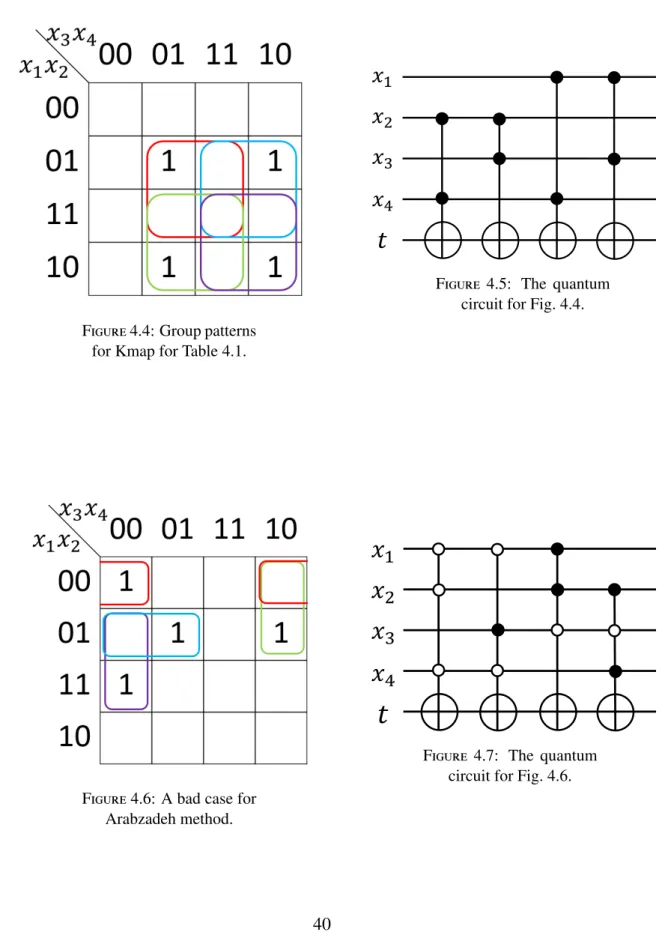
For the Boolean function shown in Table 4.1, if one make groups using a Kmap as shown in Fig. 4.4, the resulting quantum circuit as shown in Fig. 4.5 can be realized. In the above example, the quantum cost is reduced from 80 to 20. Thus, in most cases, the quantum cost can be reduced by using the Arabzadeh method. The next section discusses another way to reduce the quantum cost; the proposed method can reduce the cost of the same example to only 9.
Figure 4.4: Group patterns for Kmap for Table 4.1.
Figure 4.5: The quantum circuit for Fig. 4.4.
Figure 4.6: A bad case for Arabzadeh method.
Figure 4.7: The quantum circuit for Fig. 4.6.
4.3
A pre-optimization technique to reduce quantum costs
4.3.1
General idea and a motivational example
It was shown in the previous section that the Arabzadeh method can find a circuit with a low quantum cost by minimizing ESOP expressions using the rule applied to a Kmap. However, when utilizes the Arabzadeh method, the location of each 1-value cell in the Kmap always stays at the initial point as in a given Boolean function. It seems to be natural to do so, but the initial locations of 1-value cells may cause bad results in some cases.
For example, for a Kmap shown in Fig. 4.6, the method can only generate the cir-cuit as shown in Fig. 4.7; this thesis can find a much better circir-cuit by the proposed pre-optimization technique as follows. The proposal involves moving 1-value cells so that the resulting Kmap can be implemented by a reversible circuit with a much lower quantum cost. In order to do so, MPMCT gates are added to the initial quantum circuit. Note that inserting MPMCT gates changes the functionality of the quantum circuit. Therefore, the
corresponding MPMCT gates are also added at the end in order to cancel the effect so that
one can have the desired functionality, as shown below.
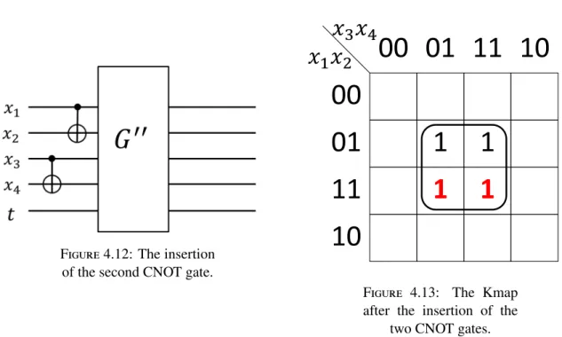
The following example explains what is mean by “inserting an MPMCT gate”. Let G be a quantum circuit realizing the Boolean function shown in Table 4.1. In the proposed
method, an MPMCT gate whose positive control bit is x3and the target bit is x4(i.e., CNOT
gate) is inserted before G0 as shown in Fig. 4.8. The idea is as follows: if one implement
a circuit G0 whose Kmap is shown in Fig. 4.9, the entire circuit (i.e., G0 with the inserted
CNOT) realizes the original function of (G) whose Kmap is shown in Fig. 4.10.
The reason is as follows: the inserted CNOT (the control bit is x3 and the target bit is
Figure 4.8: Insertion of a CNOT gate before G0.
ϬϬ Ϭϭ ϭϭ ϭϬ
ϬϬ
Ϭϭ
ϭ
ϭ
ϭϭ
ϭϬ
ϭ
ϭ
Figure 4.9: The Kmap af-ter the insertion of the first
CNOT gate.
ϬϬ Ϭϭ ϭϭ ϭϬ
ϬϬ
Ϭϭ
ϭ
ϭ
ϭϭ
ϭϬ
ϭ
ϭ
Figure 4.10: The Kmap before the insertion of the
first gate.
ϬϬ Ϭϭ ϭϭ ϭϬ
ϬϬ
Ϭϭ
ϭ
ϭ
ϭϭ
ϭϬ
ϭ
ϭ
Figure 4.11: The move-ment of cells by the in-sertion of the first CNOT
Figure 4.12: The insertion of the second CNOT gate.
ϬϬ Ϭϭ ϭϭ ϭϬ
ϬϬ
Ϭϭ
ϭ
ϭ
ϭϭ
ϭ
ϭ
ϭϬ
Figure 4.13: The Kmap after the insertion of the
two CNOT gates.
(x1, x2, x3, x4) = (0110) to (0111), for example. Also, the gate moves (1010) to (1011).
More precisely, the gate swaps four pairs of cells in a Kmap, as shown in Fig. 4.11.
There-fore, it can conclude that by inserting the gate, it is enough for G0to realize the function as
shown in Fig. 4.9. In this case, the desired function will be realized as shown in Fig. 4.10. Similarly, if one insert the second CNOT gate as shown in Fig. 4.12, the sub-circuit
G00 in Fig. 4.12 should realize the function whose Kmap is as shown in Fig. 4.13. This is
because the second gate moves the minterm (1001) to (1101), and (1011) to (1111). Thus,
G00should implement the function in Fig. 4.13, which can be done using one Toffoli gate.
Note that the resulting states of qubits after the circuit in Fig. 4.12 are not exactly the
same as the ones in the desired circuit shown in Fig. 4.5, because the functionality of x2
and x4 are changed by inserting the two MPMCT gates. Therefore, the matching MPMCT
gates after G00are inserted at the end of the circuit, as shown in Fig. 4.14.
Figure 4.14: The insertion of two CNOT gates to re-store the original function.
Figure 4.15: The final quantum circuit by the proposed method: Cost 9.
should be noted that by simply use the Arabzadeh method only it is possible to get a circuit with a quantum cost of 20 for this example.
4.3.2
How to insert MPMCT gates for a good pre-optimization
The above-mentioned example shows that there is a case where inserting some MPMCT gates improves the quantum cost drastically. As explained in the previous section, inserting an MPMCT gate corresponds to the movement of 1-value cells in a Kmap, i.e., changing the specification of a given function. Thus, such a change of the specification can be considered as pre-optimization before generating a quantum circuit.
For simplicity, considers an n-input function having k (= 2p) 1-value cells here. If k is
small, it is possible to try all the possible movements of 1-value cells as follows.
• Select one cell from all the k 1-value cells, and move all the other 1-value cells so that all k 1-value cells form a group of adjacent cells. As a result, the function is
changed so that it can be realized using only one MPMCT(n−p) gate.
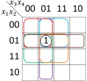
First there is k possibilities to select one 1-value cell which do not move. For
exam-ple, let considers a cell denoted by 1 in Fig. 4.16 for the selected 1-value cell. Then,
for the selected 1-value cell, considers nCp groups of k(= 2p) adjacent cells
corre-sponding to product terms with n − p literals of a n-variable function. As Fig. 4.16
shows, there are 6 (= 4C2) such groups in this example where n = 4, p = 2, k = 4.
Select one group from thenCp groups, and then move other k − 1 cells into the
se-lected group of cells. There is (k − 1)! of choices to move which 1-value cell to which
cells in the group. For example, in Fig. 4.17, 1 is the selected 1-value cell and the
dotted area is the selected group of cells; move k − 1(= 3) cells as the figure shows,
and one have (k − 1)! possibilities of such movements. Thus, in total, all the possible movements is k ×nCp× (k − 1)!, which is equals to (k)! ×nCp.
Thus, if this number is not large, one can try all the possible movements to find the best movement corresponding to the best insertion of MPMCT gates with the lowest quantum cost.
The experimental results demonstrate that the above idea is potentially useful by
con-sidering a small function with n = 4 and k = 4 in Section 4.5. However, obviously, the
above exhaustive search is not applicable to practical (i.e., large) functions; the next section proposes heuristic method for large functions.
4.4
Proposed heuristic method
In the previous section, an optimization method by inserting an MPMCT gate was intro-duced; the method results in reduction of quantum cost. To put it in another way, it would be a unique idea to make temporary changes to the functionality of a given Boolean function
Figure 4.16: Various grouping of adjacent cells for a product term
with two literals.
Figure 4.17: An example of moving 1-value cells.
such that the modified function has a small ESOP expression, which results in a quantum circuit with reduced quantum cost. However, in order to utilize the idea for large practical functions, one have to come up with an excellent heuristic approach to avoid the above-mentioned exhaustive search. Therefore, this section presents a heuristic approach to solve this problem.
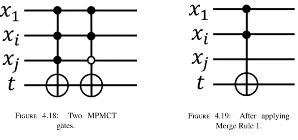
First, the following “Merge Rules” are introduced here. The quantum cost can be re-duced by merging a pair of MPMCT gates, by using the following “Merge Rules”.
Merge Rule 1
If two MPMCT gates A and B have the same control bits and the same target bit but the
polarity of only one control bit is different (i.e., negative and positive), then the two gates
can be merged into one MPMCT gate.

![Table 4.2 shows the comparison between the proposed method and the method based on the ESOP minimization by EXORCISM4 [44]](https://thumb-ap.123doks.com/thumbv2/123deta/6578610.1133731/70.892.173.705.203.435/table-shows-comparison-proposed-method-method-minimization-exorcism.webp)
