3
Trends of Research and Development in Semiconductor Manufacturing Technologies
– From Presentations
at Recent International Conferences*1 and Other Sources –
HIROSHI KOMATSU
Information and Communications Research Unit
1 Introduction
Despite technical and economic limitations, t he pace of de velopment of si l icon MO S semiconductor technology is accelerating. LSI chips are acquiring more complex and versatile functions by incorporating even radio-frequency and analog technologies inside that were thought too difficult for silicon MOS devices in the past.
Increasingly, semiconductor devices will be used in a variety of products, including commonplace commodities. Semiconductor technology will continue to be the fundamental technology s uppor t i ng t he de velopme nt of not on l y electronics but also basic science and technology.
Economically speaking, it should play a major role in key industries.
This repor t will sur vey recent trends in research and development of semiconductor t e c h n ol o g y, fo c u s i n g o n t h e u n d e r l y i n g manu facturing technologies, and will also touch br ief ly on t he ch a l lenges faced by semiconductor-related projects in Japan.
2 Development of next
generation MOS transistors
2-1 Development of MOS transistors is in transition
A transistor usually works as a switch in digital circuits by changing its status between “on” and
“off”. A key type of transistor that has supported the technical revolution of semiconductor integrated circuitry is a unipolar transistor*2 with
a structure called MOS (Metal-Oxide-Semiconduc tor, see Figure 1).
The basic materials and structure of MOS transistors*3 have not changed much since their beginnings, as far back as 1970. The MOS tr a nsistor uses a conductor made of polycr ystalline silicon*4 doped with a high concentration of impurities, a silicon dioxide film (SiO2) made by thermal oxidation of single-crystal silicon, and single crystal silicon, for metal, oxide and semiconductor, respectively. In spite of the MOS name, the major elements in an MOS transistor are just silicon and oxygen, the two most abundant elements on Earth.
A f ter t he ba sic mater ia ls a nd str uct u re o f M O S t r a n s i s t o r s w e r e d e t e r m i n e d , semiconductor manufacturing technology saw a new generation emerging every three years, thanks to lower defect densities in silicon crystals, higher purification of other materials and miniaturization technologies. Advances in fine patterning and accurate processing by lithography have enabled the continuous improvement of LSI integration, as can be seen in Figure 1: Basic materials and structure of silicon MOS
transistor
DRAMs.
In the 1990s, the issues were how to cope with parasitic effects such as increased resistance and capacitance caused by the miniaturization of transistors and connections within LSIs.
The following materials or structures were introduced separately to reduce these effects. (1) A compound of silicon and a metal (silicide or metal-silicide), (2) New materials such as copper (Cu)*5, and (3) a partially new structure like SOI*6.
But recently we have a r r ived at a stage where further miniaturization of transistors by conventional methods does not necessarily promise additional performance enhancement.
For example, when the gate oxide becomes too thin, it does not work as an insulator any more and gate leakage current increases.
The issues and problems above are forcing the reexamination of the conventional materials and structures of transistors that have brought us to this point.
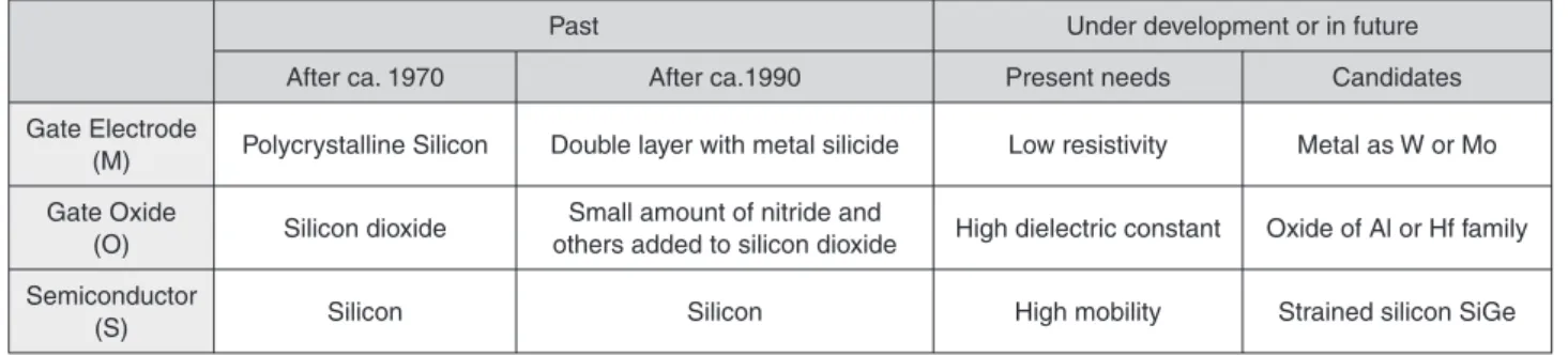
The response is the recent aggressive research and evaluation of new materials, as shown in Table 1. The central focus for the gate electrode is the use of metallic materials with lower resistivity. Examples include tungsten (W) and molybdenum (Mo), which have lower resistivity than polycr ystalline silicon and can endure the high temperatures encountered during the manufacture of semiconductors. For the gate oxide, high dielectric constant films are evaluated, as high electric field can be applied at lower voltages, resulting in lower leakage current from the gate electrode. Examples are oxides of aluminum (Al), hafnium (Hf) and others. For the semiconductor, re-investigation is focused on high-mobility materials that have faster charge carriers than those in conventional silicon. Some examples are strained silicon and a compound of silicon and germanium (SiGe).
As for transistor structure, a new transistor with multiple-gate electrode is being investigated, in contrast to a conventional transistor, which is planar and has a single-gate electrode. The goal of the investigation is to improve controllability of the electric field*7 through the gate electrode and create a transistor with excellent on/off switching characteristics. Examples of this are the double- gate transistor, and the tri- gate or fin-type transistor, as shown in Figure 2. The electric field in the channel region will be better controlled if the gate electrode is attached to the region from not just a single side, but from two or three, or even if the electrode surrounds all sides of the region. New MOS transistor structures aim at this effect.
2-2 Evaluation status of new materials and structures
(1) High-k (high dielectric constant) insulating film
U n t i l a r o u n d t h e y e a r 2 0 0 0 , v a r i o u s compounds*8 were candidates for high-k (high dielectric constant) film materials, and various formation methods were discussed. The hafnium oxide group looks most promising, due to its dielectric constant and thermal stability. At IEDM2003*9, “Hf-based Gate Dielectrics” was the only session on high-k insulating films, which Table 1:Evolution of MOS transistor materials
Past Under development or in future
After ca. 1970 After ca.1990 Present needs Candidates
Gate Electrode
(M) Polycrystalline Silicon Double layer with metal silicide Low resistivity Metal as W or Mo Gate Oxide
(O) Silicon dioxide Small amount of nitride and
others added to silicon dioxide High dielectric constant Oxide of Al or Hf family Semiconductor
(S) Silicon Silicon High mobility Strained silicon SiGe
Figure 2:Structure of multigate transistors
is good evidence that the material selection is being narrowed down. The thin film formation method called ALD (Atomic Layer Deposition), that deposits films layer by layer in atomic or molecular status, is moving into the mainstream.
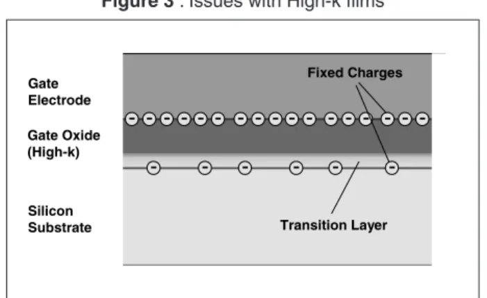
At first it was thought that optimization of h ig h - k f i l m pr op e r t ie s shou ld le ad to better transistor characteristics. However, as is described in next paragraph, during the investigation of the application of this technology to real devices, it became clear that simple replacement of the dielectric with the high-k film, while it improves the dielectric constant, also leads to overall degradation of device performance.
The problem initially encountered was a reduction of carrier mobility by around 50%[1]
due to transition layers and fixed charges located at the interface with the silicon substrate, or by lattice scattering caused by polarized bonds called soft phonons that are peculiar to high-k films. This leads directly to the degradation of device performance and has to be fixed before the adoption of high-k films. At a VLSI symposiu m held i n 20 03, it was repor ted that mobility of up to 80 - 90% of the level of conventional film can be recovered[2] if nitrided hafnium silicate (HfSiON) film is plasma oxidized or plasma nitrided after the film deposition.
However, at the same VLSI symposium, another report said that fixed charges generated at the interface between polycrystalline silicon and high-k film prevent the control of the transistor threshold voltage by the channel impurit y concentration and the capacitance of the gate insulator. This reconfirms the difficulty of bringing high-k film into mass production[3]. In other words, conventional silicon dioxide has ideal interface properties.
High-k films also present reliability issues, as was recently pointed out[4]. Some examples are the change of film properties when an electrical field is continuously applied, and degradation of the film properties by injection of some portion of high energy electrons or holes into the high-k film from the channel under prolonged use.
S i l i c o n d i ox i d e f i l m s h a v e b e e n u s e d extensively, and there is abundant and cumulative information concerning the changes undergone
by gate dioxides after long hours of use. For high - k films, on the other hand, discussion of reliability data has just begun. Whenever new issues concerning high-k films are raised, the view gains more ground that replacing silicon dioxide with other materials is not so easy. Silicon dioxide has gone through many improvements in film formation technologies in the past and has reached its ultimate thickness - or thinness - at about 1 nm. Still, Intel and AMD have announced[5,6] that high-k film along with a new gate metal will be adopted for the 45 nm generation to be shipped in 2007.
(2) Strained silicon
The strained-silicon MOS transistor has entered the limelight since two papers[7,8] on it were submitted by IBM at the VLSI Symposium in 2001. Strained-silicon technology adds tensile or compressive strain to the channel region in order to increase carrier mobility, which is one of the characteristic of a substrate material. It was generally expected that its mass production would begin after 2005 at the earliest, which was IBM’s own view.
However, i n 2 0 02 I ntel a n nou nced t he application of strained - silicon technology to the Pentium 4 beginning in 2003. Also in 2002, AmberWave Systems*10 in the U.S. was reported to be preparing for licensed sales of strained-silicon substrate technology[9]. These developments quickly intensified the limelight on the technology.
In the CMOS device session of IEDM2003, there were many presentations on strained silicon that drew much attention, including a posting to the Late News*11 from Intel. A dozen papers were presented at IEDM2003 on strained silicon,
Figure 3 : Issues with High-k films
including those in the late news. The subject was addressed in about 40% of the entire 30 papers presented in the CMOS session. It seems that interest in the development of next-generation transistors has recently focused on strained silicon and on the multigate transistor that will be discussed in the next section.
W hat Intel announced[10 ] is independent optimization of silicon strains in NMOS and PMOS channel regions by applying mechanical stress separately to each area, with adequate control. As this applies strain only locally to channel regions, it may not really constitute a change of the basic materials of the MOS transistor underneath the gate electrode. But this technology is noteworthy as it is being applied to the first product of the 90 nm generation, the Pentium 4, with only a 1 - 2 % increase in its manufacturing cost.
(3) Multigate structure
For some time, a double - gate structure has been investigated in combination with an SOI structure. In the past few years there has been much more active interest in a tri-gate structure whose channel region is covered by the gate electrode from three sides and that can only be fabricated by vertical processing onto the substrate. The tri-gate transistor is often called a “FinFET” especially when the gate electrode is formed well underneath the semiconductor substrate as shown in the bottom drawing of tri-gate structure in Figure 2 below.
FinFETs can be fabricated fairly easily only by processing from the direction vertical to the substrate, and six papers on the concept were presented at IEDM2002 by IBM and others.
Fin-FETs give an easy performance improvement while suppressing the side effects that accompany miniaturization. But at IEDM2003, the number of papers on the technology went down to 2, because FinFET requires the formation of near 3 - dimensional deep patterns on the substrate, though processing itself can be performed only from the direction vertical to the substrate, and because wiring connection to the FinFET was difficult. This indicates that the hot interest in this transistor structure quickly cooled and the focus shifted to strained-silicon technology.
A M D a n nou nced a tr i - gate tr a nsistor at SSDM2003 (2003 International Conference on Solid State Devices and Materials) held in September 2003. In this transistor, with its channel region surrounded by metal gate on three sides (as shown in the top of tri-gate structure drawings in Figure 2), they deformed the silicon lattice locally and enhanced carrier mobility. By covering three sides with the gate electrode, the effective channel width is increased and better controllability of on/off switching is obtained, leading to improved transistor performance. The structure is closer in shape to a planar transistor as its metal electrode is formed only shallowly into the substrate, and it is more compatible with conventional processes.
The GAA (Gate All Around) type transistor that has its channel region surrounded by gate electrode on all sides is called an ultimate MOS structure. But the structure presents difficulties for higher integration with MOS processing, and its performance is under evaluation mainly with vertical MOS structures[11] where current flows perpendicular to the semiconductor surface.
Recently, investigation of GAA structure has begun on transistors whose channel is formed over carbon nano-tubes.
3 Number of papers accepted by IEDM
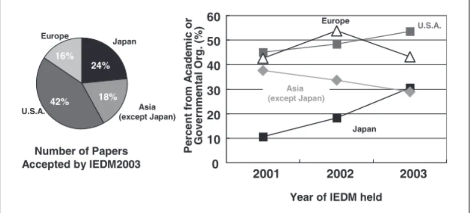
The pie chart to the left in Figure 4 shows the number of papers accepted by IEDM2003 by country or region of the author’s organization, and the right-hand side shows changes in the percent of papers coming from academic and governmental organizations for IEDM2001 - IEDM2003. Here, papers originating in multiple organizations are propor tionally allocated according to the organizations involved.
The distribution of the number of papers accepted by IEDM2003 by country and region is not significantly different over these few years[12]. Slightly less than half of the total were submitted from the U.S., about a quarter from Japan, and the rest from Asia (excluding Japan) and Europe.
In the past, papers from Japan were credited ma i n ly to i ndustr y, but with the cha nges i n progress si nce 20 01 the non - i ndustr ial
contribution is increasing. They came mainly from research organizations involved in national projects, and the contribution from universities was 10 - 15 %, with no significant change from 2001 or earlier.
Figure 5 shows the percent of papers accepted by IEDM from multiple authors of multiple organizations by country and by region in 3 recent years. It has already been pointed out that in Japan, not only cooperation between industry and universities, but also cooperation within industry itself or between universities is rather small compared with other countries or regions[13]. Actually, joint research in industry is increasing in Japan, reflecting the trend towards market reorganization and/or business alliances.
But the result of joint research projects with universities or governmental organizations is not yet visible, or at least not reflected in the number of accepted papers above. For example, the ratio of accepted papers from collaborations of universities and those with multiple research organizations involved is about 30% for Japan, 40% for the U.S. and 90% for Asia (excluding Japan) and Europe.
4 Semiconductor technology roadmap and technology development speed
T h e I T R S ( I n t e r n a t i o n a l Te c h n o l o g y Roadmap for Semiconductors)[14] identifies the technological needs facing the semiconductor industry over the next 15 years. The needs for lithography for example, include resolution and accuracy, overlay accuracy, and exposure area. In addition to lithography needs, the technological
needs for various areas like silicon wafers and each process step of semiconductor fabrication and assembly processes are listed there. The ITRS was targeted for U.S. domestic use when it originated in 1992, as the NTRS (N stood for National). Now, it has become international.
The contents of the ITRS are based on the consensus of participating specialists. In reality, as technology development is achieved ahead of ITRS requirements, its roadmap is moved up every time the ITRS is updated.
A s the pace of gener ationa l cha nge has apparently gone up recently, what was initially the “move-up” of the ITRS is now perceived as a normal development schedule, at least by leading companies. In other words, since long before the first ITRS was compiled, generational change of semiconductor manufacturing technologies took place in a 3-year cycle (from 1977 to 1995), but after 1995 it was reduced to 2-year cycle.
This was initially thought to be an exceptional phenomenon in a specific generation, but leading companies now often describe their technology roadmaps and new product availabilities based Figure 4 : Number of papers accepted by IEDM2003 by author’s country or region (left), and percent of papers
from academic or governmental organizations (right)
Figure 5 : Ratio of accepted papers by IEDM from multiple organizations for 3 years
on a 2-year cycle of generational change over the long term.
The ITRS is only a guideline, and compliance with it will not always guarantee safe and easy positions for corporations in the fiercely competitive business world. This amply explains the fact that technology development is achieved ahead of the needs of the ITRS. As mentioned in chapter 2, we are coming to a turning point where basic mater ials and str uctu res wi l l be renewed, but leading companies are still announcing new product schedules assuming a 2 - yea r c ycle for gener ationa l cha nge of manufacturing technologies.
For example, AMD says that they plan to go into mass production of the tri-gate transistors in 2007 that they demonstrated at SSDM2003. This means acceleration of ITRS2003 by two years[6].
Also, Intel announced[10] in their processor roadmap that they wou ld enter i nto mass production of the 65 nm generation in 2005 and the 45 nm generation in 2007, along with the
employment of new materials and new transistor structures. Though somewhat delayed from their initial announcement, they started shipment of the 90 nm generation of Pentium4 (codenamed Prescott) recently (in Feb. 2004). It is two years since the rollout of the previous generation.
In spite of these circumstances, the future portion of the roadmap, even in the newest 2003 version of the ITRS*12, is described in terms of a 3-year cycle as is shown in Figure 6. Any development schedule based on the ITRS may be continuously obsolete and require updating.
5 Technology driver
D R A M , w h i c h d r o v e s e m i c o n d u c t o r manufacturing technologies for nearly 30 years since its debut in the market in the early 1970s, is already lagging behind the ITRS generation change schedule of manufacturing technologies.
Development of 4 Gbit DRAM was announced in 1997 at a society meeting[15] according to the Figure 6 :ITRS forecast on generation change of semiconductor manufacturing technologies and its results
Forecast Timing Year of Roadmap Update
1994 1997 1999 2001 2003 Reference**
1994
1995 350*
1996
1997 250
1998 250
1999 180 180
2000
2001 180 130
2002 130
2003 130 90
2004 130 90 90
2005 100 65
2006 100
2007 100 65 65 45
2008 70
2009 70 32
2010 70 45 45
2011 50 22
* Actual implementation of process generation is shown in italics
** Roadmap of leading companies as of 2003
Note : Generation of semiconductor manufacturing technology is described by a representative number called Technology Node. Units are nm.
Source: Author’s compilation based on ITRS official site[14] and Intel’s web site[10].
anticipated development schedule from the past trend. But at the end of 2003, six years after the announcement, even 1 Gbit DRAM is still at the sampling stage. If the past trend had continued, 1 Gbit DRAM should have been in mass production around the year 2000. Today, as large capacity DRAMs, we have the 256 Mbit DRAM in the mainstream and the 512 Mbit in the production ramp-up stage*13. The gap was caused by a change in market requirements. In the past, users thought that data capacity was primary. But a need for speed became much more urgent over those years.
B y it s b a s ic pr i nc iple, m i n i at u r i z at ion increases DR AM’s memory capacity but will not significantly affect the read and write speeds*14 of basic memory units. In contrast, by miniaturization, processors gain significant speed improvements in addition to more transistor integration. This tightens the bottleneck for data transfer between processor and DRAM, and actually limits processor performance.
A s a resu lt, the recent target for DR A M development has been the improvement of the data transfer rate by some tweaks in architecture like peripheral circuits or bank*15 organization rather than the miniaturization of memor y cells. New high speed DRAM technologies like synchronous DRAM and the Rambus DRAM*16 are the result of these efforts. Today’s typical DRAM chip does not require state - of- the - art fabrication lines or equipment as it did in the past. Manufacturing processes from some generations behind the most advanced products can be converted and used for DRAM.
Replacing DRAM, state- of-the-art processors a r e n o w t h e d r i v e r s f o r s e m i c o n d u c t o r manufacturing technologies. The processors are not necessarily high- end chips for servers and the like. The real drivers of the technology are the processors for desktop PCs that promise a reliable market size as a basis to justify large capital investment. There are plenty of PC users who are willing to pay more for a processor with a slightly higher clock rate once it is on the market. Competition among manufacturers has become fierce to bring higher performance products to the market as soon as possible, especially when there is compatibility among
processors from multiple vendors. IBM, AMD and others have formed alliances to compete against Intel. As a result, leading- edge semiconductor manufacturing technologies are driven by those companies.
The requirements for higher integration, from DRAM to semiconductor manufacturing technologies, are basically fine patterning and accurate processing. For processors, speeding up the operation of transistors, including wiring, is most important. For better performance, e l a b o r a t e e f f o r t s a r e o f t e n r e q u i r e d i n conjunction with circuit design technologies such as prioritized miniaturization of gate electrodes and local use of new wiring structures.
Aside from processors, in some cases cutting edge production lines are required for video game semiconductors, which require system LSIs, and have a fairly large market on the horizon[16]. This can be another technology driver in addition to processors. However, due to its longer life cycle, a generation of manufacturing technologies for video game semiconductors corresponds to two generations of processors. Their manufacturing technology will be prepared for specific market events.
In summar y, what dr ives semiconductor manufacturing technologies is LSI, high speed, and in some cases, low power dissipation that involve new technologies, and that many users are willing to pay more for.
6 Challenges of semiconductor related projects in Japan
The semiconductor manufacturing industry in Japan quickly lost its competitiveness in the late 1990s and was thrown into restructuring and integration. To recover the lost competitiveness, consortiums and national projects were rapidly or ga n i zed a f ter t he ye a r 2 0 0 0 u nder t he leadership of industry organizations and the government. But those consortiums and national projects are not responsive enough to the recent changes in overseas technology development discussed above.
The ultimate goal of projects initiated to catch up with the trend should be to develop world - class state - of - the - ar t manufacturing
technologies and to improve development efficiency with technology standardization.
But today, as was stated in Chapter 5, with conditions in the industry and semiconductor technolog y development that are different f r om t he e a rl y 19 9 0 s, t he go a l s of t he s e projects are not directly linked to improving Japan’s competitiveness. When DRAM drove the semiconductor manufacturing technologies and the main product of Japanese companies was DRAM, acquisition of leading-edge manufacturing t e c h n o l o g y s h o u l d h a v e e n h a n c e d t h e competitiveness of the Japanese semiconductor industry. But today, when processors drive the technologies not only in architecture or circuit design but also in manufacturing, mere acquisition of leading - edge semiconductor manufacturing technology will not necessarily strengthen the competitiveness of Japanese products. This is because Japanese companies do not have processor products and because they cannot enter the market with only the new manufacturing technologies since there are other big technological barriers. In the changed environment, it is imperative to acquire the newest technologies and to determine wh ich products they shou ld opti mal ly be applied to. Recently, SoC (System- on-a- Chip), system LSI and LSI for digital consumers have attracted attention as the segments where Japan can maintain its competitive edge. But these (except LSIs for video games) are all high-mix low-volume products with little commonality of technology development from a manufacturing technology viewpoint, and therefore cannot be the technology drivers.
Another challenge for semiconductor-related projects in Japan, is how to cooperate with universities and to benefit from their strengths as shown in Chapter 3. Universities in western countries, for example, often support corporate research with detailed evaluation of device characteristics and new transistor modeling based on that. This is very effective in extracting the issues during the investigation of new materials or new device structures, and analyzing failure mechanisms. Such cooperation can work well to accelerate development.
One peculiarity of semiconductor technology
development is that the investment required of the front-runner is extremely large*17 compared with other industries. In addition to increasing technological barriers, the increase of required investment makes it almost prohibitive for one company to pursue semiconductor technology development alone. At the same time, major comp a n ie s a nd A s i a n cou nt r ie s p o s it ion semiconductor technology as their strategic segment in view of its strong impact on entire electronic equipment industries. Partnership or alliance between corporations can establish a mutual complementary relationship that fosters survival under these conditions. For example, in Taiwan, a company that started as a foundry manufacturer in the U.S. now has a major role in an alliance to develop manufacturing technology.
Europe is advancing specific investigations like
“Mixed Signal” that put analog and digital circuits on a single chip.
If we follow these overseas moves towards h o r i z o n t a l s p e c i a l i z a t i o n i n t e c h n o l o g y development, we have options to exert our strength even in national projects. We still have many areas in Japan where we have the highest technologies, such as materials, manufacturing e q u i p m e n t a n d t h e ke y t e c h n o l o g i e s o f semiconductors. For national projects, we might better think of nurturing our strength by focusing on these areas. If we demonstrate our strengths in some of the specific areas above, we can expect to use them as starting points, draw in related areas, and strengthen our industry-wide competitiveness.
7 Conclusion
From recent international conferences and other sources, we have surveyed the trends in the research and development that support s e m i co n d u c t o r t e c h n ol o g y. Up t o n ow, silicon MOS transistors could be improved by miniaturization. But as we recently reached the stage where further performance improvement cannot be expected from further miniaturization of transistors by conventional methods, the focus of investigation is moving toward the use of new materials or new structures for transistors. This indicates that we are just arriving at a turning
point that requires us to completely review the basic materials and the structure of silicon MOS transistors that have dominated for as long as 30 years.
Furthermore, technology development is driven by leading-edge processor manufacturers, mainly in the U.S., and the rate of succession of generations has shrunk to 2 years from the 3 years that prevailed during the past decade.
Also, some ultimate limitations on technology development have been discussed, but no insurmountable barrier has yet been identified.
Semiconductor-related projects in Japan must also take into account these trends of technology development in the rest of the world. In the recent past, state - of - the - art manufacturing technologies have been driven by processors, and we need to review the type of semiconductor products to which Japanese companies should apply the outputs from these projects. Also, projects in Japan should involve universities as collaborators. To accelerate the pace of development, universities should be made better use of in characterization, modeling, mechanism analysis and other areas of concern.
I n a d d i t i o n t o g r o w i n g t e c h n o l o g i c a l barriers, the increase in the required up -front investment will make it almost impossible for one company to pursue semiconductor technology development alone. As a result, especially overseas, even technology development relies on horizontal specialization. If we follow these moves, then focusing on development in the areas where Japan is already strong should be one of the good options for us. These areas include, for example, materials, manufacturing equipment, and key technologies. If we can demonstrate our strength in some of the specific areas above, we can expect to use them as starting points that will then involve related areas and strengthen our industry-wide competitiveness.
Glossary
*1 International Conferences
Three of the best known international con ferences a re, IEDM ( I nter nationa l Electron Devices Meeting, focusing on electron devices), ISSCC (International Solid- State Circuits Conference, focusing
on sem iconduc tor ci rcu it s) a nd V L SI Symposium (covering LSI manufacturing technology and circuits). They are all famous for their high editorial standards, with about a 30 percent rate of paper acceptance, and for papers representing the technical levels of attending companies a nd resea rch or ga n i zations. L ead i ng technology companies often adjust their official announcement schedule of new technology development in sync with their presentations at these conferences. These conferences have extended their role beyond just being international society meetings to being key public relations tools for corporations.
*2 Unipolar Transistor
In semiconductors, there are two types of carriers, electrons and holes. A unipolar transistor uses either one of them for its operation. A bipolar transistor uses both carriers.
*3 Basic Structure of a Transistor
A bipolar transistor was first used to replace a vacuum tube. Being a current- driven device, its power consumption is relatively high. As the current flows vertically to the semiconductor surface in bipolar transistor, its manufacturing process tends to be complex and higher integration is difficult compared with MOS transistor. On the other hand, a MOS transistor is a voltage- driven device and the power consumption is basically low. If two different types of MOS transistors are combined to make CMOS (Complementary MOS), it produces a basic circuit unit always kept “Off” and there is no static current in an entire circuit. This means further reduction in power consumption is possible. The CMOS t r a n si stor h a s been su st a i n i ng semiconductor integrated circuit technology due to its suitability for low power and high integration.
*4 Polycrystalline Silicon
If impurities are diffused after a gate electrode is defined, then diffusion layers such as source and drain can be formed as self- aligned to the gate electrode. In
the past, about 1000 °C was required for the formation of the diffusion layers, and aluminum, used as a gate electrode up to then, was replaced with polycrystalline silicon mainly for thermal stability.
*5 Cu
As the aluminum (Al) that was used then has high wiring resistance, it was replaced with lower-resistance copper (Cu) in some LSIs.
*6 SOI
Abbreviation of “Silicon on Insulator”, which means single cr ystalline silicon (substrate) on insulating film. The SOI structure improves the operating speed of a device by reducing the junction capacitance of the diffusion layers.
*7 Controllability of the Electric Field
An MOS transistor works as a switch by changing the electrical conductivity of the semiconductor surface with the gate electrode controlling electric field of the surface. A transistor is said to have a better characteristic if a lower voltage applied to the gate electrode can switch it.
*8 Various Compounds
In addition to hafnium, which is the mainstream material under investigation today, ox ides of other metals such as titanium (Ti), tantalum (Ta), yttrium (Y), lanthanum (La), aluminum (Al), zirconium (Zr) and others had been evaluated.
*9 IEDM2003
In this report, we will abbreviate “IEDM held in year 2003” thus. Similar rules will be applied to other years or other society meetings.
*10 AmberWave Systems
A spin-off venture company of MIT. The basic technology of strained silicon has been under development by Prof. E.A. Fitzgerald of MIT since the beginning of 1990. The company owns critical intellectual property relevant to the reduction of defect density in strained silicon and they say that they can well compete with IBM’s technology.
*11 Late News
Papers accepted after the due date for regular papers. A very limited number of
the latest important research reports are often published as late news.
*12 2003 version of ITRS
In the 2003 version of ITRS, no update to the 2001 version was made regarding the schedu le of generation change of manu factur ing technologies. Leading companies had announced that they started mass production of the 90 nm generation at the end of 2003, but those may not have met the ITRS specification.
*13 DRAM Capacity
DR AM capacity has quadrupled from generation to generation. But from 64 Mbit DRAM, it slowed down to just double between generations.
*14 Read and Write Speed of DRAM
DRAM needs to perform read and write operations at finite intervals called the cycle time. Improvement of DRAM cycle time has been limited to just one order level for nearly 30 years, from 500 ns in the 16 Kbit DRAM era to 50 ns with the newest 256 MBit DRAM. Clearly, memory capacity has increased by sixteen thousand times during that period while memory speed increased by just 10 times.
*15 Bank
Block of memories of certain size that a memory control circuit manages as a unit.
*16 Synchronous DRAM, Rambus DRAM High speed DRAM. Both are designed to transfer data in synchronization with a clock signal of a certain frequency. Rambus DRAM transfers data through a high speed interface developed by Rambus Inc. in the U.S.
*17 Investment for Research and Development (R&D)
Percent of R& D investment to total revenue averages 2.8% in whole industries, and 5.8 % i n the precision i nstr u ment industry, while it amounts to about 15% in the semiconductor industry[17].
References
[1] M. V. Fischetti et al., J. Appl. Phys., Vol.90, p.4587, 2001
[2] S. Inumiya, et al., “Fabrication of HfSiON
Gate Dielectrics by Plasma Oxidation and Nitridation, Optimized for 65nm node Low Power CMOS Applications” VLSI Symp. Tech.
Dig., T3A-1, 2003
[3] C. Hobbs et al., “Fermi Level Pinning at the PolySi/Metal Oxide Interface” VLSI Symp.
Tech. Dig., T2-1, 2003
[4] For example, Antony S. Oates ”Reliability Issues for High-K Gate Dielectrics” IEDM Tech. Dig., T38-2, 2001
[5] Intel’s web site :
http://www.intel.com/labs/features/si11031.
htm#1
ftp://download.intel.com/research/silicon/H ighK-MetalGate-PressFoils-final.pdf
[6] AMD’s web site : “AMD Research Surpasses Semiconductor Industry’s 2009 Performance Projections” :
http://www.amd.com/us-en/Corporate/Virt ualPressRoom/0,,51_104_543_10218~74873,0 0.html
[7] W. - J. Hu a ng et a l., “C a r r ie r Mobi l it y Enhancement in Strained Si- On-Insulator Fabricated by Wafer Bonding” VLSI Symp.
Tech. Dig., T5B-3, 2001
[8] K. Rim et al., “Strained Si NMOSFETs for High Performance CMOS Technology” VLSI Symp. Tech. Dig., T5B-4, 2001
[9] http://www.eetimes.com/story/OEG2001102
2S0078
[10] Intel’s web site :
http://www.intel.com/labs/features/si11031.
htm#1
[11] For example, J. M. Hergenrother et al., “The Vertical Replacement-Gate (VRG) MOSFET”
IEDM Tech. Dig., p.75, 1999
[12] K. Okuwada, “Role of Universities in the Research on Silicon Semiconductor Devices”, Science & Technology Trends - Quarterly Review No.9, October 2003:
http://www.nistep.go.jp/achiev/ftx/eng/stfc /stt009e/STTqr9.pdf
[13] A. Ogasawara, “Trends in Research and Development on Next- Generation Devices (from IEEE IEDM)”, Science & Technology Trends-Quarterly Review No.4, December 2002 : http://www.nistep.go.jp/achiev/ftx/eng/stfc /stt004e/STTqr4.pdf
[14] ITRS official site : http://public.itrs.net/
[15] T. Murotani et al., ISSCC, TP 4.6, 1997 [16] Sony’s press release :
http://www.sony.net/SonyInfo/News/Press/
200304/03-0421E/
[17] Semiconductor Industry Research Institute Japan et. al “Open up IT World in 21st Century” (in Japanese) :
http://www.semiconductorportal.com/Cont ent/Y2003/M05/D16/JEITA030509.pdf
(Original Japanese version: published in March 2004)