Performance‑limiting nanoscale trap clusters at grain junctions in halide perovskites
Author Tiarnan A. S. Doherty, Andrew J. Winchester, Stuart Macpherson, Duncan N. Johnstone, Vivek Pareek, Elizabeth M. Tennyson, Sofiia Kosar, Felix U. Kosasih, Miguel Anaya, Mojtaba
Abdi‑Jalebi, Zahra Andaji‑Garmaroudi, E Laine Wong, Julien Madeo, Yu‑Hsien Chiang, Ji‑Sang Park, Young‑Kwang Jung, Christopher E.
Petoukhoff, Giorgio Divitini, Michael K.?L.
Man, Caterina Ducati, Aron Walsh, Paul A.
Midgley, Keshav M. Dani, Samuel D. Stranks journal or
publication title
Nature
volume 580
number 7803
page range 360‑366
year 2020‑04‑15
Publisher Nature Research Author's flag author
URL http://id.nii.ac.jp/1394/00001489/
doi: info:doi/10.1038/s41586-020-2184-1
Performance-Limiting Nanoscale Trap Clusters at Grain Junctions in Halide Perovskites
Tiarnan A.S. Doherty1§, Andrew J. Winchester2§, Stuart Macpherson1, Duncan N. Johnstone3, Vivek Pareek2, Elizabeth M. Tennyson1, Sofiia Kosar2, Felix U. Kosasih3, Miguel Anaya1, Mojtaba Abdi- Jalebi1,†, Zahra Andaji-Garmaroudi1, E Laine Wong2, Julien Madéo2, Yu-Hsien Chiang1, Ji-Sang Park4,#,
Young-Kwang Jung5, Christopher E. Petoukhoff2, Giorgio Divitini3, Michael K. L. Man2, Caterina Ducati3, Aron Walsh4,5, Paul A. Midgley3, Keshav Dani2*, Samuel D. Stranks1,6*
1Cavendish Laboratory, University of Cambridge, JJ Thomson Avenue, Cambridge CB3 0HE, United Kingdom
2Femtosecond Spectroscopy Unit, Okinawa Institute of Science and Technology Graduate University, 1919-1 Tancha, Onna-son, Kunigami, Okinawa 904-0495, Japan
3Department of Materials Science and Metallurgy, University of Cambridge, 27 Charles Babbage Road, Cambridge CB3 0FS, United Kingdom
4Department of Materials, Imperial College London, Exhibition Road, London SW7 2AZ, United Kingdom
5Department of Materials Science and Engineering, Yonsei University, Seoul 03722, Korea
6Department of Chemical Engineering & Biotechnology, University of Cambridge, Philippa Fawcett Drive, Cambridge, CB3 0AS UK
§ These authors contributed equally
†Current address: Institute for Materials Discovery, University College London, Torrington Place, London WC1E 7JE, United Kingdom
#Current address: Department of Physics, Kyungpook National University, Daegu, 41566, South Korea
Author e-mail address: [email protected], [email protected]
This is a post-peer-review, pre-copyedit version of an article published in Nature. The final authenticated version is available online at: http://dx.doi.org/10.1038/s41586-020-2184-1
Halide perovskite materials exhibit exceptional performance characteristics for low-cost optoelectronic applications. Photovoltaic (PV) devices fabricated from perovskite absorbers have demonstrated certified power conversion efficiencies exceeding 25% in single-junction devices and 28% in tandem configurations1,2. This strong performance, albeit still well short of the practical limits of ~30% and ~35%, respectively3, is surprising in a low-temperature solution processed material in which we expect crystalline defects to be ubiquitous4. While many of the abundant point defects have been calculated to be electronically benign5, devices still exhibit a sizeable density of deep sub-gap non-radiative trap states that induce local variations in photoluminescence and fundamentally limit device performance6. Furthermore, these states have been associated with light-induced halide segregation in mixed halide perovskite compositions7 and local strain8, both of which detrimentally impact device stability9. The origin and distribution of these trap states remains unknown as the optical diffraction-limit does not allow the nature of the traps to be probed on the length scales required using standard optical characterisation methods. Here, using photoemission electron microscopy (PEEM), we directly image the trap distribution in state-of-the-art halide perovskite films. Surprisingly, instead of a relatively uniform trap distribution within regions of poor PL efficiency, we observe discrete, nanoscale trap sites. By directly correlating PEEM measurements with local crystallography and composition probed using scanning electron analytical techniques, we reveal that these sub-gap trap states appear at the interface between two crystallographically and compositionally distinct entities. Finally, by generating time-resolved PEEM movies of the photo-excited carrier trapping process10,11, we reveal a hole trapping character with the kinetics limited by diffusion of holes to the local trap sites. Our multimodal approach reveals that managing structure and composition on the nanoscale will be essential for optimal performance of halide perovskite devices.
Visualising the Nanoscale Trap Clusters
We solution-processed “triple cation” lead halide (Cs0.05FA0.78MA0.17)Pb(I0.83Br0.17)3
(formamidinium=FA, methylammonium=MA) perovskite films (bandgap of ~1.62 eV, Extended Data Figure 1) on indium tin oxide- (ITO) coated glass or electron-transparent SiN substrates, representative of materials used in high efficiency solar cells12 (see Methods and Extended Data Figure 2 for device and additional data). Uniquely shaped gold particles were deposited on top of the films to act as fiducial markers for the correlative experiments8 (see Methods). In our PEEM experimental setup (Figure 1a, inset), we first measured spatially averaged photoemission spectra using an ultraviolet (UV) pulse energy of 6.2 eV. We note that care has been taken to minimize the total UV exposure during our experiments, such that we see negligible changes in the perovskite properties as a result of these measurements (see Methods and Extended Data Figures 3 and 4). In spatially averaged spectra taken from a ~10 x 10 µm area of the sample (black line in Figure 1a), we observe an occupied density of states extending into the band gap, from above the valence band at around -1.9 eV up to the Fermi level. Consistent with previous macroscopic photoemission measurements on thin-film13 MAPbI3 and cleaved single crystal14 MAPbBr3, we attribute these to sub-gap carrier trap states. A schematic of the different energy levels with the main optical transitions of the UV pulses is shown in Figure 1b, where the 6.2-eV pulse energy is just sufficient to photoemit electrons from the valence band edge (grey arrow, Figure 1b). The absorption depth of the UV pulses (<10 nm) dictates the depth into the sample that we probe, as the mean free path for the inelastic photo-emitted electrons with energy of a few electron-volts will be larger than 10 nm.15,16 Hence, these detected trap states are located near the surface of the film (<10 nm), where trap densities are expected to be significant and detrimentally impact device performance17.
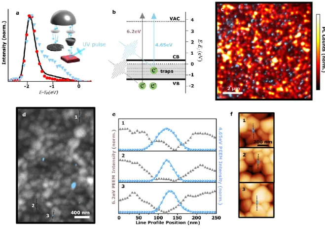
Figure 1. Photoemission electron microscopy revealing the spatial distribution of trap sites leading to non-radiative power losses in (Cs0.05FA0.78MA0.17)Pb(I0.83Br0.17)3 films. a) Spatially averaged photoemission spectra from a ~10 µm x 10 µm scan area (solid black line), and spatially resolved spectra from (blue triangles) and away from (red circles) a trap site in a (Cs0.05FA0.78MA0.17)Pb(I0.83Br0.17)3 thin film sample. Inset: Schematic of PEEM setup for imaging photoelectrons (blue spheres) emitted by the UV laser pulse (violet beam). Collected photoelectrons are imaged and magnified with electromagnetic lenses (grey cone and ovals) and can be energy filtered (silver hemisphere) before forming the final image. b) Energy- level diagram of the perovskite sample referenced to the Fermi level at 0 eV. Arrows represent transitions between states in the valence band (VB), conduction band (CB), trap states, and vacuum (VAC) for the UV laser pulses (4.65 eV and 6.2 eV photons, blue and grey arrows, respectively). The CB position is estimated from the band gap of the sample (~1.62 eV, see Extended Data Figure 1) relative to the band edge measured from panel a. c) Anti-correlation between nanoscale trap sites mapped by PEEM (blue) and local PL intensity. d) PEEM image from 4.65 eV pulses showing the location of nanoscale trap clusters (blue) overlaid on the 6.2 eV pulse PEEM image from the entire film, generated by photoemission from the valence band, showing the grain morphology (grey). e) Line profile of the intensity from the 4.65 eV pulse (blue) against the intensity from the 6.2eV pulse (grey). Numbering corresponds to regions of interest in panel (d). f) The same regions of interest as in d) and e) with PEEM maps from the 4.65eV probe overlaid on atomic force microscope (AFM) images.
To understand the spatial distribution of these occupied sub-gap trap states, we utilize the capability of our setup to spatially resolve photoemitted electrons. For this, we employ 4.65-eV UV pulses, which provide enough energy to overcome the work function (~3.9 eV) but not enough to photoemit electrons from the valence states, as illustrated by the blue arrow in Figure 1b. This allows us to selectively image the sub-gap states without needing to energy-resolve the photoelectrons. These photoemitted electrons are imaged in the microscope by electromagnetic lenses (inset of Figure 1a) to achieve a spatial resolution of 20 nm. Strikingly, as shown in the blue regions representing the PEEM intensity from sub-gap trap states in Figure 1c, we observe many isolated nanoscale trap sites on the sample, ranging in size from a few tens to a few hundreds of nanometers (see Extended Data Figure 5 for distributions). Spatially resolved photoemission spectra from these sites show a large density of sub-gap states (blue triangles, Figure 1a), but in spectra taken at regions away from these sites, the sub-gap states are notably absent (red circles, Figure 1a). We observe the same behavior from energy-resolved images using the 6.2-eV pulses (Extended Data Figure 6).
In Figure 1c, we show a confocal photoluminescence (PL) map of a region of the sample, highlighting the substantial spatial heterogeneity in the luminescence intensity, and overlay this on a PEEM image of the trap sites at the same location. We find a strong anti-correlation between the spatial location of these trap sites (i.e. PEEM intensity) and local PL intensity: regions of high PL intensity have very few trap sites, while regions with a high density of trap sites correspond to low PL intensity. A pixel-by-pixel plot of PL against PEEM intensity in Extended Data Figure 7 further elucidates the role played by the trap sites in contributing to non-radiative losses. The surface traps we observe here in PEEM have a significant impact on the observed PL variation
because even photo-excited carriers generated further into the bulk can diffuse much of the ~500 nm thickness of the film to the surface18. Bulk traps may additionally influence the PL, however these are likely of lower density. We also note that we do not observe any strong sub-band-gap absorption in our films (Extended Data Figure 1). Furthermore, Kelvin Probe Force Microscopy (KPFM) measurements overlaid on PEEM trap images reveal that the trap-rich local clusters observed in PEEM have a lower contact potential difference (CPD) with respect to the surrounding regions; a linear relationship between the CPD and the PEEM trap intensity allows us to use PEEM and KPFM measurements together as independent spatial indicators of the local trap distribution (Extended Data Figure 7). These results reveal that micron-scale dark regions in PL contain discrete, nanoscale trap clusters, rather than one single, uniformly defective region. The strong relationship between these trap states and the PL and CPD properties demonstrate the substantial impact of these trap states on optoelectronic performance.
In Figure 1d, we overlay these nanoscale trap sites (blue, 4.65-eV pulses) on the grain morphology of the film ascertained from valence band photoemission (grey, 6.2-eV pulse), which shows morphological grain boundaries at sites where the photoemission intensity is lowered.
Importantly, this overlay reveals that these nanoscale trap sites are located primarily at the junction between morphological grains: line profiles of PEEM intensity from the traps (blue) and morphological grain structure (grey) in Figure 1e show that the trap sites occur at specific grain boundaries. Complementary atomic force microscopy (AFM) images on the same scan regions and PEEM sites show that these sites are indeed morphological grains (Figure 1f).
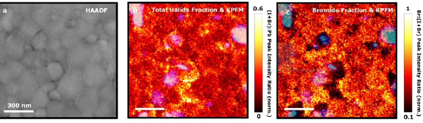
Figure 2. Probing the composition of grains associated with nanoscale trap clusters in (Cs0.05FA0.78MA0.17)Pb(I0.83Br0.17)3 thin films. a) High angle annular dark-field scanning transmission electron microscopy (HAADF-STEM) image of a region of interest revealing morphological grains. b) Ratio of total halide intensity counts relative to Pb: (I(I-Lα) + I(Br-Kα))/I(Pb-Lα), ascertained from STEM- EDX measurements. Some grains, and their grain boundaries, are particularly halide-rich. c) Fraction of bromide intensity counts out of total halide counts (I(Br-Kα)/(I(I-Lα) + I(Br-Kα))). The same distinct grains that were rich in halide are bromide-poor, while the rest of the region of interest (bulk, parent material) shows a homogenous distribution of Br. The compositional data in both b and c is normalized to 0 and 1 by subtracting the minimum value and scaling with the maximum value from the respective peak intensity ratio map. The trap states, indicated by KPFM measurements (blue), are overlaid on b and c and appear at the junction between the stoichiometrically ‘inhomogenous’ grains and the bulk parent material.
Local Structural and Compositional Properties at Defective Junctions
To probe how the nanoscale trap clusters, identified by PEEM and KPFM, relate to composition, we performed high-angle annular dark-field scanning transmission electron microscopy (HAADF-STEM), energy dispersive X-ray spectroscopy (STEM-EDX), and KPFM measurements on the same scan area of a (Cs0.05FA0.78MA0.17)Pb(I0.83Br0.17)3 sample. We show in Figure 2a a HAADF-STEM image, which shows morphological grain structure within the correlated region of the film. In Figure 2b, we show the normalised total halide-to-lead peak intensity ratio, (I(I-Lα) + I(Br-Kα))/I(Pb-Lα), obtained from STEM-EDX maps with a spatial resolution of ~10 nm. This image reveals that some distinct morphological grains contain an excess of halide relative to the rest of the region of interest, which is particularly exaggerated at the grain boundaries. We show in Figure 2c that these same morphological grains are also poor in bromide
(with respect to the surrounding material), ascertained from the normalised bromide fraction of peak intensity out of total halide counts, (I(Br-Kα) / (I(I-Lα) + I(Br-Kα))).This is consistent with these grains appearing brighter in the HAADF-STEM image (Figure 2a) because there are fewer light atoms (Br) and more heavy atoms (I) in these grains. The observed relative variations in halide content is not related to variations in the Pb content across the scanned region (Extended Data Figure 8). When we overlay the trap regions determined from KPFM measurements (blue regions) on the compositional intensity maps in Figure 2b and c, we find that the nanoscale trap clusters are almost exclusively associated with interfaces between these compositionally inhomogeneous morphological grains and the more homogeneous surrounding material. We refer to these sites herein as stoichiometrically “inhomogeneous grains” and the surrounding film as
“bulk parent material”. These results reveal that the majority of trap states appear at heterojunctions between these sites.
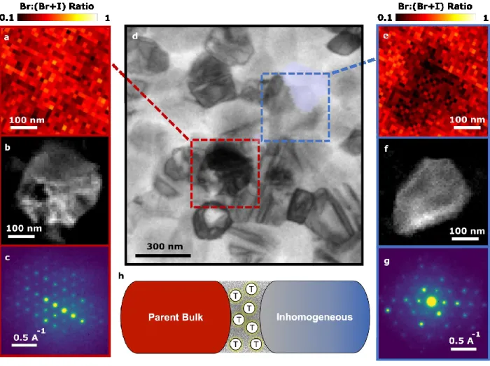
To better understand the local crystallography of these inhomogeneous grains and their relationship with trap clusters at grain boundaries, we correlate PEEM measurements with low- dose scanning electron diffraction (SED) microscopy and STEM-EDX measurements. To avoid beam-induced damage under electron radiation whilst maintaining a spatial resolution of ~4 nm, our SED experiments were performed with a local electron dose of ~6 e/Å2 (see Methods for experimental parameters to calculate dose), which is substantially lower than reported dose limits for halide perovskites in crystallography studies of ~100 e/Å2.19 We show a virtual bright-field (VBF) image of a region of a (Cs0.05FA0.78MA0.17)Pb(I0.83Br0.17)3 sample in Figure 3d, which we obtain by integrating the SED intensity around the direct beam as a function of probe position, and overlay on this image the PEEM measurement from the same scan area showing the location of the traps (blue). In Figure 3a, we show a STEM-EDX map of the selected area from the bulk parent material
in Figure 3d that is not associated with a trap cluster and has a uniform halide composition. Within this region, we identify a pristine grain (Figure 3b) from the parent material by performing a non- negative matrix factorization (NMF) analysis of the SED data. The grain revealed by NMF has the mean diffraction pattern shown in Figure 3c and can be indexed to near the (111) zone axis of cubic FAPb(I0.83Br0.17)3 (see Extended Data Figure 8 for indexation). We observe a similar cubic structure across other regions of the sample with homogeneous composition. A representative compositionally inhomogeneous grain (blue box in Figure 3d) is shown by the normalized halide intensity ratio from the STEM-EDX map (Figure 3e) and corresponds to a grain identified by NMF (Figure 3f). This grain is directly associated with the nanoscale trap cluster at its interface with an adjacent pristine grain (blue PEEM spot visualized in Figure 3d overlay). The mean diffraction pattern associated with the inhomogeneous grain is shown in Figure 3g and is structurally distinct from the pristine material. We note that this structure cannot be directly indexed to a cubic FAPb(I0.83Br0.17)3 or other known perovskite or PbI2 model (see Methods for further discussion).
Figure 3. High-resolution diffraction and compositional properties of nanoscale trap-rich heterojunctions in (Cs0.05FA0.78MA0.17)Pb(I0.83Br0.17)3 films. A virtual bright field image shown in d is extracted from scanning electron diffraction (SED) measurements and overlaid on a PEEM map showing the deep trap states (blue) on the same scan region. A pristine (red box) region and inhomogenous (blue box) region are subsequently analysed. a) (I(Br-Kα) / (I(I-Lα) + I(Br-Kα))) ratio extracted from a STEM- EDX map of the pristine (red box) parent region away from a trap site showing a homogeneous halide ratio.
b) Image of a pristine grain extracted from the SED data from the red region of interest in (d). c) Mean diffraction pattern of the compositionally homogenous grain in (a) and (b), revealing a cubic crystal structure corresponding to the nominal pristine composition. (e) (I(Br-Kα) / (I(I-Lα) + I(Br-Kα))) ratio extracted from a STEM-EDX map of the blue region of interest in (d) revealing the presence of an inhomogenous grain. (f) Image of a grain extracted from the SED data from the blue region of interest in d.
(g) Mean diffraction pattern of an inhomogenous grain from (e) and (f), which cannot be directly indexed to a cubic FAPb(I0.83Br0.17)3 model.(h) Schematic showing that the traps accumulate at the interface between compositionally and structurally homogeneous cubic parent regions and the inhomogenous, distorted regions. The compositional data in both a and e is normalized to between 0 and 1 by subtracting the minimum value and scaling with the maximum value from the respective peak intensity ratio map.
Ultra-fast Hole Trapping at Nanoscale Trap Clusters
Having imaged localized nanoscale trap sites on the film surface and identified their structural and compositional origins, we now study the specific influence of these traps on photo- excited charge carrier recombination by using time-resolved PEEM (TR-PEEM) measurements to visualize the ultrafast trapping dynamics10,11. We first photoexcite the sample with a near-infrared, ultrafast pump pulse (1.55 eV) and subsequently image the sample using a time-delayed ultrafast UV probe pulse (Figure 4b). Here, we study the dynamics of an iodide-only analogue sample (Cs0.05FA0.78MA0.17)PbI3, which has a band gap of ~1.54 eV (Extended Data Figure 1), thus enabling us to have a resonant excitation condition; we note that we see similar trap characteristics as in the bromide-containing samples (Extended Data Figures 5, 6) and also see similar kinetics (Extended Data Figure 9). We use the 4.65-eV UV probe pulses to image electrons exclusively from occupied trap states (cf. blue transition in Figure 1b). Thereby, we are able to construct movies of the photocarrier trapping dynamics from sequences of images at varying pump-probe time delays.
Figure 4. Nanoscale photo-excited carrier trapping dynamics in (Cs0.05FA0.78MA0.17)PbI3 samples. a) Overlaid PL and PEEM images from a (Cs0.05FA0.78MA0.17)PbI3 thin film. b) Schematic of the TR-PEEM setup for time-resolved imaging of photoelectrons. A pump pulse (1.55 eV, red beam) first excites the sample. Then, a time delayed (Δt) UV probe pulse (4.65 eV, violet) measures the pump-induced change in electron population by photoemitting electrons (blue spheres) into the PEEM microscope. c) Measured TR- PEEM signal as a function of delay time (I(t)) plotted as the percent change (100 x (I(t) – I0)/I0) in PEEM intensity against the initial unphotoexcited PEEM signal I0 before arrival of the pump pulse (negative time delay). The signal is extracted from all the trap spots within the ~10 µm field of view. The grey line is a double exponential fit to the data with time constants τ1 = 7 ± 2 ps and τ2 = 79 ± 3 ps and amplitudes A1 =
2.4 ± 0.4 and A2 = 10.5 ± 0.3. Inset shows a simplified energy diagram, where the pump photons (red arrow) excite electrons (blue circles) from the valence band (VB) to the conduction band (CB). The trap states occupied with electrons can then trap holes (hollow blue circles), where an electron moves from the trap state to the valence band (green arrow). d, e) TR-PEEM images from the marked areas in (a) showing the change in photoemission intensity (I(t) – I0) with time delay after excitation. f) PEEM image of several traps (same location as panel d), with two trap sites and a trap-free region marked (blue, green, and red rectangles, respectively). g) Extracted TR-PEEM signal from the nanoscale spots marked in (f). The two marked trap sites (blue circles and green triangles) show the hole trapping dynamics, while the trap-free area (red squares) shows a negligible signal change. h) Fitted time constants τ2 for different trap site intensities I0. Error bars denote the standard error from the exponential fitting for each intensity bin, where the number of traps measured for each bin is shown by the histogram in Extended Data Figure 12b. The dashed grey line represents the mean (85 ps) of the data.
Upon photoexcitation, we first observe that the photoemission intensity measured from the trap states decreases (Figure 4c), implying a decrease in electron occupation after photoexcitation, i.e.
photo-hole trapping, as illustrated in the inset of Figure 4c. We note that the absence of a sharp decrease in the photoemission signal at zero time delay indicates that there is no significant direct excitation of electrons out of the trap states by the pump. We then compare the TR-PEEM movies between low and high PL regions of the sample (Figure 4a). In regions of low PL efficiency (yellow box in Figure 4a), we see complex spatio-temporal dynamics with photo-excited holes being trapped at several discrete sites (Figure 4d and Extended Data Video 1). In striking contrast, regions of high PL efficiency (green box in Figure 4a) show little to no photo-excited hole trapping (Figure 4e and Extended Data Video 2). From the time-resolved images (Figure 4d and Extended Data Video 1), we extract spatially resolved dynamics from selected trap clusters. For local spots of substantial trap density (blue and green rectangles, Figure 4f) we measure the photo-excited hole trapping signal (Figure 4g blue circles and green triangles, respectively), while in regions of low trap density (red rectangle, Figure 4f) we see no change in PEEM intensity (Figure 4g red squares). We observe this trend across different samples, locations, and for repeated measurements (see Extended Data Figure 10 for additional TR-PEEM images). Previous reports on MAPbI3 films
have identified electron trapping as the dominant non-radiative pathway, with hole traps, if present, playing a more minor role20,21. By contrast, we show in these mixed cation systems that hole traps significantly influence charge carrier dynamics on a sub-nanosecond timescale and directly correlate with the primary sites of non-radiative losses. We note that our measurements cannot exclude the additional possibility of electron traps in these mixed cation films, particularly if the electron capture happens on a longer timescale.
We develop further insight into the hole trapping dynamics via a quantitative analysis of the process at different sites. First, a double exponential fit to the spatially averaged data in Figure 4c (see Methods for details and alternative equivalent approaches) is used to extract the trapping time, where the slower τ2 time constant of 81 ± 21 ps is found to be the main contribution to the signal amplitude. We then extract the τ2 time constant as a function of the trap density (proportional to the photoemission intensity I0)from all the individual trap sites within the PEEM image using a binning procedure (see Methods). Importantly, we find that this dominant time component is independent of trap density (Figure 4 h), revealing that the initial trapping kinetics are not limited by the trap density of a site. Rather, we attribute this time scale of ~80 ps to the time it takes for photo-excited holes to reach the trap sites through diffusion. By assuming a diffusion coefficient D of ~1 cm2s-1 (for intra-grain diffusion22), this time scale would correspond to a trapping length (𝐿 = √𝐷𝜏 ) of approximately 90 nm, which is comparable to half of the mean distance between neighbouring trap sites for the samples (Extended Data Figure 5). Such a diffusion-limited trapping process is consistent with previous diffraction-limited optical measurements22. Due to the resonant photoexcitation conditions in the time-resolved measurements reported here, we expect that thermal effects such as carrier heating or phonon bottlenecks23 do not influence the dynamics we see, and are not responsible for the removal of electrons from the occupied traps. However, we
note that other processes, such as carrier-carrier and carrier-phonon interactions or phonon-assisted trapping and de-trapping processes24, may also play a role. Under our experimental conditions, we are not able to observe a transient signal related to free carriers in the conduction band (see Methods for discussion), and therefore future work will require complementary measurements of carrier kinetics for a complete understanding of all carrier recombination processes.
Discussion
Our combined results show that deep photo-excited hole traps form at the interfaces between pristine grains with expected halide ratios and cubic structure, and grains that are compositionally inhomogeneous with a distorted structure. Any heterogeneity in the local A-site cation distribution25 could further exacerbate these defective junctions. The interface between the pristine material and compositionally inhomogeneous regions results in a distribution of electronic states above the valence band, which can be explained by a defect segregation that varies across the interface, for example, driven by the strain between the inhomogeneous phase and the parent material (see Figure 3h). In particular, for iodine interstitial defects, which form charge transition levels deep in the band gap that could trap holes26–28, a higher concentration will be formed at the grain boundaries owing to the local excess of halide at these locations29. Further work will be required to explain why deep trap states form at only one localised interface between the compositionally inhomogeneous grains and the bulk pristine material, though it may relate to grain orientation, or a specific strained contact point at which defects pool.
Our conclusions have profound implications for our understanding of the nanoscale behavior of halide perovskites. We have shown that trap sites associated with non-radiative recombination - which influences charge-carrier lifetime, solar cell open-circuit voltage and ultimately limits device performance30 - appear in nanoscale clusters. While there is consensus in the community
that device performance improves with better homogenization of the halide content in mixed- halide systems31, the underpinning mechanism of this improvement has, until now, remained unclear. The fact that these surface traps almost exclusively form at these local junctions provides rational strategies for the removal of these states, while also suggesting the tantalizing prospect that further traps may not form at other locations. Thus, passivation and growth strategies that target the removal of these inhomogeneous and distorted grains will be critical for the elimination of performance losses and instabilities. The localized but sparsely distributed nature of these trap clusters may also give insight into the apparent defect tolerance of these materials. Finally, the correlated multimodal framework presented here has applications extending far beyond halide perovskites as the ability to locate and identify the structural and compositional origins of deep trap states will be applicable to a wide range of beam-sensitive semiconductor material families including bulk inorganic and 2D materials.
Methods
Perovskite preparation
All perovskite films were prepared in Cambridge in a N2-filled glove box.
(Cs0.05FA0.78MA0.17)Pb(I0.83Br0.17)3 perovskite thin films were prepared from solutions containing FAI (1 M), MABr (0.2 M) PbI2 (1.1 M), PbBr2 (0.22 M) dissolved in anhydrous DMF:DMSO 4:1 (v:v). CsI dissolved in DMSO (1.5 M) was then added to the precursor solution.
(Cs0.05FA0.78MA0.17)PbI3 thin films were prepared from precursor solutions containing FAI (1 M), PbI2 (1.32 M), and MAI (0.2 M) in anhydrous DMF:DMSO 4:1 (v:v). CsI dissolved in DMSO (1.5 M) was then added to the precursor solution. For the PEEM, PL and PDS data presented in Figure 1, 4, and Extended Data Figures 1, 3, 5, 6, 7, 9, 10, 11 and 12 the precursor solution was spin coated onto ITO substrates (ranging in size from 0.8cm x 0.8cm to 1cm x 1cm) in two steps at 2000 and 4000 rpm for 10 and 35 seconds, respectively, with 100 µL of chlorobenzene added 30 s before the end of the second step. The films were then annealed at 100 C for 1 hr. In all our samples fabricated in this manner, we obtained film thicknesses of ~500 nm. For the SED/PEEM and STEM-EDX/KPFM correlation data presented in Figure 2, 3 and Extended Data Figure 8 the perovskite solution was diluted in anhydrous DMF:DMSO 4:1 (v:v) (2:1 ratio of dilutant to precursor solution) and then spin coated on Agar Scientific SiN TEM grids (3mm diameter) (Product number: AGS171-2) in two steps at 2000 and 6000rpm for 10 and 35 secs respectively, with 20 l of chlorobenzene added 30s before the end of the second step. In all our samples fabricated in this manner, we obtained film thicknesses of ~200 nm required for electron transparency. Fiducial Au markers were deposited by spin-coating a suspension of Au nanoparticles in chlorobenzene at 1000 rpm for 20 s, which were used for spatial alignment of the sample between different measurement techniques. These uniquely and randomly shaped markers
are small (few micrometers in size), dilute in distribution (few markers per mm2), and measurements were made several microns away from the marker itself32. As a result, and as confirmed by control experiments, these Au markers do not impact our measurements8. Samples for PEEM measurements were then sealed in air-tight packaging and sent to OIST, where they were stored and re-opened in a N2 glovebox. Samples were loaded onto the PEEM sample holder inside the N2 glovebox and transferred to the UHV system through a vacuum/N2 compatible suitcase. Devices used to obtain the data presented in Extended Data Figure 2 were prepared as follows. ITO substrates were cleaned with Hellmanex III Soap, DI water, Acetone and Isopropanol with sonication for 30 minutes each. UV ozone was employed to clean the substrate and improve the surface wetting for 15 mins before the hole transporting layer deposition. For the poly(triaryl amine) (PTAA) layer, 5 mg/ml PTAA (MW: 19,000) in anhydrous toluene was spun on to the ITO substrate at 4000 rpm for 30 second. The film was then annealed on a hotplate at 100°C for 10 mins. Due to the hydrophobic nature of PTAA, we spun a poly[(9,9-bis(30-((N,N-dimethyl)-N- ethylammonium)-propyl)-2,7-fluorene)-alt-2,7-(9,9-dioctylfluorene)] dibromide (PFN-P2) solution (1-Material) (0.5 mg/ml) to improve the wetting and passivate the interfaces33. To fabricate the perovskite film, the (Cs0.05FA0.78MA0.17)Pb(I0.83Br0.17)3 perovskite precursor (prepared as above) was spin coated on the substrate in a two-step process: 1000 rpm for 10s and 6000 rpm for 20s. 100 µl chlorobenzene was introduced in the middle of the film 5s before the end of the second step and the perovskite layer was then annealed at 100°C for 1h. The electron transporting layer deposition was completed by spinning [6,6]-Phenyl-C61-butyric acid methyl ester (PCBM) (20 mg/ml, Merck) on top of perovskite film at 1200 rpm for 30 sec. The bathocuproine (BCP) solution (0.5 mg/ml, Alfa) was dynamically spin coated on the PCBM layer
to form a buffer layer. The back contact electrode, Ag, was thermally deposited at a rate of 0.1 Å/s for the first 2 nm and then a rate of 1 Å/s thereafter to achieve a thickness of 100 nm.
Device characterisation
For current density-voltage curve measurement, a source meter (Keithley 2400) was used to record the parameter. A standard Silicon reference diode (no filter) was used to calibrate the light intensity to one sun AM1.5 G of 100mW/cm2. The mismatch factor of 1.13 for a band gap of 1.6 eV was accounted for during calibration. A 450 W Xenon lamp equipped with Abet solar simulator was used as a light source. The scan of J-V curve was from -0.1 to 1.2 V (forward scan) and 1.2 to -0.1 V (reverse scan) with a scan rate of 100 mV/s and a step size of 0.02 V. A mask with an aperture size of 8.3 mm2 was used. All device measurements were conducted in air without any encapsulation, pre-bias or light-soaking conditions.
TR-PEEM setup
The source laser used for PEEM and TR-PEEM imaging was a 4 MHz, 650 nJ Ti:Sapphire oscillator (FemtoLasers XL:650) delivering 45 fs pulses at 800 nm. The laser is split into two paths; one path is used for generating the UV pulses for PEEM imaging, while the other is used for the pump pulses for excitation in time-resolved measurements. The 4.65 eV UV pulses are generated as the third harmonic of the 1.55 eV (800 nm) fundamental via sum frequency generation of the fundamental and the 3.10 eV (400 nm) second harmonic. The 6.2 eV UV pulses are then generated via sum frequency generation of the 4.65 eV (266 nm) third harmonic and the 1.55 eV (800 nm) fundamental34. The pump is sent to a variable 200 mm delay stage which controls the time delay between pump and probe pulse arrival at the sample. The probe and pump lasers are focused into the ultra-high vacuum chamber of the PEEM instrument (SPELEEM, Elmitec GmbH)
where they are incident at a grazing angle of about 17° on the sample. The pump spot size was approximately 70 µm FWHM (short axis of ellipse) at the sample while the probe was loosely focused to about 250 µm FWHM to provide more uniform imaging. The UV pulses were set to p- polarization while pump pulses were s-polarized. Typical UV pulse fluences used were approximately <100 nJ/cm2 for the 3rd harmonic (4.65 eV) and <10 nJ/cm2 for the 4th harmonic (6.2 eV). UV pulse fluences were chosen as a balance between PEEM intensity and space charge effects35; generally, the UV fluence was reduced to a level where no or minimal broadening of the photoemission spectrum could be observed. The 1.55 eV pump pulse fluence used for time- resolved measurements was about 20 µJ/cm2 for (Cs0.05FA0.78MA0.17)PbI3 thin film samples. The overall temporal resolution of our experiment was estimated to be about 300 fs from the measured pump-probe temporal overlap in TR-PEEM10,11.
PEEM Image acquisition and processing
Measurements were performed at room temperature in the UHV chamber of the PEEM instrument, with a base pressure of 10-10 torr or better. TR-PEEM images and PEEM images of the trap sites were taken with 3rd harmonic (4.65 eV) pulses, a field of view (FOV) of 10 µm, and no contrast aperture. Energy resolved images and photoemission spectra were taken using 4th harmonic (6.2 eV) pulses, no contrast aperture, and with the hemispherical energy analyzer slit set to 250 meV energy resolution. The Fermi level of the system was referenced to the high kinetic energy edge of nearby gold markers deposited on the sample.
Higher resolution PEEM images of the traps and film morphology were taken with a FOV of 7.5 µm and a 100 µm contrast aperture. PEEM images of the surface morphology were taken with 6.2 eV pulses, the energy analyzer set to 250 meV energy resolution, and integrated at the valence band peak energy (centered roughly at E-EF = -2 eV). With the contrast aperture inserted, we could
achieve a spatial resolution in PEEM of about 20 nm, as estimated from the line profiles in Figure 1 e using an 84/16% criteria. Images taken without the contrast aperture inserted had a resolution as good as about 40 nm.
All PEEM images were corrected using a flat field method to remove the non-uniformity in the instrument main channel plate and phosphorescent screen. For time-resolved measurements, typical image conditions for a single frame (single pump-probe delay step) were 4 s exposure with two averages. In order to reduce artifacts from sample drift and laser intensity fluctuations, TR- PEEM experiments were taken with multiple repeat scans (5 repeats for the data shown in figure 4). Any sample drift in position or slow intensity variations over the repeated scans are then corrected during analysis before averaging the scans together. For extracted TR-PEEM intensity curves, intensity fluctuations of the laser are reduced at each delay step by normalizing the TR- PEEM signal to the photoemission intensity of the gold markers within the same image used as position references.
Displayed TR-PEEM images are averaged with a rolling average window of 5 frames between delay steps to smooth image-to-image noise. To view the changes due to pump excitation, the TR- PEEM images shown have been subtracted by the average of the unphotoexcited PEEM images taken at a negative pump-probe delay (i.e., probe arriving before pump excitation) during the measurement sequence.
For energy resolved images, the spatial variation of the measured kinetic energy due to the hemispherical analyzer dispersion was corrected using a uniform area (e.g. Au marker) as a reference. Exposure times for energy resolved images (for photoemission spectroscopy) with the 4th harmonic were 20 s with four averages per image for the data shown in Figure 1 a. The background noise of the instrument was removed by subtracting images at lower kinetic energy
where there is no photoemission intensity. Spatially resolved photoemission spectra are extracted from selected areas of the sequence of images at different kinetic energies (see Extended Data Figure 6).
Analysis of Trapping Dynamics
As stated in the main text, we did not observe any TR-PEEM signals related to free carriers in our measurements here. Free carriers in the conduction band would have resulted in a sharp transient (pulse width limited) increase in the measured TR-PEEM signal, which was not observed in these measurements, as well as in attempts at spectroscopic (energy resolved) TR-PEEM measurements.
There are several reasons why the signal from free carriers in the conduction band could not be observed, though at this time it is unclear which is the exact cause. Three likely issues are: having an unfavorable transition probability for the probe photon, momentum conservation in the photoemission processes, and a low density of states at the band edge. For the first issue, it is possible that there is no allowed optical transition between the conduction band minimum and a state above the vacuum level at the energy of our probe photon, making the signal too weak to detect. This transition must conserve energy, momentum and spin, which is a general requirement of photoemission spectroscopy36,37. The second issue follows from this requirement, where for a FA-based perovskite at room temperature (cubic phase), the band gap was calculated to be at the high-momentum R point in the Brillouin zone 38.To maintain momentum conservation, this would require an additional photon energy of about 11 eV (assuming a cubic lattice with a ~ 6.3 Å) on top of the energy needed to overcome the work function and binding energy. Since we only have probe energies of 4.65 and 6.2 eV, we cannot directly probe such a high momentum point in the Brillouin zone, and this would prevent us from observing free carriers in the conduction or valence bands. The third issue could be due to the low density of states (DOS) at the band gap which has
been discussed previously in the literature39. This could result in time-resolved signals being very small and difficult to detect above the background photoemission signal from other states.
We also note that we have checked for effects due to surface band bending. Measurements comparing surface photovoltage (SPV) shifts of the photoemission spectrum (between negative and positive pump-probe time delays) under the same experimental conditions have shown only small shifts of a few tens of milli-electronvolts, which is below the energy resolution of the analyzer. Therefore, band bending effects here are likely small and should not affect either the static or time resolved photoemission measurements discussed here.
Now, we discuss in more detail the analysis used for the measured hole trapping dynamics. Unless stated otherwise, TR-PEEM curves are fit with a double exponential equation:
𝑦(𝑡) = 𝐴1(𝑒−
𝑡
𝜏1− 1) + 𝐴2(𝑒−
𝑡 𝜏2− 1)
Where A1 and A2 are amplitudes, and τ1 and τ2 are the fast and slow time constants, respectively.
Due to its low amplitude the τ1 time constant is not always well resolved in these measurements.
We note that while we use a bi-exponential function for a better fit, we still observe the same lack of dependence of the trapping time for both single exponential and stretched exponential fits (see Extended Data Figure 11). Across several spatially averaged measurements on (Cs0.05FA0.78MA0.17)PbI3 samples, the mean amplitudes and time constants are A1 = 4.0 ± 2.0, and A2 = 12 ± 5, τ1 = 9 ± 4 ps, and τ2 = 81 ± 21 ps, where the error is the standard deviation across 6 different measurements.
Next, we describe the analysis used to compare TR-PEEM signals between different trap sites intensities. Based on the monomolecular Shockley-Read-Hall (SRH) trapping formalism, the trapping dynamics should depend on the trap density and thus the initial photoemission signal
I0.40,41 To compare across all the trap sites within the PEEM image, we then implement a binning procedure to compare the TR-PEEM signal between groups of trap sites, which is outlined below.
First, any artifacts or unwanted signals, such as the edge of the image or the gold position markers, are masked from the image (Extended Data Figure 12 a). Then, the image is processed using an intensity threshold and a connectivity algorithm is used to identify all the trap sites within the image and sort them based on their intensity (Extended Data Figure 12 b). The TR-PEEM signal is then extracted separately for each binned intensity level and then fit with a double exponential decay. The TR-PEEM signals (colored dots) and corresponding fits (grey lines) for 4 of the bins are shown in extended data figure 12c, and are offset for clarity. The resulting time constants and amplitudes as a function of the unphotoexcited PEEM intensity are shown in Extended Data Figures 12 d and e, respectively, with the error bars representing the fitting error for each intensity bin. We note that due to its low amplitude, the τ1 time constant is not reliably fit for many bins.
Any empty bins and bins with no signal (i.e. the fit routine fails to converge) are excluded from extended data figure 12 d and e. We also show the fitting results using single exponential and stretched exponential functions in Extended Data Figure 11. From this analysis, we find that the trapping time constants measured (Extended Data Figure 12 d) are independent of the trap intensity, indicating that the trapping kinetic is not following the expected SRH behavior and therefore must be limited by a slower mechanism.
Photoluminescence measurements
Photoluminescence maps on (Cs0.05FA0.78MA0.17)Pb(I0.83Br0.17)3 for correlation with PEEM image (Figure 1c and Extended Data Figure 7e) was acquired on a Leica TCS SP8 STED3X confocal microscope. The excitation source was a CW 442 nm diode laser with an intensity of about 2 µW (~ 1.7 kW/cm2, assuming a diffraction limited probe), focused through an oil objective (100x
magnification, 1.4 NA). PL was collected across a 15 µm x 15 µm region (15 nm step, 200 Hz scan speed). Maps were acquired after regions of interest had been identified and measured in PEEM, using gold particles as fiducial markers.
Photoluminescence maps on (Cs0.05FA0.78MA0.17)Pb(I0.83Br0.17)3 deposited on a SiN x-ray window and perovskite devices (Extended Data Figure 2) were acquired using a Picoquant MicroTime 200 Confocal Microscope. The excitation source was a pulsed 404 nm laser (2 MHz repetition rate), focussed through an objective lens (100x magnification, 0.9 NA) with an average power of 1.3 nW (~ 550 mW/cm2, with a measured probe size of ~550 nm). PL was collected across a 15 µm x 15 µm region (59 nm pixel size, 300 µs dwell time).
Photoluminescence maps on (Cs0.05FA0.78MA0.17)PbI3 films were performed in a confocal microscope configuration (Nanofinder 30) using a 532 nm excitation laser with an intensity of 50 nW ( ~ 9.7 W/cm2 assuming a diffraction limited probe) focused through a 0.8 NA (100x) objective.
PL maps were acquired by scanning the laser spot with a galvanic mirror in 100 nm steps.
Spectroscopic measurements (PL in Extended Data Figure 1) on both film compositions were performed in the same setup with 5 nW intensity (~ 970 mW/cm2) and averaged over a few micrometer scan area. For generating the overlay in figure 4a (and Extended Data Figure 10), the PEEM and PL images are overlaid and aligned using the gold marker as a position reference.
All PL measurements correlated with PEEM were performed in air after PEEM and TR-PEEM experiments and were aligned to the same sample location via fiducial gold markers placed during film preparation.
Spectrally-resolved photoluminescence images (Extended Data Figure 3d) and the accompanying spectra (Extended Data Figure 3c) were acquired with an IMA wide-field hyperspectral
microscope (Photon Etc). Continuous wave excitation was provided by 405 nm laser with intensity below 3 suns (250 mW/cm2), through a 20x objective lens. Spatially averaged PL spectra were extracted from each image and local spectra (Extended Data Figure 3c inset) were extracted from the highlighted regions of “PEEM exposure” and “no PEEM exposure”. Optical reflectance images (Extended Data Figure 3b) were measured on the same setup using white light illumination.
Absorption measurements
Photothermal deflection spectroscopy measurements were acquired on a custom-built set-up by monitoring the deflection of a fixed wavelength (670 nm) laser probe beam after absorption of each monochromatic pump wavelength by a thin film immersed in an inert liquid FC-72 Fluorinert (3M)
Absorption measurements to determine quantitative changes in films after shipping and extreme PEEM exposure measurements (Extended Data Figure 3a) were performed with a Shimadzu UV- 3600 Plus with ISR-603 integrating sphere attachment. Measurements were carried out in transmittance configuration and referenced to an ITO/glass substrate.
SED Measurements
Scanning electron diffraction (SED) microscopy involves recording a two-dimensional electron diffraction pattern at every probe position as a focused electron beam is scanned across the sample. SED data was acquired on the JEOL ARM300CF E02 instrument at ePSIC, Diamond Light Source. The key capability offered by the E02 instrument at ePSIC is the Merlin/Medipix pixelated STEM detector for fast scanning electron diffraction. Utilising this highly sensitive detector and the following experimental parameters: accelerating voltage = 300 kV; nanobeam alignment (~1 mrad convergence angle); electron probe ~4 nm; probe current ~2 pA; scan dwell
time 1 ms; camera length 15 cm, we can achieve an electron dose per scan of ~6.25 eÅ-2 when approximating the beam shape as a circle with a diameter of 4nm. This accumulated dose is over an order of magnitude lower than the reported damage threshold for MAPbI3 (100 eÅ-2) 19,42. We note that the beam shape is in fact an Airy disk and calculating the electron dose with the circle approximation slightly over-estimates the accumulated electron dose. SED diffraction data was analysed in pyXem43. In the manuscript, we refer to virtual bright field (VBF) images. VBFs are reconstructed from SED data by plotting the intensity integrated around the direct beam as a function of probe position. The resulting image is formed exclusively by directly transmitted electrons.
Analysis of Diffraction Data
All diffraction patterns obtained from the bulk parent material can be indexed as a cubic FAPb(I0.83,Br0.17)3 crystal with a lattice parameter of ~6.30 Å. This is consistent with Vegard’s law for FAPbIxBr1-x and a random alloy over the predominantly cubic FA-rich sites in the (Cs0.05FA0.78MA0.17)Pb(I0.83Br0.17)3 composition. Any variations that would occur in diffraction patterns between the simple FAPb(I0.83,Br0.17)3 cubic model used for indexation here and the more complex (Cs0.05FA0.78MA0.17)Pb(I0.83Br0.17)3 structure that the samples are in fact composed of, are minor and beyond the reciprocal space resolution of our techniques. In SED, under these operating conditions, 1 pixel on the Merlin/Medipix pixelated STEM detector is ~ 0.014 A-1. Diffraction patterns are calibrated with an Au cross grating.
SED data was treated with principal component analysis (PCA) to denoise the data. PCA sorts the signal into orthogonal components (linear combinations of variables) in decreasing order of variance. The high-variance components constitute the data’s primary features while low- variance components represent noise. The number of high-variance components (primary features)
was estimated by plotting the explained variance of the dataset vs the component index (Extended Data Figure 10a,b) and detecting the point at which the scree plot becomes linear by utilising the knee finding technique of Satopaa et al.44. Non-negative matrix factorisation (Figure 3b,f) was then performed with the output-dimension specified by the PCA scree plot. For the homogeneous grain shown in figure 3b, an output dimension of 3 was used (Extended Data Figure 8d), while for the inhomogeneous grain shown in figure 3f, an output dimension of 5 was used (Extended Data Figure 8f)45.
For the inhomogeneous grain, the vector lengths marked in Extended Data Figure 8g of 0.898 A-1 and 1.116 A-1 (marked as 1 and 2 respectively in Extended Data Figure 8g) compare closely to theoretical lengths of the cubic (440) and (444) reflections in cubic FAPb(I0.83Br0.17)3, which are 0.902 A-1 and 1.099 A-1 respectively. In this respect, the component diffraction pattern from the compositionally inhomogeneous grain is similar to a (110) zone axis pattern from cubic FAPb(I0.83Br0.17)3 and may be consistently indexed as pseudo-cubic. However, crucially, the (100) and (110) type reflections are not detectable and the angle between the (200) and (220) planes (marked as θ in Extended Data Figure 8g) is 87.6º instead of the nominal 90º for the cubic parent material. Similarly the diffraction pattern is geometrically close to the 101 zone axis of PbI2 but the differences between experimental and theoretical measured diffraction vector lengths and angles are substantially larger than in the successfully indexed bulk parent material. It is difficult to construct an intuitive atomic model based on either of these starting points that adequately accounts for all diffraction measurements from the compositionally inhomogeneous grains; further work will be required to determine the local atomic structure unambiguously.
STEM/EDX Measurements
HAADF-STEM images and STEM-EDX spectrum images were acquired using an FEI Tecnai Osiris (S)TEM equipped with a high brightness Schottky X-FEG gun and a Bruker Super-X EDX system composed of four silicon drift detectors, each approximately 30 mm2 in area and placed symmetrically around the optic axis, achieving a total collection solid angle of ~0.9 sr. Spectrum images were recorded using a 70 μm C2 aperture at an accelerating voltage of 200 kV, a beam current of ~250 pA, a spatial sampling of 10 nm/pixel and a dwell time of 50 ms/pixel. All data was acquired with TEM Imaging Analysis (TIA) and analyzed with Hyperspy 46. STEM-EDX was performed last as it requires the highest probe current to generate meaningful data.
STEM-EDX Analysis
STEM-EDX data was analysed in the open source Python package Hyperspy 46. To improve the signal-to-noise ratio of the spectra, the energy axis was rebinned by four and the data was treated with principal component analysis (PCA) for denoising. Briefly, as above, PCA sorts the signal into orthogonal components (linear combinations of variables) in decreasing order of variance.
The high-variance components constitute the data’s primary features while low-variance components represent noise. By removing the noise components, PCA greatly increases signal-to- noise ratio while retaining almost all variance, thus preserving statistical significance47. Ratio maps were then constructed by dividing the appropriate peak intensity maps.
KPFM Measurements
KPFM was performed on a wafer-scale atomic force microscope (AFM), the Dimension Icon Large Sample Tip from Bruker. Here, all KPFM maps were 512 × 512 pixels acquired in frequency-modulated KPFM imaging mode at a typical scan rate between 0.3-0.4 Hz. For our
measurements we used Pt-Ir coated Si probes from Bruker, (model: SCM-PIT) which have an average resonant frequency = 75 kHz and spring constant = 2.8 N/m. All measurements were performed in the dark and in ambient atmospheric conditions. Perovskite samples deposited on both ITO and SiN substrates (Extended Data Figure 2) were KPFM mapped and variations in V of comparable magnitudes and spatial distributions are observed on both substrates. We note that the difference in CPD observed between the regions at a trap site, and away from a trap sites, is similar to the energy resolution of our PEEM setup (~150 – 200 meV).
SEM measurements
SEM imaging was performed at 5 kV electron energy with a LEO Gemini 1530VP FEG-SEM.
AFM measurements
AFM measurements (Figure 1f) were obtained with a Bruker ICON3-OS1707 atomic force microscope in tapping mode.
XRD measurements
X-Ray Diffraction data was acquired at synchrotron beamline I14 of the Diamond Light Source utilizing a 20 keV monochromatic X-ray beam (λ = 0.619 nm). Diffraction data was recorded on an Excalibur 3M detector consisting of 3 Medipix 2048 x 512 pixel arrays. 2D detector images were calibrated with a CeO2 calibrant and radially integrated in The Data Analysis WorkbeNch (DAWN). The XRD data was averaged over a sample area of 30 x 30 µm2.
Exposure Controls
The issue of material stability and sensitivity to exposure is an important ongoing problem in HOIP studies and applications. Below, we show measurements, including absorption, emission, and
structural measurements on (Cs0.05FA0.78MA0.17)Pb(I0.83Br0.17)3 samples freshly made, after shipping, and after intense and long-term exposure to our PEEM experimental conditions, namely the UV laser probe and UHV. The PEEM exposure in these measurements was ~7 hrs long with
~100 nJ/cm2/pulse of UV light (total dose of ~10 kJ/cm2). This long term and intense exposure to PEEM conditions for the control measurements was necessary to stress the samples in an extreme way in order to begin seeing degradation effects. In contrast, the typical experimental conditions used in the manuscript were ~20 mins of sub-100 nJ/cm2/pulse of UV exposure (< 0.5 kJ/cm2 total dose for a single time resolved measurement) or ~1 hr of sub-10 nJ/cm2/pulse (< 0.3 kJ/cm2 total dose for spectroscopic PEEM measurements). As discussed below in more detail, the doses on the sample during our actual measurement conditions are over an order of magnitude lower and do not affect the results of our experiments.
Absorption: In Extended Data Figure 3a, we show the absorption of fresh films (black), after shipping (red), and after intense and long-term exposure to PEEM conditions (blue). We see no appreciable changes in the absorption edge.
Optical Reflectivity: In Extended Data Figure 3b, we show the optical reflectivity image of a sample, where part of the sample has been exposed to the intense and long-term PEEM experimental conditions (red dashed ellipse). There is no visible change in the sample surface after the exposure, in agreement with the optical absorption measurements.
Photoluminescence: In spectrally resolved measurements (Extended Data Figure 3c), we see that there is no appreciable change in the central wavelength or the emission width of the PL from fresh films (black), after shipping (red), and after exposure to the intense and long term PEEM conditions (blue). We do, however, see a ~30% decrease in PL intensity after the extended PEEM exposure (Extended Data Figure 3c inset). The ~30% reductions we observe after extensive
exposure are consistent with previous literature, where PL yield is known to decrease due to effects such as light induced ion migration under vacuum conditions28,48. Again, we note that for the reported experiments in the manuscript, the UV exposure is more than an order of magnitude smaller in dose and thus its effects are significantly smaller (< 1% as shown below).
PEEM Maps: During the intense and long-term PEEM exposure (UV + UHV) itself, we can monitor the PEEM image and the corresponding intensity of the trap sites over time. By comparing PEEM images taken before and after the intense PEEM exposure (Extended Data Figure 3e & f), we see that the spatial distribution of the traps is unchanged. We do find that there is a ~30-40%
increase in the intensity of the traps after the ~7 hr exposure to UV light (Extended Data Figure 3g). This corresponds well with the measured reduction in PL after the exposure. In fact, this PEEM measurement begins to provide a nanoscopic view into how changes in defect sites cause a decrease in radiative efficiency upon light exposure, thus presenting another important avenue for future research.
XRD Measurements under regular exposure: Lastly, we also discuss here control checks done under regular PEEM exposure conditions. First, we show XRD measurements averaged over a ~30 x 30 µm2 area (Extended Data Figure 4a) on freshly made samples (black curve) and on samples which were shipped and imaged in PEEM (blue curve). We observe no differences in the crystalline quality of the samples.
PEEM Measurements under regular exposure: We also show a set of repeated TR-PEEM pump- probe scans ((Cs0.05FA0.78MA0.17)Pb(I0.83Br0.17)3 sample, 1.55 eV pump, 4.65 eV probe), where we plot the real time during the measurement on the bottom x-axis (Extended Data Figure 4b). For the sequence of 5 repeated scans, by comparing the intensity of the negative time delay points at the start of each scan, we see that there is a small change of about ~4% (dashed gray lines) over
the total ~80 min measurement time. This rate of change matches our observation from the more extensive exposure (~30% in 7 hours), and shows that for a single measurement scan (<20 min), there is a negligible change (<1%) in the trap intensity.
Data Availability
The data that support the findings of this study are available at
https://doi.org/10.17863/CAM.48273 or from the corresponding authors upon reasonable request.