Design Feasibility and Prospect of High‑Performance Sub‑50‑nm‑Channel
Silicon‑on‑Insulator Single‑Gate SOI MOSFET
著者 Omura Yasuhisa, Yoshimoto Kazuhisa
雑誌名 Science and technology reports of Kansai University = 関西大学理工学研究報告
巻 50
ページ 29‑44
発行年 2008‑03‑20
URL http://hdl.handle.net/10112/12438
Science and Technology Reports of Kansai University No. 50, 2008 29
Design Feasibility and Prospect of High‑Performance Sub‑50‑nm‑Channel Silicon‑on‑Insulator Single‑Gate SOI MOSFET
Y asuhisa OMURA叱 * *and Kazuhisa YOSHIMOTO**
(Received October 2, 2007)
Abstract
This paper describes advanced results of our evaluation of the minimum channel length
(Lmin). For the first time, we have added the constraint of subthreshold swing to that of threshold voltage, which has already been proposed. The Lmin definition that includes the subthreshold swing constraint successfully yields a design guideline for low standby power applications, while the Lmin definition based on the threshold voltage constraint does the same for high‑speed applications. In contrast to previous predictions, simulation results indicate that the planar single‑gate SOI MOSFET promises better performance, clearing the ITRS roadmap until at least 2007 for low standby power applications.
Index terms: SOI MOSFET, planar, single gate, minimum channel, ITRS road map, high speed, low standby power
1. Introduction
The aggressive down‑scaling of MOSFET's is being continuously pushed in order to realize advanced applications that will better conform with social demands. However, contemporary down‑scaling raises various issues that must be addressed, such as short‑channel effects門 significant gate leakage
刈
andvarious parasitic drawbacks, including inevitable large gate fringing capacitance3l. In an attempt to overcome most of these difficulties, attention is being focused on the SOI MOSFET4). The SOI MOSFET can reduce source and drain parasitic capacitances since it replaces the semiconductor‑depletion region with a low‑k insulator5). In addition, the SOI MOSFET has significant benefits such as low‑power consumption, low‑ threshold voltage, steep subthreshold swing, and radiation hardness4).The recent ITRS roadmap6) describes that conventional planar single‑gate (SG) SOI MOSFET technology cannot be applied to device generation beyond the 50‑nm node, but we note that the technical discussion of this issue is still at the drawing‑board stage. One of the authors (Omura) has already studied whether or not the sub‑50‑nm‑channel SG SOI MOSFET is promising with regard to future applications7・8); this resea.rch has predicted that 20‑nm‑ channel SG SOI MOSFETs will indeed support high‑speed applications71. The previous papers introduced an SG SOI MOSFET design guideline that was based on a model of minimum
*ORDIST
**Graduate School of Engineering2, Kansai University, 3‑3‑35, Yamate‑cho, Suita, Osaka, 564‑8680 Japan
30 Y asuhisa OMURA and Kazuhisa YOSHIMOTO
channel length (Lminf), but support for various applications was not addressed comprehensively. The previous model for Lmin was constructed on the basis of the results of many simulations conducted from the viewpoint of high‑end applications. However, we should reconsider the latest guidance because a low‑standby power design guideline is urgently needed for many portable applications.
In this paper, we propose an advanced design guideline for sub‑50‑nm‑channel planar SG SOI MOSFET's. For the first time, we have taken into account the lateral di廿usionlength of source and drain diffusion (L1d), because it plays a significant role in suppressing the short‑ channel effect9). We used a 2‑D device simulator (Synopsis‑DESS/S10)) with a hydrodynamic transport model. We propose new models for minimum channel length from the viewpoint of subthreshold swing control‑in other words, low‑standby power designs. In addition, we address the problem of how to design high‑performance sub‑50‑nm channel SG SOI MOSFET's that have low‑standby power consumption. Intrinsic delay time and power‑delay product are also discussed, using many simulation results. It is demonstrated that, in contrast to previous predictions, sub‑50‑nm channel SG SOI MOSFET's retain their attraction for many applications.
VG
▲9△9 x ︒
t b
i s t + n source
n + poly‑Si gate (Gate oxide layer) 一,,‑‑‑r‑‑‑‑‑‑‑,‑‑
p‑type body
Vo n d+ rain (Buried oxide layer)
p‑type Si substrate
Fig. 1 Schematic device structure assumed.
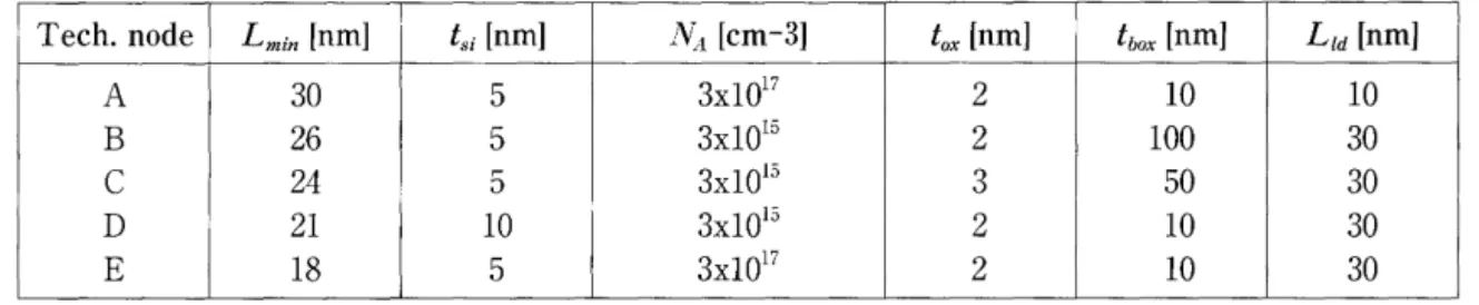
Table 1. Device parameters assumed in the simulations. Device parameters
Gate oxide thickness, t0x SOI layer thickness, tsi
Buried oxide layer thickness, tbox SOI doping concentration, NA Lateral diffusion length, L1d
Substrate doping concentration, Nsub Source/drain doping concentration, Ns/D Gate poly‑Si doping concentration, Ns;D
Values [unit] 2 ‑5 [n叫
5 ‑30 [nm] 10 ‑100 [nm] 3xl015 ‑lxl018 [cm‑3] 5 ‑30 [n叫
3xl017 [cm‑3] 4xl020 [cm‑3] 4xl020 [cm‑3]