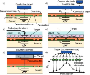
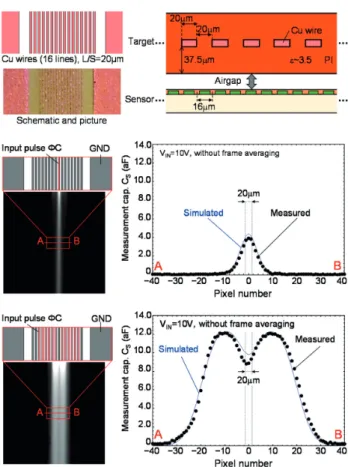
[Invite Paper] High Accuracy High Spatial Resolution and Real-Time CMOS Proximity Capacitance Image Sensor Technology and its Applications
全文
図
関連したドキュメント
In the following chapter, we examine our generalisation of pre-logical predicates by means of several examples, such as the case of traditional many-sorted algebras, the
In applications, the stability estimates for the solutions of the high order of accuracy di ff erence schemes of the mixed-type boundary value problems for hyperbolic equations
この chart の surface braid の closure が 2-twist spun terfoil と呼ばれている 2-knot に ambient isotopic で ある.4個の white vertex をもつ minimal chart
With hysteresis not enabled (see ALS_CONFIG register), the ALS_TH registers set the upper and lower interrupt thresholds of the ambient light detection window. Interrupt
The analog current sense pin in such an event will output the fault state current−typically higher than the currents sensed during normal operation and a high fault−state sense
With hysteresis not enabled (see ALS_CONFIG register), the ALS_TH registers set the upper and lower interrupt thresholds of the ambient light detection window. Interrupt
The analog to digital converter is a 7−bit A/D which can be used as an event recorder, an input voltage sampler, output voltage sampler, input current sampler, or output
Depending on the operation mode (Master or Slave), the pixel array of the image sensor requires different digital control signals.. The function of each signal is listed in
