Synthesis and Growth Mechanism of Two-
Dimensional Atomic Sheets of Hexagonal Boron Nitride
内田, 勇気
http://hdl.handle.net/2324/2236279
出版情報:九州大学, 2018, 博士(工学), 課程博士 バージョン:
権利関係:
Synthesis and Growth Mechanism of
Two-Dimensional Atomic Sheets of Hexagonal Boron Nitride
A Dissertation Presented to Interdisciplinary Graduate School of Engineering Sciences of Kyushu University
Yuki Uchida
2019
Abstract
Hexagonal boron nitride (h-BN), a layered material composed of boron (B) and nitrogen (N) atoms, is expected to be an ideal dielectric layer for two-dimensional (2D) materials due to its atomically smooth and dangling bond-free surface, low polarizable surface optical phonons, and a layered structure, contributing to bring out intrinsic physical, electrical, and optical properties of 2D materials. Most of the previous studies have used mechanically exfoliated h-BN flakes obtained from bulk h-BN crystals using adhesive tape. However, the size of the exfoliated h-BN flakes is relatively small (1-30
m) and they contain various thicknesses, limiting the developing of practical applications based on 2D materials, such as graphene and transition metal chalcogenides (TMCs). Chemical vapor deposition (CVD) utilizing catalytic substrates is expected to be a promising method to synthesize large-area h-BN film with controllable thickness and shape at low-cost. However, in contrast to CVD growth of monolayer graphene whose large scale growth has been reported by many groups, the CVD growth of h-BN with controlled thickness and lattice orientation has been a still challenging issue.
This thesis reports the epitaxial growth of monolayer h-BN on Cu(111) film and uniform growth of multilayer h-BN on Ni-Fe film in large-scale. In most of the previous works, polycrystalline metal catalysts have been used. Polycrystalline metal catalyst for the h-BN growth gives a h-BN sheet with different lattice orientations, resulting in the poorly connected small grains as well as inhomogeneous film thickness due to segregation from many grain boundaries existing in the metal catalyst. The Cu(111) film was prepared on a c-plane sapphire substrate by sputtering, allowing to grow highly oriented h-BN sheet with a monolayer thickness, as confirmed by scanning electron
microscope (SEM) and low-energy electron diffraction (LEED) measurements. Moreover, it was found that the epitaxially grown h-BN protects the Cu(111) surface from the oxidation in air in spite of its monolayer thickness.
In this thesis the uniform growth of multilayer h-BN using a Ni-Fe alloy film deposited on single-crystal spinel and sapphire substrates is also reported. The alloy film can tune the B and N solubilities in the metal catalyst and contribute to the controlling of the crystal structure during CVD process. This thesis also reveals the dynamics of h-BN growth on the alloy metal catalyst which is strongly dependent on the crystalline plane of the initial alloy. Moreover, the optical property of monolayer tungsten disulfide (WS2) was found to be significantly improved when the WS2 was grown on the CVD-grown multilayer h-BN.
The result indicates that the present CVD-grown h-BN can be effective as a substrate for various 2D materials. This work is expected greatly contribute to the further development of 2D materials-based devices and other applications.
Table of contents
Abstract
Table of contents Abbreviation
Chapter 1 – Introduction --- 1
1.1 History of boron nitride --- 1
1.1.1 Allotropes of boron nitride --- 1
1.1.2 Allotropes of low-dimensional boron nitride --- 4
1.2 h-BN: ideal dielectric layer for 2D materials --- 6
1.2.1 Atomically thin 2D materials --- 6
1.2.2 h-BN-based van der Waals (vdW) heterostructures --- 11
1.3 Purpose of the research --- 13
1.4 Outlines of this thesis --- 15
References ---16
Chapter 2 – Research trend in 2D materials --- 29
2.1 Why do 2D materials attract researchers attention? --- 29
2.2 Development of 2D materials research field --- 30
2.3 Research activities categorized by countries --- 32
2.3.1 Scientific papers --- 32
2.3.2 Patents --- 34
2.4 Active communities in 2D materials research --- 36
References --- 38
Chapter 3 – Properties and preparation method of h-BN --- 41
3.1 Structures and properties of h-BN--- 41
3.1.1 Structures --- 41
3.1.2 Lattice vibrations --- 42
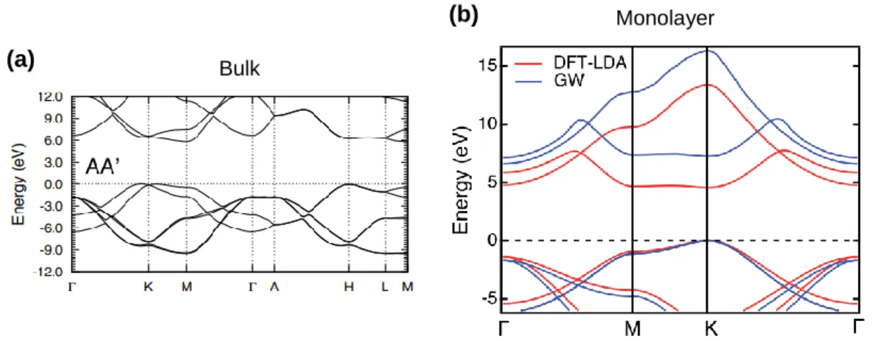
3.1.3 Electronic band structure --- 44
3.1.4 Dielectric properties --- 45
3.1.5 Surface roughness --- 47
3.1.6 Surface charged impurities --- 48
3.1.7 Surface optical phonons --- 49
3.1.8 Oxidation resistance --- 51
3.2 Synthesis of 2D h-BN sheets: Top down approach --- 52
3.2.1 Mechanical exfoliation --- 52
3.2.2 Liquid-phase exfoliation --- 53
3.3 Synthesis of 2D h-BN sheets: Bottom up approach --- 55
3.3.1 High pressure, high temperature (HPHT) method --- 55
3.3.2 Physical vapor deposition (PVD) --- 57
3.3.3 Chemical vapor deposition (CVD) --- 59
3.3.4 Metal catalysts for CVD growth of h-BN --- 60
3.3.5 Precursors used in CVD growth of h-BN --- 62
3.4 Theory of CVD growth --- 65
3.4.1 Boundary layer and gas diffusion --- 65
3.4.2 Nucleation of crystals on substrates --- 67
3.4.3 h-BN growth on metal catalysts with different solubility --- 69
3.4.4 Phase diagram of metals with B and N --- 71
References --- 73
Chapter 4 – Epitaxial CVD growth of monolayer h-BN on Cu(111)/sapphire substrate --- 83
4.1 Introduction --- 83
4.2 Experimental methods --- 85
4.2.1 Preparation of heteroepitaxial Cu(111) film and growth of h-BN --- 85
4.2.2 Characterization of h-BN --- 86
4.2.3 Fabrication of stacked graphene/h-BN heterostructures and graphene transistors --- 87
4.3 Results and discussion --- 88
4.3.1 Epitaxial growth of monolayer h-BN --- 88
4.3.2 LEED measurements --- 90
4.3.3 XPS and Raman measurements --- 93
4.3.4 Growth mechanism of monolayer h-BN --- 98
4.3.5 Graphene FETs --- 100
4.4 Conclusions --- 102
References --- 103
Chapter 5 – Controlled growth of large-area, uniform multilayer h-BN and application to 2D substrate --- 109
5.1 Introduction --- 111
5.2 Experimental methods --- 111
5.2.1 Preparation of Ni-Fe catalyst --- 111
5.2.2 CVD growth of multilayer h-BN --- 111
5.2.3 CVD growth for monolayer WS
2--- 112
5.2.4 Characterizations --- 112
5.3 Results and discussion --- 114
5.3.1 Synthesis of large-area and uniform multilayer h-BN --- 114
5.3.2 Comparison of different catalysts --- 120
5.3.3 Application of multilayer h-BN to 2D substrate --- 124
5.3.4 Mechanism of catalytic growth of multilayer h-BN --- 128
5.3.5 Multilayer h-BN growth on sapphire substrates --- 135
5.4 Conclusions --- 139
References --- 140
Chapter 6 – Conclusions and future outlook --- 143
6.1 Conclusions --- 143
6.2 Future outlook --- 144
References --- 146
Acknowledgment --- 149
List of publication --- 150
Abbreviation
0D: Zero-dimensional 1D: One-dimensional 2D: Two-dimensional
AFM: Atomic force microscopy APS: Ammonium persulfate
ARPES: Angle-resolved photoemission spectroscopy BSSE: Basis set superposition error
CB: Conduction band
CCD: Charge coupled device CDW: Charge density wave CL: Cathodoluminescence CVD: Chemical vapor deposition DFT: Density functional theory DOS: Density of states
EBSD: Electron back scattered diffraction EDX: Energy dispersive X-ray spectrometry EELS: Electron energy loss spectroscopy FET: field effect transistor
FIB: Focused-ion beam
FWHM: Full-width at half-maximum GB: Grain boundarie
HF: Hartree-fock
HOPG: Highly oriented pyrolytic graphite
HPHT: High pressure and high remperature IR: Infrared
LED: Light emitting diode
LEED: Low-energy electron diffraction
LMP2: Local second-order Møller-Plesset perturbation LO: Longitudinal-optical
LPE: Liquid phase exfoliation MBE: Molecular beam epitaxy
MOCVD: Metal organic chemical vapor deposition PBEsol: Perdew-Burke-Ernzerhof revised for solid PCT: Patent cooperation treaty
PDMS: Poly(dimethylsiloxane) PL: Photoluminescence
PMMA: Poly(methyl methacrylate) PVD: Physical vapor deposition
RDCP: Relative database citation potential RF: Radio frequency
RIP: Raw impact per paper published in the journal RMS: Root-mean-square
SEM: Scanning electron microscopy SNIP: Source normalized impact per paper SO: Surface optical
TEM: Transmission electron microscopy TMC: Transition metal chalcogenide
TMDC: Transition metal dichalcogenide TRT: Thermal release tape
VB: Valence band
WFC: Weighted fractional count
XPS: X-ray photoelectron spectroscopy bcc: Body-centered cubic
c-BN: Cubic boron nitride fcc: Face-centered cubic h-BN: hexagonal boron nitride hcp: Hexagonal close packed r-BN: Rhombohedral boron nitride vdW: van der Waals
w-BN: Wurtzite boron nitride
Chapter 1 Introduction
1.1 History of boron nitride
1.1.1 Allotropes of boron nitride
Boron nitride (BN) is an inorganic compound consisting of boron (B) and nitrogen (N) atoms with a stoichiometric ratio of 1. BN has several crystal structures, such as hexagonal BN (h-BN), rhombohedral BN (r-BN), cubic BN (c-BN), and wurtzite BN (w- BN). Some of these structures are similar to those of carbon allotropes (e.g. hexagonal:
graphite, cubic: diamond), because a B-N bond is isoelectronic with a C-C bond. For this similarity, sp2 and sp3 -bonded BN structures can exist.
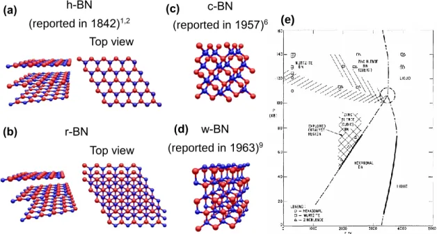
W. H. Balmain firstly synthesized boron nitride in 1842 by reacting H3BO3 and KCN.1,2 This synthesized boron nitride had a layered structure with the hexagonal lattice of B and N (h-BN shown in Figure 1a). B and N atoms form sp2 covalent bonds within a plane, while each layer is stacked with weak van der Waals (vdW) interaction. The stacking order of h-BN layer is AA’ stacking in which the N atoms are located on top of B atoms of the adjacent layers. A different type of stacking order of boron nitride is a rhombohedral structure (r-BN), whose stacking order is expressed as ABC stacking (Figure 1b). These layered structures show lubricity due to weak inter-layer vdW interaction. For instance, h-BN have been used as a solid lubricant for a long time.3 After the first h-BN synthesis reported by W. H. Balmain, many researchers started to study on synthesizing various BN compounds including h-BN due to the possibility of making carbon analogous structure (graphite).4,5 The first synthesis of c-BN, diamond-like
structure by sp3 covalent bods of B and N atoms, was reported by R. H. Wentorf in 1957.6 The cubic BN structure was synthesized from h-BN by applying extremely high pressure and high temperature (HPHT, 1800 °C and 8.6 GPa), being similar to diamond synthesis from graphite.7 Similar to diamond, c-BN is known as a hard material (second hardest material in the world) so that it is applicable to cutting tools for processing stiff materials.8 In 1963, the existence of wurtzite type BN (w-BN) was reported by Bundy and Wentorf.9 The synthesis of w-BN was also carried out under high pressure from h-BN, but this transformation occurred at much lower temperature (300 °C) than that used for c-BN synthesis. As shown in Figure 1-1e, the pressure-temperature phase diagram of boron nitride has several phase equilibrium lines, indicating the presence of different crystalline phases of boron nitride. These different BN structures have common excellent properties, such as high resistivity, thermal conductivity, and oxidation resistance. The physical properties of h-BN, c-BN, and w-BN are summarized in Table 1-1.10–17 Reflecting many
h-BN (reported in 1842)1,2
c-BN (reported in 1957)6
w-BN (reported in 1963)9 Top view
Top view
Figure 1-1 Atomic models of various BN structures. (a) h-BN, (b) r-BN, (c) c-BN, (d) w-BN. (e) Pressure-temperature phase diagram with the equilibrium lines.9
r-BN
(a) (e)
(c)
(b) (d)
attractive properties, industrial development of boron nitride has proceeded extensively, realizing many applications such as filler, crucible, lubricant, and catting tools.4,5
In the past two decades, the quality of boron nitride crystals has been significantly improved by employing highly purified solvent with extremely high temperature and pressure, mainly developed by Watanabe, Taniguchi, and Kanda.18 This method allows to synthesize single crystalline c-BN and h-BN which show an intense exciton related cathodoluminescence (CL) peak at around 200 nm. This enabled to determine the intrinsic band gap experimentally. It had not been considered that h-BN shows intense luminescence due to the indirect band gap nature, but the result suggested a direct band gap nature in h-BN.19 These reports stimulate further investigation of the band structure of h-BN20–28, and finally it was concluded again that h-BN has an indirect band gap in spite of its strong photoluminescence.20,29–31 Recently, application of h-BN to a substrate and/or a protection layer for two-dimensional (2D) materials as well as investigation of the optical properties of encapsulated 2D materials has been receiving increased interest, because the h-BN surface is atomically smooth and free of dangling bonds, which brings out the intrinsic properties of 2D materials32. This application of h-BN will be explained later in more details.
Table 1-1 Physical properties of three polymorphs of boron nitride. //c and Ʇc show the direction of parallel and normal to the c axis, respectively.
1.1.2 Allotropes of low-dimensional boron nitride
When material size becomes sufficiently small, typically 10 nm or less, the quantum confinement effect appears. This effect can be observed mainly by the change of the electronic and optical properties, which are deeply related to the electronic density of states (DOS), as shown in Figure 1-2a. For this, nanomaterials are fascinating objects for exploring new physical phenomena and also offer a possibility to create outstanding applications. In addition, surface area to volume ratio increases greatly with decreasing material size (Figure 1-2b), which is very useful for applications, such as catalyst, electrode for battery, and gas adsorbent. Carbon materials can form low-dimensional nanostructures, such as zero-dimensional (0D) fullerene, one-dimensional (1D) carbon nanotube, and 2D graphene. These kinds of low-dimensional structures of BN can be also observed, thanks to the similarity of a B-N bond to a C-C bond. These BN-based nanostructures have been actively studied, because the finding of new nanostructures is one of active fields in material science.33
The synthesis of 1D BN nanotube using an arc discharge method, similar to that used for the production of fullerene and carbon nanotube, was reported in 1995 by N. G.
Chopra et al.34 Like carbon nanotube, BN nanotube is composed of a h-BN sheet wrapped into a cylindrical tube (Figure 1-2c) and various chiralities can be formed, changing the band structure (also band gap).35 In addition to BN nanotube, 1D BN nanostructures, such as nanowires, nanofibers, nanorods and nanoribbons, based on h- BN have been reported.36–39 D. Golberg et al. reported the synthesis of 0D octahedral BN fullerene by electron beam irradiation to polygonal BN particles in 1998.40 Afterwards, various works on theoretical and experimental studies have been widely performed to find different forms of BN fullerene.41–46 The synthesis of 2D h-BN with monolayer
thickness was reported by reacting borazine on metal surfaces, including Ni(111), Pd(111), and Pr(111) by A. Nagashima et al. in 1995.47 Moreover, they investigated the electronic band structure of h-BN deposited on these metals by angle-resolved electron spectroscopy (ARPES) and found that h-BN is physisorbed on metal surfaces. As another 2D BN structure, nanomesh structure of BN was synthesized in 2004 by M.
Corso.48 Recently, research on 2D h-BN have been extensively performed in the world inspired by intensive reports on graphene and related 2D materials.
Figure 1-2 (a) Electron density of states (DOS) for a bulk 3D, 2D structured, 1D structured, and 0D structured materials. (b) Surface to volume ratio of a nanoparticle plotted against the volume. (c) Atomic models of low-dimensional BN nanostructures.
Quantum confinement effect
Increase of specific surface area
0D BN fullerene (reported in 1998)40
1D BN nanotube (reported in 1995)34
2D BN nanosheet (reported in 1995)47
(a) (b)
(c)
1.2 h-BN: an ideal dielectric sheet for 2D materials
1.2.1 Atomically thin 2D materials
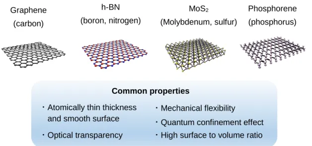
About 100 years ago, R. E. Peierls, L. D. Landau, and N. D. Mermin theoretically predicted that atomically thin 2D crystal cannot exist due to its instability.49–51 In spite of their theoretical prediction, thinnest 2D material, called graphene consisting of carbon honeycomb lattices with only one atom thickness, was experimentally prepared under ambient condition by K. S. Novoselov et al. in 2004.52 The atomic model of graphene is described in Figure 1-3. Surprisingly, this graphene flake was obtained by a simple mechanical exfoliation from highly-oriented pyrolytic graphite (HOPG) using adhesive tape. Few-layer graphene showed an exceptionally high carrier mobility (~10,000 cm2/Vs), which suggests such simple exfoliation method can produce high quality 2D materials (Figure 1-4a). Afterwards, they reported that monolayer graphene is a zero- gap semiconductor from the measured transport properties.53 These results infer that the charge carriers in graphene behave as massless Dirac fermions which is expressed by the Dirac equation instead of Schrödinger equation that describes the electronic properties of most of the materials (Figure 1-4b).53 The discovery of graphene and its quantum confinement effects attracted great interest in 2D system. At the early stage of the graphene research, peculiar physical properties of graphene, such as a massless charge carrier, high optical transparency, high mechanical flexibility, and high mechanical strength, were extensively studied.54 These outstanding properties make graphene a promising candidate as main component in next generation devices.55
A few years later, scientists also paid attention to other 2D materials. Various layered materials were peeled off to form atomically-thin flakes, like graphene56, leading to many important findings in 2D materials reported to date. Figure 1-3 shows atomic
structures of representative 2D materials. Table 1-257 lists a wide variety of 2D materials including metal oxide. Among them, 2D transition metal chalcogenides (TMCs) have been widely studied. In 2010, unique indirect to direct band gap transition was reported for molybdenum disulfide (MoS2), a family of TMCs.58,59 With decreasing the number of layers of MoS2, the band structure of MoS2 gradually changes and eventually it forms a direct band gap when it becomes monolayer. Thus, the monolayer MoS2 shows strong exciton-related photoluminescence, while bilayer and multilayer MoS2 do not show strong luminescence due to indirect gap nature (Figure 1-4c).59 Because monolayer
Figure 1-3 Atomic structures of representative 2D materials and the common properties of these 2D materials.
Graphene (carbon)
h-BN (boron, nitrogen)
MoS2
(Molybdenum, sulfur)
Phosphorene (phosphorus)
・Mechanical flexibility
・Optical transparency
・Atomically thin thickness
and smooth surface ・Quantum confinement effect Common properties
・High surface to volume ratio
Table 1-2 List of various 2D materials (modified from ref.57)
TMCs, such as MoS2, tungsten disulfide (WS2), and tungsten diselenide (WSe2), are materials having the strong interaction of charges, tightly bound trions (binding energy is
~20 meV for MoS2) and biexitons (binding energy is ~52 meV for WSe2) were experimentally observed,60,61 offering a new platform to explore many-body effects (Figure 1-4g). Moreover, due to the lack of inversion symmetry in odd numbers of layers of MoS2, valley polarization was observed by optical pumping with circularly polarized light, which enables us to manipulate valley degree of freedom as an information carrier like charge carriers and spin polarized carriers (Figure 1-4h).62–65 These experimental observations carve out new possibility that 2D TMCs are suitable for photonics, optoelectronics, and valleytronics.
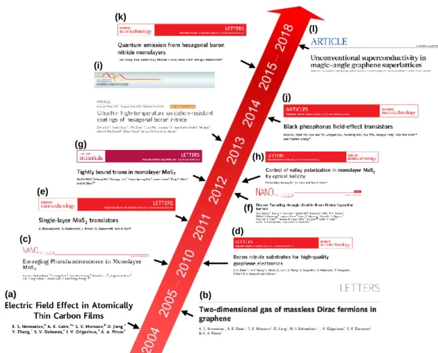
Figure 1-4 Representative reports regarding important findings of physical properties in 2D materials.
(a) (b)
(c) (d)
(e)
(f) (g)
(h) (i)
(j) (k)
(l)
Demands for electronic devices, such as low power consumption with high performance, device flexibility, and optical transparency, 2D materials have also attracted great attention.66 For example, it was found that monolayer MoS2 shows a high on/off ratio of ~108 with carrier mobility of ~217 cm2/Vs in spite that the channel is only a few atom thickness (Figure 1-4e).67 Therefore, 2D semiconductors have attracted a great interest from the expectation for future electronics, because it is likely that it can overcome the limitation of performance from the short channel effect, which is one of main issues in ultra-scale devices. In 2014, it was reported that the carrier mobility of phosphorene, mono or few-layer black phosphorus, is higher than that of TMCs, while having an enough band gap for switching of transistors (observed mobility was ~1,000 cm2/Vs with an on/off ratio of ~105) (Figure 1-4j).68
2D superconductivity has been widely studied for a long time, because of its wealth of quantum phenomena.69 Recent progress of synthesis of various 2D materials made the 2D superconductivity a hot topic again. In 2015, superconductivity in monolayer NbSe2 produced by mechanical exfoliation was observed.70,71 Moreover, it was found that this 2D NbSe2 shows enhanced charge-density-wave (CDW) due to enhanced electron-phonon interactions. To modulate superconducting transition temperature (Tc) in 2D system, electro-static doping via ion gating using ionic liquid was found to be an excellent approach. For instance, ZrNCl and MoS2 measured at different gate voltages showed increased Tc.72,73 Very recently, inspired by the theoretical prediction,74 superconducting behavior were observed in twisted bilayer graphene with a specific stacking angle, which is called a magic angle (in spite of the conductive nature of graphene),75 which was realized by precise angle-controlled transfer technique.76–78 This is because under the magic angle strongly correlated electrons due to the flat band make
superconducting state that can be induced by applied gate voltage. This report stimulates tremendous recent interest in moiré superlattices using 2D materials (Figure 1-4l).79–90
In 2017, magnetic order in 2D materials was found by two research groups.91,92 Cheng Gong et al. discovered ferromagnetism in Cr2Ge2Te6 atomic layers.91 In contrast to bulk materials, it was found that transition temperature from paramagnetic and ferromagnetic states in Cr2Ge2Te6 atomic layers can be controlled by small magnetic field (smaller than 0.3 tesla). Huang et al. demonstrated ferromagnetism in CrI3 with even monolayer thickness.92 However, these magnetisms were observed at cryogenic temperatures. More recently, M. Bonilla et al. reported that monolayer VSe2 deposited on graphite and MoS2 substrates by MBE method shows ferromagnetism at room temperature.93 Thanks to the discovery of these 2D magnets, it is expected that further efforts on studying 2D magnetic materials provide new kinds of devices, such as 2D spin valves and single-photon sources with electric polarization control.94
2D h-BN is an attractive material as a tunnel barrier layer for charge carriers and spin-polarized electrons due to its large band gap, atomically flat surface, atom-level thickness uniformity, and controllable thickness. Several fundamental studies regarding electron tunneling through h-BN layers suggested that it has great potential for tunneling devices,95,96 which stimulates various studies on devices utilizing tunneling effect through 2D h-BN (Figure 1-4f).97–101 Moreover, chemical inertness and impermeable in-plane structure of h-BN make it a fascinating material as a passivation layer. For example, several studies reported that 2D h-BN prevents certain 2D materials from oxidation even when monolayer h-BN was used (Figure 1-4i).102,103 Also, the application of h-BN to passivation barriers for ions was demonstrated in several fields, such as biology, electronics, and optoelectronics.104–107 Recently, it is also proposed that h-BN is a
promising material for 2D quantum light emitter (Figure 1-4k),108 ultrabright , photostable, and room temperature quantum emitter like diamond partly due to a wide band gap (~6 eV) and clear structure.109 For this, there are several promising applications based on quantum emission from h-BN including quantum computing, quantum sensing, and platform to explore basic quantum phenomena.108 More importantly, the application which attracts the most attention nowadays is utilization as a dielectric layer to bring out intrinsic physical properties of other 2D materials, such as graphene and TMCs (Figure 1-4d).110 Detailed explanation related to this point will be described in the next section.
1.2.2 h-BN-based van der Waals (vdW) heterostructures
As mentioned in the 1.2.1 section, Most of 2D materials can exist under ambient condition. However, due to atomic thickness and high surface area, 2D materials are highly sensitive to their environment, including changes in temperature, humidity, adsorbates, and charged impurities, which hinders the observation of intrinsic physical properties of 2D materials. This is because most or even all of the atoms of 2D materials locate on the surface of other materials, unlike bulk materials. An example of this inherent sensitivity of 2D materials is illustrated in Figure 1-5 (graphene and its heterostructures with h-BN). Carrier mobility in graphene/SiO2 is usually limited by the surface roughness, charged impurities, dangling bonds, and optical phonons of the underlying SiO2 surface (most of substrate materials have similar surfaces interacting with 2D materials).111–116 In addition, the electronic properties of graphene is affected by physisorption of molecules.117 In certain cases, this phenomenon can be advantageous when 2D materials are used as gas sensor. However, the properties of the 2D materials are generally degraded by physisorbed oxygen and water
when exposed to ambient. Therefore, it is essential to eliminate the influences suffered from the environment in 2D materials.
To solve these issues, h-BN is expected to be an ideal dielectric substrate and protection layer for 2D materials. This is because the h-BN surface is atomically smooth and free from dangling bonds, and h-BN can be stacked with other 2D materials via weak van der Waals (vdW) interaction, which is generally called as vdW heterostructue.
Actually, the introduction of h-BN to the interface between a 2D material and substrate surface significantly improves the physical properties of the 2D materials. For example, the carrier mobility of graphene can be increased from 17,000 cm2/Vs to 60,000 cm2/Vs, by simply introducing multilayer h-BN between a graphene channel and SiO2 surface (Figure 1-5).110,118 This mobility can be further increased to 140,000 cm2/Vs, which is Figure 1-5 Carrier mobilities of graphene transistors combined with multilayer h-BN layers. is measured carrier mobility of graphene.133-135
· Slightly rough
· Charged impurities
· dangling bonds
· Highly polarized optical phonons
SiO2 surface h-BN surface
· Atomically smooth
· Dangling bond-free
· Lowly polarized optical phonons
· Impermeable in-plane structure
Graphene/SiO2 Graphene/h-BN/SiO2 h-BN/Graphene/h-BN/SiO2
(RT): 140,000 cm2/Vs 119)
(theoretical limitation: 200,000 cm2/Vs)
(RT): 60,000 cm2/Vs 110)
(RT): 17,000 cm2/Vs 118)
Limited carrier mobility mainly due to scattering effect by SiO2 surface
Bottom h-BN Realization of clean interface and screening of long range interaction from SiO2 surface
Top h-BN
Realization of clean interface on top side and protection from adsorbates
close to the theoretical limit value, by encapsulating the graphene channel with h-BN using the improved transfer process.119
The carrier mobility of TMCs was also increased by h-BN, reaching 1,000-34,000 cm2/Vs at low temperatures.120 Furthermore, optical properties of TMCs can be substantially improved by growing WS2 on h-BN instead of SiO2 surface.121 The photoluminescence (PL) of WS2 becomes much stronger and sharper (full width at half maximum (FWHM) is 26 meV) on h-BN, as compared with that grown on SiO2 substrate surface (61 meV).121 Such drastic improvement by h-BN is accounted for by the reduction of the influences (charged impurities, polar optical phonons, and relatively rough surface) from the underlying substrates (e.g. SiO2/Si substrate). As another important aspect, 2D materials encapsulated by h-BN becomes stable because of the gas barrier property of h-BN. Actually, it was demonstrated that black phosphorous, very easy to be oxidized in air, can be stabilized by covering with h-BN.122 Due to such large contribution, h-BN is now widely used in both fundamental study and applications of 2D materials. Therefore, h-BN is a highly desirable dielectric layer for applications to various 2D materials.
1.3 Purpose of the research
Since the first report on the significant increase of the graphene’s carrier mobility by h-BN, fundamental studies on the h-BN-based vdW heterostructures have been extensively performed in the world. Most of the studies have used mechanically exfoliated h-BN flakes. Although the exfoliated h-BN flakes have high crystalline quality, h-BN flake size is small and its thickness is not uniform on a substrate. Now h-BN is an essential material in the field of 2D materials. Therefore, development of the scalable and low cost fabrication of vdW heterostructure using h-BN is highly required for practical
applications. Different types of h-BN production methods have been reported.32 For instance, liquid-phase exfoliation is a good candidate for producing large amount of h- BN flakes suitable for wet processes to make large-area h-BN sheets.123 However, the quality of flakes is low and also the realization of good connection between flakes is difficult, preventing the application to 2D substrate. Bottom up approach has a great potential to make high quality h-BN with controllable shape, stacking order, and thickness in large-scale. In particular, chemical vapor deposition (CVD) method employing catalytic
Figure 1-6 Novel points and achievement in this thesis
Previous studies
Studies in this thesis
Growth of h-BN on polycrystalline metal foils103,124–135
⇒Random h-BN orientation
Growth of multilayer h-BN on polycrystalline Fe foils136,137
⇒Non-uniform h-BN thickness
Large-area epitaxial growth of h- BN using Cu(111) film
Growth of uniform multilayer h-BN using Ni-Fe film
Significant enhancement of optical properties of WS2 using CVD multilayer h-BN
Chapter 4
Chapter 5
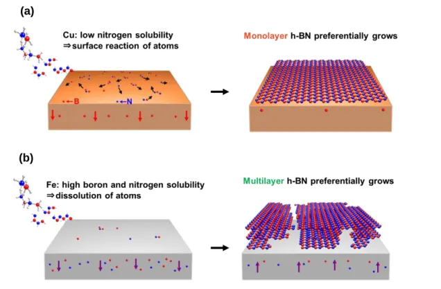
substrate is expected to meet above requirements so that many researchers have studied the synthesis of h-BN by CVD method. However, in spite of the significant efforts, the controlled synthesis of h-BN has not achieved so far. For realizing the synthesis of high-quality h-BN by CVD method, metal catalyst becomes very important. For example, the selection of metals with suitable crystal structure, melting point, and solubilities of B and N is important to control h-BN growth. Moreover, structural morphologies of metals, such as density of grain boundaries and crystal planes, are also important factors. In previous literatures, polycrystalline meal foils have been mainly used, but these foils produced randomly oriented h-BN grains.103,124–135 Also, uniform growth of multilayer h- BN is still a challenging issue, because highly controlled B, N dissolution and segregation processes are required.136,137 In this thesis, CVD growth and mechanisms of monolayer, epitaxially aligned h-BN on Cu(111) film and uniform multilayer h-BN on Ni-Fe alloy film are extensively investigated.
1.4 Outline of this thesis
This thesis consists of two main parts, (1) epitaxial CVD growth of monolayer h-BN on Cu(111) film and (2) uniform growth of multilayer h-BN on Ni-Fe alloy film and its growth mechanism. Prior to the experimental results and discussion regarding these main parts, I would like to describe research trends in 2D materials to show how this research field has advanced in Chapter 2. After that, several properties of h-BN and details of preparation methods, especially CVD method, are described in Chapter 3.
Chapter 4 and 5 demonstrate epitaxial growth of monolayer h-BN on Cu(111) film in large-scale and growth of uniform multilayer h-BN on Ni-Fe alloy film, respectively. Finally, I conclude this thesis and describe future outlook in Chapter 6.
References
1. Balmain, W. H. Observations on the formation of compounds of boron and silicon with nitrogen and certain metals. Philos. Mag. J. Series 3, 21, 270–277 (1842).
2. Balmain, W. H. Bemerkungen über die bildung von verbindungen des bors und siliciums mit stickstoff und gewissen metallen. J. Prakt. Chem. 27, 422–430 (1842).
3. Watanabe, S., Miyake, S. and Murakawa, M. Tribological properties of cubic, amorphous and hexagonal boron nitride films. Surf. Coat. Technol. 49, 406–410 (1991).
4. Vel, L., Demazeau, G. and Etourneau, J. Cubic boron nitride: synthesis, physicochemical properties and applications. Mater. Sci. Eng. B 10, 149–164 (1991).
5. Lipp, A., Schwetz, K. A. and Hunold, K. Hexagonal boron nitride: Fabrication, properties and applications. J. Eur. Ceram. Soc. 5, 3–9 (1989).
6. Wentorf, R. H. Cubic form of boron nitride. J. Chem. Phys. 26, 956–956 (1957).
7. Bundy, F. P., Hall, H. T., Strong, H. M. and Jun, R. H. W. Man-made diamonds. Nature 176, 51–55 (1955).
8. Murakawa, M. Surface coatings of super hard materials for tool applications. Mater.
Sci. Forum 246, 1-28 (1997).
9. Bundy, F. P. and Wentorf, R. H. Direct transformation of hexagonal boron nitride to denser forms. J. Chem. Phys. 38, 1144–1149 (1963).
10. Xu, Y.-N. and Ching, W. Y. Calculation of ground-state and optical properties of boron nitrides in the hexagonal, cubic, and wurtzite structures. Phys. Rev. B 44, 7787–7798 (1991).
11. Edgar, J. H., Smith, D. T., Eddy, C. R., Carosella, C. A. and Sartwell, B. D. c-Boron–
aluminum nitride alloys prepared by ion-beam assisted deposition. Thin Solid Films 298, 33–38 (1997).
12. Ohba, N., Miwa, K., Nagasako, N. and Fukumoto, A. First-principles study on
structural, dielectric, and dynamical properties for three BN polytypes. Phys. Rev. B 63, 115207 (2001).
13. Soma, T., Sawaoka, A. and Saito, S. Characterization of wurtzite type boron nitride synthesized by shock compression. Mat. Res. Bull. 9, 755-762 (1974).
14. Li, L. H., Cervenka, J., Watanabe, K., Taniguchi, T. and Chen, Y. Strong oxidation resistance of atomically thin boron nitride nanosheets. ACS Nano 8, 1457–1462 (2014).
15. Xiang-Fen Jiang, Q. W. and Xiang-Fen Jiang, Q. W. Recent progress on fabrications and applications of boron nitride nanomaterials: A review. J. Mater. Sci. Technol. 31, 589–598 (2015).
16. Chen, L. et al. Thermal conductivity performance of polypropylene composites filled with polydopamine-functionalized hexagonal boron nitride. PLOS ONE 12, e0170523 (2017).
17. Narayan, J., Bhaumik, A., Gupta, S., Haque, A. and Sachan, R. Progress in Q-carbon and related materials with extraordinary properties. Mater. Res. Lett. 6, 353–364 (2018).
18. Watanabe, K., Taniguchi, T. and Kanda, H. Ultraviolet luminescence spectra of boron nitride single crystals grown under high pressure and high temperature. Phys. Status Solidi A 201, 2561–2565 (2004).
19. Watanabe, K., Taniguchi, T. and Kanda, H. Direct-bandgap properties and evidence for ultraviolet lasing of hexagonal boron nitride single crystal. Nat. Mater. 3, 404–409 (2004).
20. Arnaud, B., Lebègue, S., Rabiller, P. and Alouani, M. Huge excitonic effects in layered hexagonal boron nitride. Phys. Rev. Lett. 96, 026402 (2006).
21. Wirtz, L., Marini, A. and Rubio, A. Excitons in boron nitride nanotubes: dimensionality effects. Phys. Rev. Lett. 96, 126104 (2006).
22. Giovannetti, G., Khomyakov, P. A., Brocks, G., Kelly, P. J. and van den Brink, J.
Substrate-induced band gap in graphene on hexagonal boron nitride: ab initio density functional calculations. Phys. Rev. B 76, 073103 (2007).
23. Kubota, Y., Watanabe, K., Tsuda, O. and Taniguchi, T. Deep ultraviolet light-emitting hexagonal boron nitride synthesized at atmospheric pressure. Science 317, 932–934 (2007).
24. Evans, D. A. et al. Determination of the optical band-gap energy of cubic and hexagonal boron nitride using luminescence excitation spectroscopy. J. Phys.:
Condens. Matter 20, 075233 (2008).
25. Park, C.-H. and Louie, S. G. Energy gaps and stark effect in boron nitride nanoribbons. Nano Lett. 8, 2200–2203 (2008).
26. Gao, R. et al. High-yield synthesis of boron nitride nanosheets with strong ultraviolet cathodoluminescence emission. J. Phys. Chem. C 113, 15160–15165 (2009).
27. Watanabe, K., Taniguchi, T., Niiyama, T., Miya, K. and Taniguchi, M. Far-ultraviolet plane-emission handheld device based on hexagonal boron nitride. Nat. Photonics 3, 591–594 (2009).
28. Yu, J. et al. Vertically aligned boron nitride nanosheets: chemical vapor synthesis, ultraviolet light emission, and superhydrophobicity. ACS Nano 4, 414–422 (2010).
29. Watanabe, K. and Taniguchi, T. Jahn-Teller effect on exciton states in hexagonal boron nitride single crystal. Phys. Rev. B 79, 193104 (2009).
30. Gao, S.-P. Crystal structures and band gap characters of h-BN polytypes predicted by the dispersion corrected DFT and GW method. Solid State Commun. 152, 1817–
1820 (2012).
31. Cassabois, G., Valvin, P. and Gil, B. Hexagonal boron nitride is an indirect bandgap semiconductor. Nat. Photonics 10, 262–266 (2016).
32. Zhang, K., Feng, Y., Wang, F., Yang, Z. and Wang, J. Two dimensional hexagonal
boron nitride (2D-hBN): synthesis, properties and applications. J. Mater. Chem. C 5, 11992–12022 (2017).
33. Pakdel, A., Bando, Y. and Golberg, D. Nano boron nitride flatland. Chem. Soc. Rev.
43, 934–959 (2014).
34. Chopra, N. G. et al. Boron nitride nanotubes. Science 269, 966–967 (1995).
35. Golberg, D. et al. Boron nitride nanotubes and nanosheets. ACS Nano 4, 2979–2993 (2010).
36. Chen, Y. J., Zhang, H. Z. and Chen, Y. Pure boron nitride nanowires produced from boron triiodide. Nanotechnology 17, 786 (2006).
37. Zhang, H., Yu, J., Chen, Y. and Gerald, J. F. Conical boron nitride nanorods synthesized via the ball-milling and annealing method. J. Amer. Ceram. Soc. 89, 675–
679 (2006).
38. Chen, Z.-G. et al. Novel boron nitride hollow nanoribbons. ACS Nano 2, 2183–2191 (2008).
39. Qiu, Y. et al. Synthesis of continuous boron nitride nanofibers by solution coating electrospun template fibers. Nanotechnology 20, 345603 (2009).
40. Golberg, D., Bando, Y., Stéphan, O. and Kurashima, K. Octahedral boron nitride fullerenes formed by electron beam irradiation. Appl. Phys. Lett. 73, 2441–2443 (1998).
41. Alexandre, S. S., Mazzoni, M. S. C. and Chacham, H. Stability, geometry, and electronic structure of the boron nitride B36N36 fullerene. Appl. Phys. Lett. 75, 61–63 (1999).
42. Pokropivny, V. V. et al. Boron nitride analogs of fullerenes (the fulborenes), nanotubes, and fullerites (the fulborenites). J. Solid State Chem. 154, 214–222 (2000).
43. Oku, T., Kuno, M., Kitahara, H. and Narita, I. Formation, atomic structures and properties of boron nitride and carbon nanocage fullerene materials. Int. J. Inorg.
Mater. 3, 597–612 (2001).
44. Oku, T., Nishiwaki, A., Narita, I. and Gonda, M. Formation and structure of B24N24
clusters. Chem. Phys. Lett. 380, 620–623 (2003).
45. Oku, T., Nishiwaki, A. and Narita, I. Formation and atomic structure of B12N12
nanocage clusters studied by mass spectrometry and cluster calculation. Sci. Technol.
Adv. Mater. 5, 635–638 (2004).
46. Monajjemi, M. and Boggs, J. E. A new generation of BnNn rings as a supplement to boron nitride tubes and cages. J. Phys. Chem. A 117, 1670–1684 (2013).
47. Nagashima, A., Tejima, N., Gamou, Y., Kawai, T. and Oshima, C. Electronic structure of monolayer hexagonal boron nitride physisorbed on metal surfaces. Phys. Rev. Lett.
75, 3918–3921 (1995).
48. Corso, M. et al. Boron nitride nanomesh. Science 303, 217–220 (2004).
49. Peierls, R. E. Helv. Phys. Acta 7, 81 (1923).
50. Landau, L. D. Zur theorie der phasenumwandlungen Ⅱ. Phys. Z. Sowjet. 11, 26-35 (1937).
51. Mermin, N. D. Crystalline order in two dimensions. Phys. Rev. 176, 250–254 (1968).
52. Novoselov, K. S. et al. Electric field effect in atomically thin carbon films. Science 306, 666–669 (2004).
53. Novoselov, K. S. et al. Two-dimensional gas of massless Dirac fermions in graphene.
Nature 438, 197–200 (2005).
54. Geim, A. K. and Novoselov, K. S. The rise of graphene. Nat. Mater. 6, 183–191 (2007).
55. Schwierz, F. Graphene transistors. Nat. Nanotechnol. 5, 487–496 (2010).
56. Novoselov, K. S. et al. Two-dimensional atomic crystals. Proc. Natl. Acad. Sci. U.S.A.
102, 10451–10453 (2005).
57. Geim, A. K. and Grigorieva, I. V. Van der Waals heterostructures. Nature 499, 419–
425 (2013).
58. Mak, K. F., Lee, C., Hone, J., Shan, J. and Heinz, T. F. Atomically thin MoS2: a new direct-gap semiconductor. Phys. Rev. Lett. 105, 136805 (2010).
59. Splendiani, A. et al. Emerging photoluminescence in monolayer MoS2. Nano Lett. 10, 1271–1275 (2010).
60. Mak, K. F. et al. Tightly bound trions in monolayer MoS2. Nat. Mater. 12, 207–211 (2013).
61. You, Y. et al. Observation of biexcitons in monolayer WSe2. Nat. Phys. 11, 477–481 (2015).
62. Cao, T. et al. Valley-selective circular dichroism of monolayer molybdenum disulphide.
Nat. Commun. 3, 887 (2012).
63. Mak, K. F., He, K., Shan, J. and Heinz, T. F. Control of valley polarization in monolayer MoS2 by optical helicity. Nat. Nanotechnol. 7, 494–498 (2012).
64. Zeng, H., Dai, J., Yao, W., Xiao, D. and Cui, X. Valley polarization in MoS2 monolayers by optical pumping. Nat. Nanotechnol. 7, 490–493 (2012).
65. Suzuki, R. et al. Valley-dependent spin polarization in bulk MoS2 with broken inversion symmetry. Nat. Nanotechnol. 9, 611–617 (2014).
66. Fiori, G. et al. Electronics based on two-dimensional materials. Nat. Nanotechnol. 9, 768–779 (2014).
67. Radisavljevic, B., Radenovic, A., Brivio, J., Giacometti, V. and Kis, A. Single-layer MoS2 transistors. Nat. Nanotechnol. 6, 147–150 (2011).
68. Li, L. et al. Black phosphorus field-effect transistors. Nat. Nanotechnol. 9, 372–377 (2014).
69. Saito, Y., Nojima, T. and Iwasa, Y. Highly crystalline 2D superconductors. Nat. Rev.
Mater. 2, 16094 (2017).
70. Cao, Y. et al. Quality heterostructures from two-dimensional crystals unstable in air by their assembly in inert atmosphere. Nano Lett. 15, 4914–4921 (2015).
71. Xi, X. et al. Strongly enhanced charge-density-wave order in monolayer NbSe2. Nat.
Nanotechnol. 10, 765–769 (2015).
72. Ye, J. T. et al. Liquid-gated interface superconductivity on an atomically flat film. Nat.
Mater. 9, 125–128 (2010).
73. Ye, J. T. et al. Superconducting dome in a gate-tuned band insulator. Science 338, 1193–1196 (2012).
74. Bistritzer, R. and MacDonald, A. H. Moire bands in twisted double-layer graphene.
Proc. Natl. Acad. Sci. U.S.A. 108, 12233–12237 (2011).
75. Cao, Y. et al. Unconventional superconductivity in magic-angle graphene superlattices. Nature 556, 43–50 (2018).
76. Cao, Y. et al. Superlattice-induced insulating states and valley-protected orbits in twisted bilayer graphene. Phys. Rev. Lett. 117, 116804 (2016).
77. Kim, K. et al. van der Waals heterostructures with high accuracy rotational alignment.
Nano Lett. 16, 1989–1995 (2016).
78. Kim, K. et al. Tunable moiré bands and strong correlations in small-twist-angle bilayer graphene. Proc. Natl. Acad. Sci. U.S.A. 114, 3364–3369 (2017).
79. Dodaro, J. F., Kivelson, S. A., Schattner, Y., Sun, X. Q. and Wang, C. Phases of a phenomenological model of twisted bilayer graphene. Phys. Rev. B 98, 075154 (2018).
80. Efimkin, D. K. and MacDonald, A. H. Helical network model for twisted bilayer graphene. Phys. Rev. B 98, 035404 (2018).
81. Fidrysiak, M., Zegrodnik, M. and Spałek, J. Unconventional topological superconductivity and phase diagram for an effective two-orbital model as applied to twisted bilayer graphene. Phys. Rev. B 98, 085436 (2018).
82. Guo, H., Zhu, X., Feng, S. and Scalettar, R. T. Pairing symmetry of interacting fermions on a twisted bilayer graphene superlattice. Phys. Rev. B 97, 235453 (2018).
83. Kang, J. and Vafek, O. Symmetry, maximally localized wannier states, and a low-
energy model for twisted bilayer graphene narrow bands. Phys. Rev. X 8, 031088 (2018).
84. Koshino, M. et al. Maximally localized wannier orbitals and the extended hubbard model for twisted bilayer graphene. Phys. Rev. X 8, 031087 (2018).
85. Ochi, M., Koshino, M. and Kuroki, K. Possible correlated insulating states in magic- angle twisted bilayer graphene under strongly competing interactions. Phys. Rev. B 98, 081102 (2018).
86. Ribeiro-Palau, R. et al. Twistable electronics with dynamically rotatable heterostructures. Science 361, 690–693 (2018).
87. Thomson, A., Chatterjee, S., Sachdev, S. and Scheurer, M. S. Triangular antiferromagnetism on the honeycomb lattice of twisted bilayer graphene. Phys. Rev.
B 98, 075109 (2018).
88. Xu, C. and Balents, L. Topological superconductivity in twisted multilayer graphene.
Phys. Rev. Lett. 121, 087001 (2018).
89. Yuan, N. F. Q. and Fu, L. Model for the metal-insulator transition in graphene superlattices and beyond. Phys. Rev. B 98, 045103 (2018).
90. Zou, L., Po, H. C., Vishwanath, A. and Senthil, T. Band structure of twisted bilayer graphene: Emergent symmetries, commensurate approximants, and Wannier obstructions. Phys. Rev. B 98, 085435 (2018).
91. Gong, C. et al. Discovery of intrinsic ferromagnetism in two-dimensional van der Waals crystals. Nature 546, 265–269 (2017).
92. Huang, B. et al. Layer-dependent ferromagnetism in a van der Waals crystal down to the monolayer limit. Nature 546, 270–273 (2017).
93. Bonilla, M. et al. Strong room-temperature ferromagnetism in VSe2 monolayers on van der Waals substrates. Nat. Nanotechnol. 13, 289 (2018).
94. 2D magnetism gets hot. Nat. Nanotechnol. 13, 269 (2018).
95. Lee, G.-H. et al. Electron tunneling through atomically flat and ultrathin hexagonal boron nitride. Appl. Phys. Lett. 99, 243114 (2011).
96. Britnell, L. et al. Electron tunneling through ultrathin boron nitride crystalline barriers.
Nano Lett. 12, 1707–1710 (2012).
97. Britnell, L. et al. Field-effect tunneling transistor based on vertical graphene heterostructures. Science 335, 947–950 (2012).
98. Kamalakar, M. V., Dankert, A., Bergsten, J., Ive, T. and Dash, S. P. Enhanced tunnel spin injection into graphene using chemical vapor deposited hexagonal boron nitride.
Sci. Rep. 4, 6146 (2014).
99. Vu, Q. A. et al. Two-terminal floating-gate memory with van der Waals heterostructures for ultrahigh on/off ratio. Nat. Commun. 7, 12725 (2016).
100. Wang, J. et al. High mobility MoS2 transistor with low schottky barrier contact by using atomic thick h-BN as a tunneling layer. Adv. Mater. 28, 8302–8308 (2016).
101. Piquemal-Banci, M. et al. 2D-MTJs: introducing 2D materials in magnetic tunnel junctions. J. Phys. D: Appl. Phys. 50, 203002 (2017).
102. Liu, Z. et al. Ultrathin high-temperature oxidation-resistant coatings of hexagonal boron nitride. Nat. Commun. 4, 2541 (2013).
103. Sinha, S., Takabayashi, Y., Shinohara, H. and Kitaura, R. Simple fabrication of air- stable black phosphorus heterostructures with large-area hBN sheets grown by chemical vapor deposition method. 2D Mater. 3, 035010 (2016).
104. Parra, C. et al. Suppressing bacterial interaction with copper surfaces through graphene and hexagonal-boron nitride coatings. ACS Appl. Mater. Interfaces 7, 6430–
6437 (2015).
105. Ergen, O., Gilbert, S. M., Turner, S. J. and Zettl, A. Hexagonal boron nitride as a cationic diffusion barrier to form a graded band gap perovskite heterostructure. Phys.
Status Solidi B 253, 2478–2480 (2016).
106. Lo, C.-L. et al. Studies of two-dimensional h-BN and MoS2 for potential diffusion barrier application in copper interconnect technology. npj 2D Mater. and Appl. 1, 42 (2017).
107. Chilkoor, G. et al. Hexagonal boron nitride: the thinnest insulating barrier to microbial corrosion. ACS Nano 12, 2242–2252 (2018).
108. Aharonovich, I. and Toth, M. Quantum emitters in two dimensions. Science 358, 170–171 (2017).
109. Aharonovich, I. et al. Diamond-based single-photon emitters. Rep. Prog. Phys. 74, 076501 (2011).
110. Dean, C. R. et al. Boron nitride substrates for high-quality graphene electronics. Nat.
Nanotechnol. 5, 722–726 (2010).
111. Hwang, E. H., Adam, S. and Sarma, S. D. Carrier transport in two-dimensional graphene layers. Phys. Rev. Lett. 98, 186806 (2007).
112. Ishigami, M., Chen, J. H., Cullen, W. G., Fuhrer, M. S. and Williams, E. D. Atomic structure of graphene on SiO2. Nano Lett. 7, 1643–1648 (2007).
113. Chen, J.-H., Jang, C., Xiao, S., Ishigami, M. and Fuhrer, M. S. Intrinsic and extrinsic performance limits of graphene devices on SiO2. Nat. Nanotechnol. 3, 206–209 (2008).
114. Fratini, S. and Guinea, F. Substrate-limited electron dynamics in graphene. Phys.
Rev. B 77, 195415 (2008).
115. Katsnelson, M. I. and Geim, A. K. Electron scattering on microscopic corrugations in graphene. Phil. Trans. R. Soc. A 366, 195–204 (2008).
116. Morozov, S. V. et al. Giant intrinsic carrier mobilities in graphene and its bilayer.
Phys. Rev. Lett. 100, 016602 (2008).
117. Wehling, T. O. et al. Molecular doping of graphene. Nano Lett. 8, 173–177 (2008).
118. Hong, X., Zou, K. and Zhu, J. Quantum scattering time and its implications on scattering sources in graphene. Phys. Rev. B 80, 241415 (2009).
119. Wang, L. et al. One-dimensional electrical contact to a two-dimensional material.
Science 342, 614–617 (2013).
120. Cui, X. et al. Multi-terminal transport measurements of MoS2 using a van der Waals heterostructure device platform. Nat. Nanotechnol. 10, 534–540 (2015).
121. Okada, M. et al. Direct chemical vapor deposition growth of WS2 atomic layers on hexagonal boron nitride. ACS Nano 8, 8273–8277 (2014).
122. Doganov, R. A. et al. Transport properties of pristine few-layer black phosphorus by van der Waals passivation in an inert atmosphere. Nat. Commun. 6, 6647 (2015).
123. Nicolosi, V., Chhowalla, M., Kanatzidis, M. G., Strano, M. S. and Coleman, J. N.
Liquid Exfoliation of Layered Materials. Science 340, 1226419 (2013).
124. Song, L. et al. Large scale growth and characterization of atomic hexagonal boron nitride layers. Nano Lett. 10, 3209–3215 (2010).
125. Kim, K. K. et al. Synthesis of monolayer hexagonal boron nitride on Cu foil using chemical vapor deposition. Nano Lett. 12, 161–166 (2012).
126. Guo, N. et al. Controllable growth of triangular hexagonal boron nitride domains on copper foils by an improved low-pressure chemical vapor deposition method.
Nanotechnology 23, 415605 (2012).
127. Iqbal, M. W., Iqbal, M. Z., Jin, X., Eom, J. and Hwang, C. Superior characteristics of graphene field effect transistor enclosed by chemical-vapor-deposition-grown hexagonal boron nitride. J. Mater. Chem. C 2, 7776–7784 (2014).
128. Tay, R. Y. et al. Growth of large single-crystalline two-dimensional boron nitride hexagons on electropolished copper. Nano Lett. 14, 839–846 (2014).
129. Khan, M. H. et al. Synthesis of large and few atomic layers of hexagonal boron nitride on melted copper. Sci. Rep. 5, 7743 (2015).
130. Wu, Q. et al. Single crystalline film of hexagonal boron nitride atomic monolayer by controlling nucleation seeds and domains. Sci. Rep. 5, 16159 (2015).
131. Lee, Y.-H. et al. Growth selectivity of hexagonal-boron nitride layers on Ni with various crystal orientations. RSC Adv. 2, 111–115 (2011).
132. Ismach, A. et al. Toward the controlled synthesis of hexagonal boron nitride films.
ACS Nano 6, 6378–6385 (2012).
133. Cho, H. et al. Growth kinetics of white graphene (h-BN) on a planarised Ni foil surface. Sci. Rep. 5, 11985 (2015).
134. Caneva, S. et al. Nucleation control for large, single crystalline domains of monolayer hexagonal boron nitride via Si-doped Fe catalysts. Nano Lett. 15, 1867–
1875 (2015).
135. Kim, G. et al. Growth of high-crystalline, single-layer hexagonal boron nitride on recyclable platinum foil. Nano Lett. 13, 1834–1839 (2013).
136. Kim, S. M. et al. Synthesis of large-area multilayer hexagonal boron nitride for high material performance. Nat. Commun. 6, 8662 (2015).
137. Caneva, S. et al. Controlling catalyst bulk reservoir effects for monolayer hexagonal boron nitride CVD. Nano Lett. 16, 1250–1261 (2016).
Chapter 2
Research trend in 2D materials
2.1 Why do 2D materials attract researchers attention?
Over the past several decades, nanoscience has become one of main scientific research fields because of unique properties obtained by nanomaterials, such as nanoparticles, nanotubes, and nanowires. As mentioned in Chapter 1, nanomaterials have low-dimensional structures (0D, 1D, and 2D). In 1959, R. P. Feynman proposed that nanoscale materials will show many interesting physical phenomena at the annual meeting of the American Physical Society.1 A few years later, K. Ryogo predicted that nanoparticle, representative of 0D nanomaterials, can exhibit physical properties peculiar in nanostructure (Kubo effect).2 These predictions were spread across the scientists, and many related works have been performed to date.3–7 For instance, K.
Shunichi et al. demonstrated that Cu nanoparticles have finite spacing of the electron energy levels originated from the size effect.8 Also, nanowires and nanosheets, representative 1D and 2D nanomaterials, respectively, have shown unique properties originating in the quantum confinement effect and specific band structures related to low dimensionality. For these unique properties, low-dimensional nanomaterials have tremendous attention, because they offer an excellent platform to explore new phenomena and also applicable to various potential applications.
Carbon nanomaterials, known as fullerene (0D), carbon nanotube (1D), and graphene (2D), opened up the new research of ultimately low-dimensional materials.9–12 For example, the diameters of fullerene and carbon nanotube with certain chiralities are
less than 1 nm. Notably, the thickness of graphene is only one carbon atom thick (0.345 nm), which is the thinnest material in the world. In particular, the discovery of carbon nanotubes in 1991 by S. Iijima triggered the nanotechnology research.
Since the first preparation of graphene in 2004,13 various kinds of 2D structured materials with a few atoms thick have attracted great attention, because high quality flakes are easily obtained by mechanical exfoliation, which enable us to experimentally explore new phenomena originated from low dimensionality.14 Recently, not only the studies on fundamental phenomena, but also the researches on industrial applications have been increasing, and several big projects related to 2D materials started in many countries.15
In this Chapter, research and development trends in the field of 2D materials are discussed to indicate the current situation of this active field. The trend in 2D materials research was investigated based on the number of scientific papers and patents. In addition, active communities working with 2D materials were investigated. The above studies were performed utilizing Scopus and Patent Scope. In the counting patents number using Patent Scope, only the patents belonging to Patent Cooperation Treaty (PCT) was regarded as international patents.
2.2 Development of 2D materials research field
Figure 2-1 shows trend of scientific publication and patent summarized during 2004- 2017. Although there are numerous number of reported 2D materials, only graphene, transition metal chalcogenides (TMCs), and h-BN have been selected, because these are major 2D materials which occupy large portion of publications and patents. As can be seen in Figure 2-1a,b, both publications and patents have dramatically increased
since the first report of graphene in 2004. In particular, the numbers of publications and patents have risen significantly around 2010 where this is the year that two graphene researchers, Geim and Novoselov, were awarded the Nobel Prize in Physics. Therefore, it can be seen from Figure 2-1a,b that this prize further stimulated attraction to 2D materials research. Figure 2-1c,d indicates the number of publications and patents categorized with 2D materials. Although graphene-related publications occupy more than 50%, the number of publication related to TMCs and h-BN have increased from 2013 (see Figure 2-1c). The increased interest in these materials can be attributed to several important findings related to TMCs and h-BN.16,17 The reports on an indirect to direct band gap transition and transistor operation observed in monolayer TMCs triggered the TMC research.16,18 For h-BN research, significant enhancement of carrier
2004 2005 2006 2007 2008 2009 2010 2011 2012 2013 2014 2015 2016 2017 0
2000 4000 6000 8000 10000
Number of patents
Year
2004 2005 2006 2007 2008 2009 2010 2011 2012 2013 2014 2015 2016 2017 0
5000 10000 15000 20000
Number of publications
Year
2004 2005 2006 2007 2008 2009 2010 2011 2012 2013 2014 2015 2016 2017 0
5000 10000 15000 20000
Number of publications per year
Year
2004 2005 2006 2007 2008 2009 2010 2011 2012 2013 2014 2015 2016 2017 0
2000 4000 6000 8000 10000
Number of patents per year
Year
Figure 2-1 The number of publication (a) and patents (b) of 2D materials research.
(c,d) The trend of graphene, h-BN, and TMCs publications and patents.
(a)
(c)
(b)
(d)
mobility of graphene by using h-BN as a dielectric substrate was a noticeable achievement. These findings triggered the exponential increase of publications and patents handling TMCs and h-BN.
2.3 Research activities categorized by countries
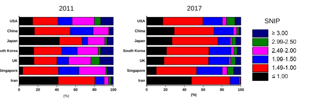
2.3.1 Scientific papers
Figure 2-2a shows share distributions of scientific papers published in 2004, 2010, and 2017 in the field of 2D materials research. In 2004, USA published the largest number of papers, which occupied about one-quarter of the all publications (22 %), followed by Japan (14 %) and China (10 %). However, in 2004, the most of publications reported graphene-related works and other 2D materials, such as TMCs and h-BN are very few. In 2010 when A. K. Geim and K. S. Novoselov won Nobel Prize in Physics for the first report of graphene, publications from China has rapidly increased and exceeded that from Japan as compared with the share in 2004. Moreover, China became the country that publishes the largest number of scientific papers with almost one third of the all publications in 2017. This significant increase implies that China is intensively investing in the field of 2D materials research. Furthermore, South Korea, Singapore, Spain, and Iran are newly ranked in top 10 during 2010-2017. This also suggests that these countries started to pay a lot of attention to this research field. On the other hand, the shares of USA, Japan, Germany, France, and Italy have gradually declined. Figure 2-2b shows the annual trend of publication share. Significant increase of publications in China from 2008 to 2013 is clearly seen in this graph, while the decrease of the USA is also apparent. It is noted that the share of China exceeds that of USA in 2011. The above