INVITED PAPER
Special Section on Electronic DisplaysApplication of Microwave Photoconductivity Decay Method to Characterization of Amorphous In-Ga-Zn-O Films
Satoshi YASUNO†,††a), Takashi KITA††, Shinya MORITA†††, Aya HINO†††, Kazushi HAYASHI†††, Toshihiro KUGIMIYA†††,andShingo SUMIE†,Nonmembers
SUMMARY Microwave photoconductivity decay (μ-PCD) method was applied to evaluate the effects of chemical composition and Ar+plasma induced damage on the bulk and the surface states in amorphous In-Ga-Zn- O (a-IGZO) films. It was found that the peak reflectivity signal in the pho- toconductivity response increased with decreasing the Ga content, and had a strong correlation with the a-IGZO transistor performances. In addition, the peak reflectivity signals obtained after various Ar+plasma treatment duration were well correlated with the transistor characteristics. With Ar+ plasma treatment, the peak reflectivity signal decreased in accordance with degradation of transistor characteristics. Theμ-PCD method was found to be a very useful tool not only to evaluate the bulk and the surface states, but also to predict the performance of a-IGZO transistors subjected to various plasma processes in the production.
key words: microwave photoconductivity decay, a-IGZO, oxide semicon- ductor, photoconductivity response
1. Introduction
Amorphous In-Ga-Zn-O (a-IGZO) is attracting considerable attention as it could be high-performance channel material in thin film transistors (TFTs) for next generation displays [1]–[5]. The control and monitor of the channel composi- tion, the surface states and the interface states between the protect and the channel layer is of importance because the channel composition directly influences to the TFT perfor- mance [6]–[8], and the surface and the interface states are often created by various manufacturing processes such as plasma process [9], [10]. Microwave photoconductivity de- cay (μ-PCD) method is known as a non-destructive and con- tactless technique and widely used for process control and characterization of defects in various semiconductors [11]–
[15]. In the previous study, for a-IGZO films, we found that the peak reflectivity signals of the photoconductivity responses measured byμ-PCD were governed by the film quality (bulk states) that affects the a-IGZO transistor per- formance [16]. In the present study, we carried outμ-PCD measurements to evaluate the bulk states of a-IGZO films with various Ga contents. In addition, we applied theμ- PCD measurements to evaluate the effect of Ar+plasma in-
Manuscript received February 28, 2012.
Manuscript revised June 8, 2012.
†The authors are with Kobelco Research Institute, Inc., Kobe- shi, 651-2271 Japan.
††The authors are with Kobe University, Kobe-shi, 657-8501 Japan.
†††The authors are with KOBE STEEL, LTD., Kobe-shi, 651- 2271 Japan.
a) E-mail: [email protected] DOI: 10.1587/transele.E95.C.1724
duced damage to the surface states of a-IGZO films and the influence of the SiOx passivation process. We discuss the correlation between the peak reflectivity signals of photo- conductivity responses and transistor performances in terms of chemical composition and the surface states.
2. Experimental
Theμ-PCD measurements were carried out using a commer- cially available lifetime measurement system (KOBELCO Research Institute, LTA-1820SP). To obtain a sufficient signal-to-noise ratio, the differential μ-PCD technique for microwave detection was used [15]. In this system, ex- cess carriers are generated by a laser irradiation to increase the conductivity, resulting in a change in the microwave re- flectivity of the specimen. The change in the reflected mi- crowave power is directly related to the change in the ex- cess carrier density [11], [12], [15]. A semiconductor laser- pumped third harmonic yttrium lithium fluoride (YLF) pulse laser was used for the carrier generation. The wavelength was 349 nm (3.55 eV), and the pulse width was 15 ns. The energy of the exciting light was 3.55 eV and higher than the band gap energy of the a-IGZO film (approximately 3.2 eV) [17], [18]. The penetration depth of the laser light was esti- mated to be approximately 300 nm. The photon flux of the laser pulse was 1×1015cm−2. The microwaves (26 GHz) were guided to both the signal and the reference waveg- uides, and then irradiated on the specimen. The reflected microwaves passed through the waveguides to the detector, and the reflectivity differences between the irradiated and non-irradiated (reference) areas were measured.
The X-ray photoelectron spectroscopy (XPS) measure- ments were applied to investigate the electronic structure in a-IGZO films. A Physical Electronics PHI Quantera SXM with a monochromatic Al Kα source (energy 1486.7 eV) was used. The energy calibration was performed by set- ting the binding energy (BE) of the Au 4f7/2=84.0 eV, Cu 2p3/2=932.7 eV and Ag 3d5/2=368.3 eV. The measurement was carried out at room temperature. The analysis area was 100μm in diameter. The emitted photoelectrons were de- tected at a take-offangle of 30◦.
Figure 1 shows a schematic illustration of the cross- sectional structure of an a-IGZO TFT with a bottom gate structure. An n-type crystalline Si wafer with a 200-nm thick thermally-grown SiO2layer was used as the gate elec- trode and the gate insulator, respectively. The a-IGZO Copyright c2012 The Institute of Electronics, Information and Communication Engineers
Fig. 1 Cross-sectional schematic of the bottom-gate a-IGZO TFT device structure used in this study (W/L=10/200μm).
films with a thickness of 50 nm were then deposited by co- sputtering of Ga2O3, In2O3and ZnO targets at room temper- ature. Three samples were prepared. The compositions of the films confirmed by XPS measurements were In:Ga:Zn= 1:0.7:1, 1:1:1, and 1:2:1, respectively. The input power was controlled in order to obtain the intended chemical compo- sition, while the process pressure of a mixtured Ar and O2
gases was fixed at 5 mTorr. For the evaluation of the ef- fect of Ar+plasma induced damage and the influence of the SiOx passivation process, a-IGZO film with a thickness of 50 nm was deposited by DC sputtering using an InGaZnO4
target. The input power was 200 W and the process pressure of a mixtured Ar and O2 gases was 1 mTorr. The a-IGZO films were photolithographically pattered, and the specimen was annealed at 350◦C for 1 h in air. The Mo source and drain electrodes were then deposited at room temperature by shadow-mask sputtering. The channel length (L) and width (W) were 10μm and 200μm, respectively. For the evaluation of the effect of Ar+plasma induced damage, Ar+ plasma treatments were carried out under the following con- ditions: RF power of 50 W, process pressure of 0.8 Torr at room temperature. The transfer curves were measured us- ing a semiconductor parameter analyzer (Keithley 4200) at room temperature under dark condition.
The a-IGZO films forμ-PCD and XPS measurements were deposited on glass substrates and n-type crystalline Si wafers, respectively. The deposition was done either by co- sputtering of 3 targets or DC sputtering using an InGaZnO4
as mentioned above. The thickness of the film was 50 nm or 100 nm. Then, the films were annealed and treated with Ar+ plasma under the same condition described above.
3. Result and Discussion
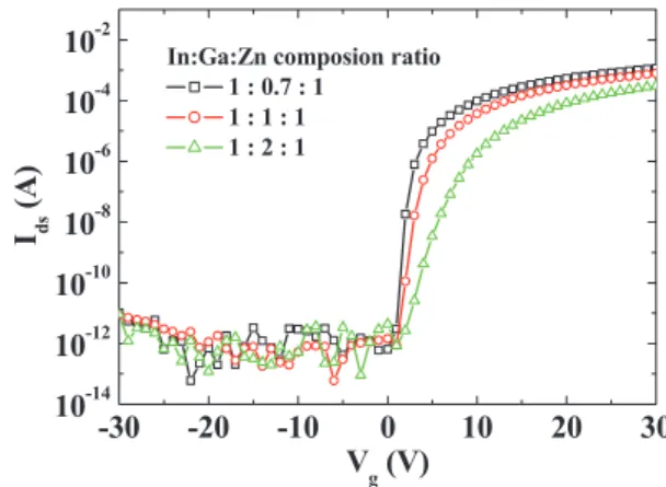
3.1 Evaluation of Bulk States as a Function of Ga Content Figure 2 shows the transfer curves of IGZO TFTs with var- ious Ga contents. Table 1 summarizes the transistor per- formances. The saturation mobilities (μSAT) were extracted from IDS = μSAT (WCOX/2L) (VGS −Vth)2, where IDS is the drain-source current,VGSis the gate-source voltage, and COXis the gate insulator capacitance per unit area. The a- IGZO TFT with the lowest Ga content showed the highest driving current andμSATand the lowest (best) sub-threshold swing (S S) values. The similar compositional dependence has been reported in the literatures [6]–[8], where the same trend was found thatμSATincreased with decreasing Ga con- tent.
Fig. 2 Transfer curves of a-IGZO TFTs atVds =10 V as a function of Ga contents.
Table 1 Performance of a-IGZO TFTs with various Ga contents.
Fig. 3 Photoconductivity response for a-IGZO films as a function of Ga contents. The film thickness of a-IGZO films was 100 nm. The inset depicts a magnified view of the peak signal region.
Figure 3 shows the photoconductivity responses of a- IGZO films with various Ga contents. Each film exhibited a non-exponential decay profile containing a slow decay com- ponent. It can be seen that the peak reflectivity signals in- crease with decreasing the Ga content. On the other hand, the slope of the slow decay hardly varies with the Ga con- tents. We infer that the slow decay is related with the trap- ping processes by defects and/or by other factors. In the pre- vious study, we evaluated theμ-PCD mapping over a wide compositional space of a- IGZO film deposited on a 6-inch glass substrate by co-sputtering of 3 targets [16]. In the map of the peak reflectivity signal, the same tendency depending on the Ga content was observed.
Figure 4 plots the values ofμSATagainst the peak reflec- tivity signals. The peak reflectivity signals become higher withμSAT, and the linear relationship betweenμSATand the
Fig. 4 Peak reflectivity signal for a-IGZO films as a function of saturation mobility.
peak signals is clearly seen. This is consistent with pre- vious report showing that the peak reflectivity signal has a strong correlation withμSAT, and implies that the peak re- flectivity signal directly corresponds to the density of the sub-gap states of a-IGZO bulk region [16]. Also, it has been reported that Zn contributes to the modulation of the shallow tail states below the conduction band [6]. It is reasonable to suppose that the sub-threshold characteristics were im- proved with decreasing the Ga content and/or increasing the Zn content. In addition, electron mobility strongly depends on the carrier concentration [2]. The carrier concentration of the present films are around 1018cm−3and increases with decreasing Ga content. Within the present carrier concen- tration range, the number of effective recombination and/or trapping centers decreases with increasing carrier concen- tration as a result of the Fermi level shift toward the conduc- tion band minimum. This leads to an increase in the satu- ration mobility. Therefore, we infer that the density of the sub-gap states, including the tail states, that act as trapping and/or recombination centers, is lower with decreasing the Ga content. Hence, in the present study, the a-IGZO film with low Ga content exhibited more photo-generated carri- ers survived during the laser pulse illumination, that leads to higher peak reflectivity signal, compared to that with high Ga content.
3.2 Evaluation of Surface and Interface States 3.2.1 Ar+Plasma Induced Damage
Figure 5 shows the transfer curves of a-IGZO TFTs as a function of Ar+plasma treatment duration. As shown in the figure, the untreated (0 s) TFT shows good transfer curve.
μSATwas found to be 8.3 cm2/Vs and S S was 0.33 V/dec.
On the other hand, most TFTs with the Ar+ plasma treat- ment show a drastic increase in the off-current. Conducting behaviors with no turn-offis also observed already for the 3 s plasma treatment. It has been reported that the plasma treatment creates oxygen deficiency for the metal oxide ma- terials, resulting in an increase in electron carriers on the surface region [19], [20].
Fig. 5 Transfer curves of a-IGZO TFTs atVds =10 V as a function of Ar+plasma treatment duration. The inset shows peak reflectivity signals for a-IGZO films as a function of Ar+plasma treatment time.
Fig. 6 Valence band spectra for a-IGZO films as a function of Ar+ plasma treatment duration. The inset depicts enlarged spectra showing va- lence band edge region.
The inset of Fig. 5 shows the peak reflectivity signals of photoconductivity responses as a function of Ar+plasma treatment duration. The peak reflectivity signals became lower with increasing the treatment duration. It is clear that the peak reflectivity signal have a strong correlation with the Ar+plasma treatment duration. This result indicates that the peak reflectivity signal strongly reflects surface state, since the bulk state is hardly influenced by the plasma treatment.
Considering this result and the previous report [16], it is sug- gested that the peak reflectivity signal consists with not only the bulk states but also surface states. It is reasonably as- sumed that the peak reflectivity signal is attributed to the recombination and/or trapping processes that originated in bulk and surface states. Therefore, the peak reflectivity sig- nal decreased due to the increasing the surface states caused by Ar+plasma treatment.
XPS analysis was carried out in order to investigate the surface electronic structure of a-IGZO films with Ar+ plasma treatment. Figure 6 shows the valence band (VB) spectra of a-IGZO films with various Ar+plasma treatment duration. The VB of a-IGZO consists mainly of O 2p and Zn 3d states. The VB edge was defined as the point where the linear extrapolation along the lower BE side of O 2p (around
4–5 eV) intersects the baseline. The values of the VB edge are 3.8 eV and 3.4 eV for a-IGZO films with and without 300 sec Ar+plasma treatment, respectively. Similar energy shifts were also observed in Zn 3d, O 1s, In 4d and Ga 2p (the spectra of O 1s and Ga 2p are not shown) depending on the Ar+plasma treatment duration. It is likely that this ob- servation correlates with Fermi level shift [21]–[23] rather than the charging up effect. Min et al. have reported that Fermi level shifts by oxygen deficiency in the ZnO films [21]. In our study, the films exposed to Ar+plasma showed conducting behavior as shown in Fig. 5. Thus, it is inferred that the Fermi level approaches to the conduction band (CB) edge. As the Fermi level shifts closer to the CB edge, the conduction electrons increase due to thermal excitations.
Hence, we suggest that the BE shift with Ar+plasma treat- ment is mainly due to the Fermi level shift. In particular, it is likely to consider that the Fermi level of the a-IGZO for the 300 s Ar+plasma treatment is located at the CB level, so that transport mechanism is nearly metallic. The inset of Fig. 6 shows enlarged VB edge of the a-IGZO films with various Ar+ plasma treatment duration. As shown in the figure, the intensity near BE∼6 eV decreases with the Ar+ plasma treatment, indicating an increasing of the oxygen de- ficiency by exposing to Ar+plasma [24].
3.2.2 Effects of SiO2Passivation
To confirm that the peak reflectivity signal reflects the sur- face states as well as the bulk states, we investigated the influence of SiO2 passivation layer on a-IGZO film for the photoconductivity response. It has been reported that the characteristics of TFTs are influenced by plasma-enhanced chemical vapor deposition (PECVD) process depending on the process conditions. Therefore, for passivation of the a- IGZO film, SiO2layer was deposited by PECVD at 150◦C on the a-IGZO film since the low temperature (∼150◦C) PECVD of SiO2 passivation layers suppress the surface states at the back channel and improved TFT characteris- tics [25]. The thickness of the SiO2layer was 50 nm. Fig- ure 7 shows the photoconductivity responses of a-IGZO films with and without SiO2 passivation layer. It can be
Fig. 7 Photoconductivity response for a-IGZO films with and without SiO2passivation layer. The film thickness of a-IGZO films were 100 nm.
seen that the a-IGZO film with the SiO2passivation layer ex- hibits higher peak reflectivity signal compared to that with- out the SiO2 passivation layer. It is inferred that the op- timized SiO2 passivation layer decreases the surface states of a-IGZO film, that leads to more photo-generated carri- ers survived during the laser pulse illumination. This result supports the mechanism proposed above that the peak re- flectivity signal consists with the bulk states and the surface states. Therefore, contrary to the Ar+plasma irradiation, it was observed that the peak reflectivity signal of the a-IGZO with the SiO2passivation layer was increased due to the re- duction of the surface states.
4. Conclusion
We investigated the μ-PCD measurements to evaluate the a-IGZO films as functions of the chemical composition and the Ar+plasma treatment duration. The peak reflectivity sig- nal increased with decreasing the Ga content in the film, and the correlation was confirmed between the peak reflectivity signals and the transistor performances of the a-IGZO TFTs.
It is suggested that the peak reflectivity signal directly corre- sponds to the density of sub-gap states of a-IGZO bulk film.
In addition, it was found that the peak reflectivity signal de- creased with the Ar+ plasma treatment due to the increase of the surface states caused by the defects such as oxygen deficiency. On the other hand, the peak reflectivity signal in- creased due to the reduction of the surface states originating from the SiO2passivation layer. Hence, it is concluded that the peak reflectivity signal is strongly affected by the surface states as well as the bulk states. μ-PCD measurement is re- ally effective to characterize the compositional dependence and the effect of the plasma process of a-IGZO films in re- search and development stage and expected to apply to the process control and management in both in-line and off-line inspection tools.
Acknowledgments
The authors thank Dr. S. Takahashi for useful discussion on XPS results.
References
[1] K. Nomura, H. Ohta, A. Takagi, T. Kamiya, M. Hirao, and H.
Hosono, “Room-temperature fabrication of transparent flexible thin- film transistors using amorphous oxide semiconductors,” Nature, vol.432, pp.488–492, 2004.
[2] K. Nomura, A. Takagi, T. Kamiya, H. Ohta, M. Hirano, and H.
Hosono, “Amorphous oxide semiconductors for high-performance flexible thin-film transistors,” Jpn. J. Appl. Phys., vol.45, pp.4303–
4308, 2006.
[3] H. Yabuta, M. Sano, K. Abe, T. Aiba, T. Den, H. Kumoni, K.
Nomura, T. Kamiya, and H. Hosono, “High-mobility thin-film tran- sistor with amorphous InGaZnO4channel fabricated by room tem- perature rf-magnetron sputtering,” Appl. Phys. Lett., vol.89, 112123, 2006.
[4] J.K. Jeong, J.H. Jeong, H.W. Yang, J.-S. Park, Y.-G. Mo, and H.D.
Kim, “High performance thin film transistors with cosputtered amor- phous indium gallium zinc oxide channel,” Appl. Phys. Lett., vol.91,
113505, 2007.
[5] K. Nomura, T. Kamiya, H. Ohta, M. Hirano, and H. Hosono, “De- fect passivation and homogenization of amorphous oxide thin-film transistor by wet O2annealing,” Appl. Phys. Lett., vol.93, 192107, 2009.
[6] T. Iwawsaki, N. Itagaki, T. Den, H. Kumomi, K. Nomura, T.
Kamiya, and H. Hosono, “Combinatorial approach to thin-film tran- sistors using multicomponent semiconductor channels: An appli- cation to amorphous oxide semiconductors in In-Ga-Zn-O system,”
Appl. Phys. Lett., vol.90, 242114, 2007.
[7] J.Y. Huh, J.H. Jeon, H.H. Choe, K.W. Lee, J.H. Seo, M.K. Ryu, S.H.K. Park, C.S. Hwang, and W.S. Cheong, “Effects of the com- position of sputtering target on the stability of InGaZnO thin film transistor,” Thin Solid Films, vol.519, 6868, 2011.
[8] D. Kim, C.Y. Koo, K. Song, Y. Jeong, and J. Moon, “Compositional influence on sol-gel-derived amorphous oxide semiconductor thin film transistors,” Appl. Phys. Lett., vol.95, 103501, 2009.
[9] J. Park, S. Kim, C. Kim, S. Kim, I. Song, H. Yin, K.K. Kim, S. Lee, K. Hong, J. Lee, J. Jung, E. Lee, K.W. Kwon, and Y. Park, “High- performance amorphous gallium indium zinc oxide thin-film tran- sistors through N2O plasma passivation,” Appl. Phys. Lett., vol.93, 053505, 2008.
[10] M.J. Lee, S.J. Kang, J.Y. Baik, K.J. Kim, H.D. Kim, H.J. Shin, J.
Chung, E. Lee, J. Lee, and J. Lee, “Sputtering effect on amorphous Ga-In-Zn-O thin-film surface: Occurrence of subgap and metallic states,” Electrochem. Solid-State Lett., vol.13, H454, 2010.
[11] K. Kunst and G. Beck, “The study of charge carrier kinetics in semi- conductors by microwave conductivity measurements. II.,” J. Appl.
Phys., vol.63, pp.1093–1098, 1988.
[12] K. Kunst and G. Beck, “The study of charge carrier kinetics in semiconductors by microwave conductivity measurements,” J. Appl.
Phys., vol.60, pp.3558–3566, 1986.
[13] J.R. Jenny, D.P. Malta, V.F. Tsvetkov, M.K. Das, H. McD. Hobgood, and C.H. Carter, Jr, “Effects of annealing on carrier lifetime in 4H- SiC,” J. Appl. Phys., vol.100, 113710, 2006.
[14] M. Ichimura, N. Yamada, H. Tajiri, and E. Arai, “Slow photocon- ductivity decay in 3C-SiC on Si substrates,” J. Appl. Phys., vol.84, pp.2727–2731, 1998.
[15] S. Sumie, F. Ojima, K. Yamashita, K. Iba, and H. Hashizume, “Life- time mapping technique for ultrathin silicon-on-insulator wafers,” J.
Electrochem. Soc., vol.152, G99, 2005.
[16] S. Yasuno, T. Kugimiya, S. Morita, A. Miki, F. Ojima and S. Sumie,
“Correlation of photoconductivity response of amorphous In-Ga-Zn- O films with transistor performance using microwave photoconduc- tivity decay method,” Appl. Phys. Lett., vol.98, 102107, 2011.
[17] K. Nomura, T. Kamiya, H. Yanagi, E. Ikenaga, K. Yang, K.
Kobayashi, M. Hirano, and H. Hosono, “Subgap states in trans- parent amorphous oxide semiconductor, In-Ga-Zn-O, observed by bulk sensitive x-ray photoelectron spectroscopy,” Appl. Phys. Lett., vol.92, 202117, 2008.
[18] J.W. Park, P.S. Jeong, S.H. Choi, H. Lee, B.H. Kong, and H.K. Cho,
“Optical and structural properties of ion-implanted InGaZnO thin films studied with spectroscopic ellipsometry and transmission elec- tron microscopy,” Jpn. J. Appl. Phys., vol.48, 111603, 2009.
[19] J.S. Park, J.K. Jeong, Y.G. Mo, and H.D. Kim, “Improvements in the device characteristics of amorphous indium gallium zinc oxide thin- film transistors by Ar plasma treatment,” Appl. Phys. Lett., vol.90, 262106, 2007.
[20] J.S. Kim, F. Cacialli, A. Cola, G. Gigli, and R. Cingolani, “Increase of charge carriers density and reduction of Hall mobilities in oxygen- plasma treated indium-tin-oxide anodes,” Appl. Phys. Lett., vol.75, pp.19–21, 1999.
[21] C.H. Min, S. Cho, S.H. Lee, D.Y. Cho, W.G. Park, J.G. Chung, E.
Lee, J.C. Lee, B. Anass, J.H. Lee, C.S. Hwang, and S.J. Oh, “Effect of oxygen partial pressure on the Fermi level of ZnO1−xfilms fabri- cated by pulsed laser deposition,” Appl. Phys. Lett., vol.96, 201907, 2010.
[22] S.J. Kang, J.Y. Baik, A. Thakur, H.D. Kim, H.J. Shin, J. Chung, J. Lee, and J. Lee, “Surface-chemistry-sensitive spectral features of In-Ga-Zn-O thin film: Cleaned, air-passivated, and sputter-phase- separated surfaces,” Chem. Phys. Lett., vol.510, pp.234–236, 2011.
[23] K. Nomura, T. Kamiya, E. Ikenaga, H. Yanagi, K. Kobayashi, and H.
Hosono, “Depth analysis of subgap electronic states in amorphous oxide semiconductor, a-In-Ga-Zn-O, studied by hard x-ray photo- electron spectroscopy,” J. Appl. Phys., vol.109, 073726, 2011.
[24] D.Y. Cho, J.H. Kim, U.K. Kim, Y.J. Chung, J. Song, C.S. Hwang, J.M. Lee, and S.J. Oh, “Spectroscopic investigation on the origin of photoinduced carrier generation in semiconducting InGaO and InGaZnO films,” J. Phys. Chem. C, vol.114, 11962, 2010.
[25] S.H. Choi and M.K. Han, “Effect of deposition temperature of SiOx passivation layer on the electrical performance of a-IGZO TFTs,”
IEEE Electron Device Lett., vol.33, no.3, pp.396–398, 2012.
Satoshi Yasuno received the B.Eng.
and M.Eng. degrees in applied chemistry from Gifu University in 2001 and 2003 respec- tively. In 2003, he joined Kobelco Research Institute, Inc., Kobe, Japan, and has been working on physical analysis particularly with high-resolution Rutherford back scattering spec- troscopy. Since 2009 joined a project for oxide semiconductor for FPD in Electronics Research Lab. in Kobe steel, LTD., he has characterized physical property of oxide semiconductor and developed evaluation method for film quality of oxide semiconductor with Microwave photoconductivity decay. Currently he is at Kobelco Research Institute, Inc. and Kobe university.
Takashi Kita is professor of electrical and electronic engineering of Kobe University, where he works on epitaxial growth and ma- terial physics of III–V material-based quan- tum heterostructures and semiconductor nanos- tructures for optical amplifier, ultra-fast optical switch, new generation solar cells, and novel light sources. He received the Ph.D. Degree in electrical engineering from Osaka Univer- sity, Osaka, Japan, in 1991. Contact him at [email protected].
Shinya Morita received the B.Sci. and M.Sci. degrees in physics from Hiroshima Uni- versity in 2005 and 2007 respectively. Since he joined Kobe Steel, LTD., Kobe Japan in 2007, he has extensively explored new metal film ma- terials for interconnection of FPD. He has in- volved himself in the studies on development new oxide materials and fabrication processes of oxide TFTs for FPD. He received the Outstand- ing Poster Paper Award of IDW in 2010 for re- search of Oxide semiconductor materials.
Aya Hino received the B.Sci. and M.Sci. de- grees in physics from Tohoku University in 2003 and 2005, respectively. Since she joined Kobe Steel, LTD., Kobe, Japan in 2005, she has ex- tensively explored new alloy films for intercon- nection for FPD. Since 2009 when she joined a project for oxide TFTs for FPD, she has ex- plored characteristics of oxide TFTs.
Kazushi Hayashi received the Master’s de- gree from Osaka University, Japan, in 1992, and joined Kobe Steel, Japan. He was awarded the Doctor’s degree from Osaka University in 1997.
Since he joined Kobe Steel, he has engaged in the research and development of semiconduct- ing materials and devices. His research interest in an oxide TFTs project is electronic properties of amorphous oxide semiconductors.
Toshihiro Kugimiya received the B.S., M.S. and Dr. degrees in electronics engineer- ing from Toyohashi University of Technology in 1991, 1993, and 2011, respectively. In 1993, he joined KOBE STEEL, LTD., Japan, and he has worked on metal interconnections for FPD, es- pecially, Al-alloy film interconnections. Since 2009 when he joined a project for OXIDE semi- conductor for FPD in Electronics Research Lab.
in KOBE STEEL, he has directed the research of OXIDE-TFT fabrication process and analy- ses of OXIDE materials and TFTs.
Shingo Sumie received Dr. degrees in en- gineering from Osaka Prefecture University in 1995. In 1989, he joined Kobe Steel, LTD., Kobe, Japan and researched on several physi- cal analysis methods using optical technology.
From 2001, he works in Kobelco Research In- stitute, Inc., Kobe, Japan and continues to de- velop the evaluation system for LSI semicon- ductor wafer, FPD poly-Silicon and oxide semi- conductor films using Microwave photoconduc- tivity decay technique.