INVITED PAPER
Special Section on Recent Advances in Integrated Photonic DevicesIntegrated Photonic Platforms for Telecommunications: InP and Si
Christopher R. DOERR†∗a),Nonmember
SUMMARY There is a relentless push for cost and size reduction in optical transmitters and receivers for fiber-optic links. Monolithically inte- grated optical chips in InP and Si may be a way to leap ahead of this trend.
We discuss uses of integration technology to accomplish various telecom- munications functions.
key words: advanced modulation formats, coherent, fiber optic commu- nication, gratings, indium phosphide, photonic integrated circuits, silicon photonics
1. Introduction
The first fiber-optic transmitters simply modulated the power of a laser. High power represented a digital 1 and low power represented a digital 0. The first fiber-optic receivers consisted of a single photodetector and transimpedance am- plifier, converting the optical power to a voltage. This trans- mission format is called on-offkeying (OOK). OOK is sim- ple to implement, but the spectral efficiency is at best 1, i.e., it requires at least 1 Hz of spectrum to transmit 1 bit/s, and the electronics speed must be at least∼0.7 times the bit rate.
There are more complex modulation formats that increase the spectral efficiency and reduce the electronics speed. For example, by employing dual-polarization quadrature phase- shift keying (DP-QPSK), the spectral efficiency is increased to 4, and the electronics speed is reduced to∼0.18 times the bit rate. However, creating and receiving DP-QPSK requires a highly complex transmitter and receiver with∼38 optical and electro-optical components. Such transceivers are an ideal application for photonic integrated circuits (PICs).
We focus here on semiconductor PICs. Semiconduc- tor PICs have compact optoelectronic components. The two main material systems for semiconductor PICs are the group III-V materials and the group IV materials, as shown in Fig. 1. The group III-V family is shown in Fig. 2 and con- sists mainly of In, P, Ga, As, and Al. The group IV family is shown in Fig. 3 and consists mainly of Si, Ge, O, and N.
The group III-V material system has a direct band gap, allowing it to have efficient lasers, and it can have ternary or quaternary compounds, allowing for a rich set of material properties. The group IV material system has much more easily obtained materials (27% of the mass of the Earth’s
Manuscript received November 29, 2012.
Manuscript revised February 25, 2013.
†The author was with Alcatel-Lucent, Bell Laboratories, Holmdel, NJ, USA.
∗Presently, with Acacia Communications, Middletown, NJ, USA.
a) E-mail: [email protected] DOI: 10.1587/transele.E96.C.950
Fig. 1 Typical group III-V (a) and group IV (b) waveguides.
Fig. 2 The Group III-V InP family of integrated optic materials.
Fig. 3 The Group IV family of integrated optic materials.
crust is Si, whereas only 0.000005% is In) and can be eas- ily oxidized into a very high quality material, SiO2. The oxide allows for facile wafer bonding, which in turn allows for the creation of high-index-contrast waveguides without any epitaxy, resulting in extremely high yield. Group IV materials integrate well with high-index dielectric materi- als, such as Si3N4and SiON. Very roughly speaking, group III-V materials are strongest in optoelectronic devices that require optical gain, and group IV materials are strongest in optoelectronic devices that require special characteristics such as polarization splitting/combining, very compact size, and very high yield. Of course, there are many exceptions.
Copyright c2013 The Institute of Electronics, Information and Communication Engineers
This paper will discuss various semiconductor PICs for use in advanced optical communications systems.
2. Fiber Coupling
We first discuss coupling of optical fiber to PICs.
2.1 Single-Mode Fiber Coupling
There are two main approaches to coupling a single-mode fiber to a PIC. The first is facet coupling, in which the fiber is parallel to the plane of the PIC. In this case, the waveguide mode in the PIC must be expanded both horizontally and vertically.
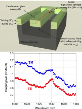
A powerful structure for facet coupling with group IV materials is the cantilever adiabatic coupler shown in Fig. 4 [1]. The Si or, in this case, Si3N4waveguide is tapered lat- erally to as small a tip as possible and as slowly as possible.
The effective index of the fundamental mode will decrease and approach that of the surrounding oxide. This will cou- ple with high efficiency to a waveguide made of the oxide with etched walls and undercut underneath and filled with a material with an index lower than that of the cladding. Such a structure can achieve of coupling loss to cleaved standard single mode fiber of less than 1.2 dB and 2.0 dB to Si3N4
and Si waveguides, respectively, over a broad bandwidth.
A powerful structure for vertical coupling is the grating coupler [2], [3]. It is a first-order grating with a period ap- proximately equal to the wavelength in the material. Com- paring a grating coupler to a facet coupler, the facet coupler usually has lower loss, wider bandwidth, and higher return loss; and the grating coupler can be used for on-wafer test- ing, can serve naturally as a polarization splitter and rotator,
Fig. 4 Si3N4cantilever spot-size converter.
and does not need small Si/Si3N4tips and fragile cantilever structures.
A grating coupler needs a high vertical index contrast, otherwise the grating cannot be made strong enough without causing the effective index of the mode to fall below that of the cladding when the grooves are put into the waveguide.
This is a case where Si waveguides have a significant ad- vantage because they are created using wafer bonding and thus have oxide above and below. InGaAsP waveguides, on the other hand, are usually formed by epitaxy and have InP below. Thus to make a grating coupler in III-V materials, one must suspend the waveguide, or something similar, by etching underneath the waveguide [4].
The 1-dB bandwidth of a grating coupler is approxi- mately
Δλ1 dB=
2 ln(10)
5 NA λ0cosθ0
nw−n0sinθ0 (1) where NA is the fiber numerical aperture, λ0 is the free- space center wavelength,θ0 is the angle of incidence,n0 is the cladding index, andnwis the effective index in the grat- ing [5]. The grating coupler bandwidth can be increased by using a lowernw. One way to do this is to make the grating in Si3N4, which has an index of 2.0, instead of Si, which has an index of 3.7. Figure 5 shows a 400-nm-thick Si3N4 grating coupler with a 67-nm 1-dB bandwidth [5].
Grating couplers require a thin, high-index-contrast slab waveguide, and thus the birefringence is generally very high. Thus the grating coupler can usually be designed to couple either transverse-electric (TE) or transverse- magnetic (TM) polarization, but not both at the same wave- length and in the same direction. In fact, this is key to the operation of polarization-splitting grating couplers [6].
However, one can make the grating coupler polariza- tion independent by using a sub-wavelength structure. The basic concept is based on the fact that allEandHfield com- ponents are continuous across a non-magnetic boundary ex- cept for theE field component normal to the boundary. In that case, it is E that is continuous. This is why a thin slab waveguide has a higher effective index for TE polar- ized light than TM: the TM polarized light has strong E field components normal to the top and bottom surfaces and thus pushes out into the cladding, where is small, above and below the waveguide much more than TE polarized light, in order to make E constant across the boundary. In the sub-wavelength structure, one removes sections laterally to
Fig. 5 Si3N4grating coupler.
Fig. 6 Polarization-independent grating coupler design.
make the TE-polarized light push out sideways into the in- tervening cladding, equalizing the effective indices for TE and TM. Such a design was proposed in [7]. However, [7]
uses holes to create the sub-wavelength structure.
One can use pillars instead [8]. This should have im- proved performance because the holes case can be viewed as an alternating series, along the propagation direction, of solid slab waveguide and sub-wavelength-fractured slab waveguide, whereas the pillars case can be viewed as an alternating series of no waveguide and sub-wavelength- fractured slab waveguide. The fractured waveguide is de- signed to have zero birefringence. However a solid slab waveguide has high birefringence, whereas an empty wave- guide has zero birefringence. Thus the polarization depen- dence of the pillar case is lower since both parts of each pe- riod, the empty waveguide and the fractured slab waveguide, are each polarization independent. In [7] a polarization- independent wavelength for the grating was simulated, but the TE diffraction strength was significantly stronger than for TM because the high birefringence of the solid slab waveguide section must be compensated by the fractured slab waveguide section.
Our design is shown in Fig. 6. It is a U-shaped struc- ture with grating couplers at each end. The waveguide is Si and is 220 nm thick. The etching is completely through the waveguide, creating an array of pillars of Si. The entire structure is buried in oxide. The lithography was done using direct e-beam writing.
The measured results of the polarization-independent grating coupler are shown in Fig. 7, showing the maximum and minimum response over all polarizations. As one can see, the polarization dependent loss is less than 1 dB over the C-band. The bandwidth is also very wide, because of the low effective index of the sub wavelength structure. Un- fortunately, the insertion loss is high, 12–13 dB per grating coupler. It is not currently understood why the loss is so high and whether this is due to the grating coupler itself or loss in the waveguide.
Fig. 7 Measured coupling efficiency of sub-wavelength-structured 1-D grating coupler showing maximum (red) and minimum (blue) over all po- larizations.
Fig. 8 Photograph of the cross section of a 7-core fiber.
2.2 Multicore Fiber Coupling
Deployed fibers today have only one core. The cross section of a new 7-core multicore fiber (MCF) is shown in Fig. 8 [9].
An MCF increases the spatial connection density. It would be difficult to make a facet coupler that couples a PIC to all seven cores. However, grating coupling is well-suited for matching a 2-D arrangement of cores.
Figure 9 shows a 7-core receiver PIC in silicon. It con- tains seven 1-D grating couplers arranged to match the fiber cores, with the fiber tilted 10◦to the right. These 1-D grating couplers are conventional and thus have a high polarization dependence. To receive both polarizations, the fiber tilt was chosen such that TE light coupled to one direction and TM light coupled to the other [10]. The PIC contains length- imbalanced MZIs, serving as two-channel wavelength de- multiplexers. Thus this chip exhibits space, wavelength, and polarization diversity.
2.3 Multimode Fiber Coupling
Another new type of fiber being explored for tomorrow’s networks is a few-mode fiber (FMF). An FMF is a multi- mode fiber that guides ∼10 modes. In contrast, a typi-
Fig. 9 7-core fiber receiver PIC in Si. (a) photograph of the PIC and (b) waveguide layout.
Fig. 10 Calculated modes of a 5-mode (10 modes if include polarization) ring-core fiber.
Fig. 11 Multimode ring-core fiber coupler silicon PIC.
cal multi-mode fiber used in short-reach connections guides 100 s of modes.
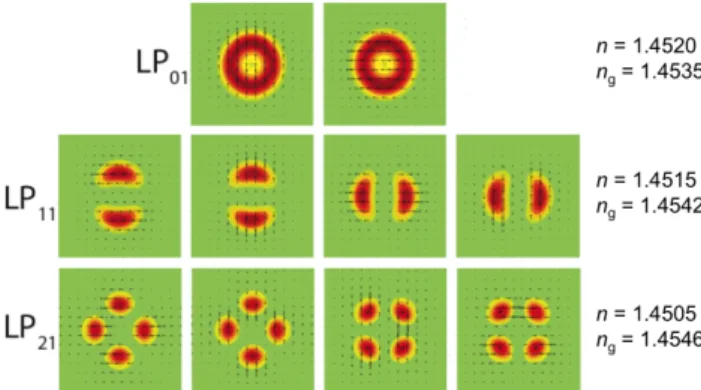
There are many designs for FMFs. An FMF with a ring-shaped core can be designed to be multi-mode az- imuthally but single-mode radially. Such a fiber is well suited for coupling to the top surface of a PIC, because it allows all the modes to be accessed via a planar geometry without requiring waveguide crossings. The calculated fiber modes of a 10-mode ring-core fiber are shown in Fig. 10.
A PIC for coupling to a ring-core FMF is shown in Fig. 11 [11]. It consists of a circular grating coupler [12] connected
Fig. 12 Physical configuration mapping of angular momentum modes to ring-core fiber modes.
Fig. 13 Configuration for optical MIMO demultiplexing. The solid rect- angles are power splitters, the rectangles containing infinity signs are infi- nite phase shifters, and the switches are adjustable power combiners.
with equal-length waveguides to a star coupler. Each port of the star coupler couples to a different optical angular mo- mentum state at the circular grating coupler, e.g. the cen- ter star coupler port couples to the grating coupler mode in which all the waveguides are in phase, giving an angular momentum of zero. The adjacent star coupler port excites a mode with a 2πlinear phase change around the ring, result- ing in an angular momentum mode of±1. The angular mo- mentum modes are linear combinations of the ring-core fiber modes, as shown in Fig. 12. This particular device works for only one polarization, due to the strong polarization- dependence of the grating coupler. This could be solved by using a lateral sub-wavelength structure, as described in Sect. 2.1.
If there is coupling between the modes in the FMF, then when the light is received, each mode will contain a linear combination of all the launched signals. Because the signals will remain essentially orthogonal, then the original signals can be recovered by adding together a linear combination of the fields in each mode. This addition is typically done in a digital signal processor (DSP) [13]. However, such a DSP may consume very high power. One can instead perform the demultiplexing optically [14], saving significant power consumption, provided that the modal dispersion is low. An architecture for separating out intermixed modes, i.e. opti- cal multiple-input multiple-output (MIMO) demultiplexing, is shown in Fig. 13(a), and an experimental demonstration that demultiplexes one mode from six modes is shown in Fig. 13(b) [15]. In Fig. 13(a) there areNinputs on the left- hand side consisting each of a linear combination ofNorig- inal optical signals. This linear combining occurred during transmission in e.g. a multi-mode fiber. The N inputs are each splitNways byNpower splitters. There are control- lable phase shifters, which must have infinite range, onN−1
of the outputs of each power splitter and these control the relative phases between the signals as they interfere inside the adjustable power combiners. By choosing the proper rel- ative phases and combining magnitudes, theN outputs on the right-hand side consist of theN original, unmixed sig- nals. The experiment in Fig. 13(b) employed a three-mode fiber (six modes including polarization). Six independent signals were launched into the fiber. After propagation, the six modes in the fiber contain orthogonal linear combina- tions of the original six signals. At the output, three 2-D grating couplers [shown at the left in Fig. 13(b)] collected the six mixed signals. This demonstration demultiplexes only one signal, so there are no power splitters. There are six phase shifters to adjust the relative phases between the six mixed signals. The phase shifters are made endless (i.e., never run out of range) by placing each one inside an inter- ferometer with optical switches on each end. Under normal operation, the optical switches direct to and receive from only the phase shifter. However, when the phase shifter reaches 0 or 4π, the switches temporarily switch the path to the other arm of the interferometer, the phase shifter is re- set to 2π, and the switches switch back to normal operation.
The six signals are interfered with each other via five tun- able couplers in a tree network. There is a tap at the output with an integrated photodiode to use for feedback control.
The feedback signal measures the RF power and attempts to minimize it, for the case when the original signals are phase-shift-keyed.
3. Comb Generation
Single-channel bit rates above ∼200 Gb/s are difficult to achieve with today’s technology. A practical solution is to use multiple optical carriers bundled as a super channel.
One could create the carriers using a plurality of indepen- dent lasers, but this has issues with cost, reliability, power consumption, and yield. Another solution is to use a sin- gle laser but create the multiple carriers using a modulating PIC. An example of such a PIC in III-V materials is shown in Fig. 14 [16]. It employs a resonant structure with a semi- conductor optical amplifier in the feedback path to enhance the comb generation.
Fig. 14 Multicarrier generator in InP.
4. Optical Isolation
Many PICs would benefit from an integrated optical isolator, especially ones that contain optical amplifiers. An optical isolator is a non-reciprocal device. Reciprocity means that the reaction of source A on source B is equal to the reac- tion of source B on source A. This means you need two test sources to see if something is reciprocal or not, and what you measure has to be projected onto the source. In other words, for example, if the two sources are in certain modes, you have to measure the powers in those modes, not the total power. If you do not do this, then a passive, non-magnetic can be incorrectly seen as non-reciprocal [17].
An isolator in InP using two phase modulators is shown in Fig. 15 [18]. It comprises two phase modulators driven with single-frequency signals in quadrature separated by a distanceΔL=vg/(4f), wherevgis the optical group velocity and f is the modulation frequency.
The advantage is it does not require any magneto-optic materials, which can be difficult to integrate and optically lossy. The disadvantages are that the isolation is very narrow band and requires active modulation.
5. Wavelength Demultiplexing
Wavelength-division multiplexing (WDM) is the use of mul- tiple parallel wavelength channels to increase the capacity of a fiber-optic link. To demultiplex more than a couple channels, gratings are usually preferred. The gratings are often arrayed waveguide gratings (AWGs) [19] because of their ease of manufacture. AWGs can be made in semicon- ductor waveguides, such as InP [20]. Figure 16 shows a four-channel coherent receiver made in InP [21]. It uses an interleave-chirped AWG to perform the wavelength demulti- plexing, the polarization demultiplexing, and the 90◦-hybrid operation.
Despite the success of AWGs in semiconductors, it is usually more advantageous to make the AWG in a di- electric material, such as Si3N4. Si3N4 has a lower in-
Fig. 15 Optical isolator in InP.
Fig. 16 Four-channel coherent receiver in InP.
Fig. 17 Eight-channel polarization-independent CWDM receiver in Si and Si3N4waveguides.
Fig. 18 40-channel receiver in Si and Si3N4waveguides.
dex, resulting in lower phase errors, and five times lower temperature dependence than Si or InP. Figures 17 and 18 show a polarization-independent CWDM receiver [22] and a polarization-dependent 40-channel receiver [23], respec- tively, in Si, Si3N4, and Ge materials. For both designs, the Si thickness is 220 nm and the Si3N4 thickness, which is deposited above the Si waveguide, is 400 nm. Coupling between the Si and Si3N4 layers is accomplished via adi- abatic inverse tapers. In both designs the input is a Si3N4
Fig. 19 Si and Ge 100-Gb/s coherent receiver.
Fig. 20 Two possible polarization demultiplexer configurations for use in PICs. Yellow phase shifters are analog whereas green ones are digital.
cantilever facet coupler, as described above; the AWG is in Si3N4, the multi-mode Si3N4 output waveguides transi- tion to multi-mode Si waveguides, and the photodetectors are 850 nm of Ge on top of the Si.
6. Coherent Reception
To receive an advanced modulation format like DP-QPSK, one usually employs coherent detection. Figure 19 shows a dual-polarization, dual-quadrature 100-Gb/s coherent re- ceiver in Si and Ge [24]. It uses two 2-D grating couplers at 0◦incidence to act as fiber couplers and polarization split- ters for the signal and local oscillator. Thermooptic phase shifters are used to set the phases for the two 90◦hybrids.
7. Optical Polarization Demultiplexing
To receive a dual-polarization signal after transmission over standard fiber, one must unscramble the two polarizations.
This is usually done in the DSP of a coherent receiver. How- ever, there may be cases in which one cannot afford the cost and power of a high-speed DSP. In such a case, one can use optical polarization demultiplexing [25]. The simplest PIC optical polarization demultiplexer comprises a polarization beam splitter and rotator (PBSR) and a phase shifter and a tunable coupler. The tunable coupler is a Mach-Zehnder interferometer with a phase shifter in one arm. Thus the to- tal number of controls is two. Unfortunately, such a simple polarization controller is not endless: the first phase shifter may eventually run out of adjustment range and need a re- set as the input polarization is tracked. Two possible op- tical endless polarization demultiplexer configurations suit- able for use in PICs are shown in Fig. 20. They each need four controls.
Fig. 21 DP-DQPSK receiver in Si and Ge.
Fig. 22 Flexible-grid wavelength-selective switch in Si and Si3N4
waveguides.
Figure 21 shows a DP-DQSPK receiver in Si and Ge using the latter type of endless polarization demultiplexer. It could receive a 43-Gb/s DP-DQPSK signal without needing a high-speed DSP [26].
8. Wavelength-Selective Switching
While all the above discussed transmitters and receivers, one can also use PICs for inline devices. Figure 22 shows a flexible-bandwidth wavelength-selective switch in group IV materials [27]. It has 32 pixels on a 100-GHz grid. It uses perfectly sampled AWGs in Si3N4and thermooptic switches in Si. The performance and scalability of inline PICs must be improved, however, before they can see commercial de- ployment. The main issues are insertion loss and crosstalk.
9. Conclusion
Various telecommunication PICs in group III-V and IV ma-
terials were discussed. There are many other PICs we unfor- tunately did not have time to discuss, such as the InP 500- Gb/s PICs of Ref. [28]. The clear trend is integrating more components in a PIC to achieve more complex transceivers at lower cost and footprint. Semiconductor PICs appear well suited for this task.
Acknowledgments
The authors thanks L. Chen of Acacia Communications and L. Zhang and N. Weimann of Alcatel-Lucent for collabora- tion and helpful discussions.
References
[1] L. Chen, C.R. Doerr, Y.K. Chen, and T.Y. Liow, “Low-loss and broadband cantilever couplers between standard cleaved fibers and high-index-contrast SiN or Si waveguides,” IEEE Photonics Tech- nol. Lett., vol.22, no.23, pp.1744–1746, 2010.
[2] J. Harris, R. Winn, and D. Dalgoutte, “Theory and design of periodic couplers,” Appl. Opt., vol.11, no.10, pp.2234–2241, 1972.
[3] D. Taillaert, W. Bogaerts, P. Bienstman, T. Krauss, P. Van Daele, I. Moerman, S. Verstuyft, K. De Mesel, and R. Baets, “An out-of- plane grating coupler for efficient butt-coupling between compact planar waveguides and single-mode fibers,” IEEE J. Quantum Elec- tron., vol.38, no.7, pp.949–955, July 2002.
[4] L. Chen, L. Zhang, C.R. Doerr, N. Dupuis, N.G. Weimann, and R.F.
Kopf, “Efficient Membrane Grating Couplers on InP,” IEEE Photon- ics Technol. Lett., vol.22, no.12, pp.890–892, 2010.
[5] C.R. Doerr, L. Chen, Y.K. Chen, and L.L. Buhl, “Wide bandwidth silicon nitride grating coupler,” IEEE Photonics Technol. Lett., vol.22, no.19, pp.1461–1463, 2010.
[6] D. Taillaert, P. Borel, L. Frandsen, R. De La Rue, and R. Baets,
“A compact two-dimensional grating coupler used as a polariza- tion splitter,” IEEE Photonics Technol. Lett., vol.15, no.9, pp.1249–
1251, Sept. 2003.
[7] X. Chen and H. Tsang, “Polarization-independent grating cou- plers for silicon-on-insulator nanophotonic waveguides,” Opt. Lett., vol.36, no.6, pp.796–798, 2011.
[8] C. Doerr, “Polarization-independent grating optical coupler,” U.S.
Patent application, no.US20120224810A1, 2011.
[9] C.R. Doerr and T.F. Taunay, “Silicon photonics core-, wavelength-, and polarization-diversity receiver,” IEEE Photonics Technol. Lett., vol.23, no.9, pp.597–599, 2011.
[10] Z. Wang, Y. Tang, N. Zhu, L. Wosinski, D. Dai, U. Westergren, and S. He, “Experimental demonstration of an ultracompact polarization beam splitter based on a bidirectional grating coupler,” Communi- cations and Photonics Conference and Exhibition (ACP), pp.1–2, 2009.
[11] C.R. Doerr, N. Fontaine, M. Hirano, T. Sasaki, L. Buhl, and P. Winzer, “Silicon photonic integrated circuit for coupling to a ring-core multimode fiber for space-division multiplexing,” ECOC, Th.13.A.3, 2011.
[12] C.R. Doerr and L.L. Buhl, “Circular grating coupler for creating fo- cused azimuthally and radially polarized beams,” Opt. Lett., vol.36, no.7, pp.1209–1211, April 2011.
[13] R. Ryf and Others, “Space-division multiplexing over 10 km of three-mode fiber using coherent 6×6 MIMO processing,” OFC, no.PDPB10, 2011.
[14] C.R. Doerr, “Proposed architecture for MIMO optical demultiplex- ing using photonic integration,” IEEE Photonics Technol. Lett., vol.23, no.21, pp.1573–1575, 2011.
[15] N. Fontaine, C. Doerr, and M. Mestre, “Space-division multiplexing and all-optical MIMO demultiplexing using a photonic integrated circuit,” Optical Fiber Communication Conference, PDP5B, 2012.
[16] N. Dupuis, C.R. Doerr, L. Zhang, L. Chen, N.J. Sauer, P. Dong, L.L.
Buhl, and D. Ahn, “InP-based comb generator for optical OFDM,”
Optical Fiber Communication Conference, PDPC8, 2011.
[17] S. Fan, R. Baets, A. Petrov, Z. Yu, J.D. Joannopoulos, W. Freude, A. Melloni, M. Popovi´c, M. Vanwolleghem, D. Jalas, M. Eich, M. Krause, H. Renner, E. Brinkmeyer, and C.R. Doerr, “Comment on “Nonreciprocal light propagation in a silicon photonic circuit,”
Science (New York, N.Y.), vol.335, no.6064, p.38; author reply 38, Jan. 2012.
[18] C.R. Doerr, N. Dupuis, and L. Zhang, “Optical isolator using two tandem phase modulators,” Opt. Lett., vol.36, no.21, pp.4293–4295, Nov. 2011.
[19] C. Dragone, “An NxN optical multiplexer using a planar arrange- ment of two star couplers,” IEEE Photonics Technol. Lett., vol.3, no.9, pp.812–815, 1991.
[20] R. Nagarajan, C.H. Joyner, R.P. Schneider, J.S. Bostak, T. Butrie, A.G. Dentai, V.G. Dominic, P.W. Evans, M. Kato, M. Kauffman, D.J.H. Lambert, S.K. Mathis, A. Mathur, R.H. Miles, M.L.
Mitchell, M.J. Missey, S. Murthy, A.C. Nilsson, F.H. Peters, S.C.
Pennypacker, J.L. Pleumeekers, R.A. Salvatore, R.K. Schlenker, R.B. Taylor, H.s. Tsai, M.F.V. Leeuwen, J. Webjorn, M. Ziari, D. Perkins, J. Singh, S.G. Grubb, M.S. Reffle, D.G. Mehuys, F.A.
Kish, and D.F. Welch, “Large-scale photonic integrated circuits,”
IEEE J. Sel. Top. Quantum Electron., vol.11, no.1, pp.50–65, 2005.
[21] C.R. Doerr, L. Zhang, and P.J. Winzer, “Monolithic InP multiwave- length coherent receiver using a chirped arrayed waveguide grating,”
J. Lightwave Technol., vol.29, no.4, pp.536–541, 2011.
[22] C.R. Doerr, L. Chen, L.L. Buhl, and Y.K. Chen, “Eight-Channel SiO2/Si3N4/Si/Ge CWDM Receiver,” IEEE Photonics Technol.
Lett., vol.23, no.17, pp.1201–1203, 2011.
[23] L. Chen, C.R. Doerr, L. Buhl, Y. Baeyens, and R.A. Aroca, “Mono- lithically Integrated 40-Wavelength Demultiplexer and Photodetec- tor Array on Silicon,” IEEE Photonics Technol. Lett., vol.23, no.13, pp.869–871, 2011.
[24] C. Doerr, L. Buhl, Y. Baeyens, and R. Aroca, “Packaged monolithic silicon 112-Gb/s coherent receiver,” Photonics, vol.23, pp.762–764, 2011.
[25] R. No´e, B. Koch, S. Member, V. Mirvoda, A. Hidayat, and D. Sandel, “Polarization Tracking Using LiNbO Device,” IEEE Pho- tonics Technol. Lett., vol.21, no.17, pp.1220–1222, 2009.
[26] C.R. Doerr, N.K. Fontaine, and L.L. Buhl, “PDM-DQPSK silicon receiver with integrated monitor and minimum number of controls,”
IEEE Photonics Technol. Lett., vol.24, no.8, pp.697–699, April 2012.
[27] C. Doerr and L. Buhl, “Monolithic flexible-grid 1×2 wavelength- selective switch in silicon photonics,” J. Lightwave Technol., vol.30, no.4, pp.473–478, 2012.
[28] R. Nagarajan, D. Lambert, M. Kato, V. Lal, G. Goldfarb, J. Rahn, J. McNicol, K.T. Wu, M. Kuntz, J. Pleumeekers, A. Dentai, H.S.
Tsai, R. Malendevich, M. Missey, J. Tang, J. Zhang, O. Khayam, H.S. T. Butrie, A. Nilsson, V. Dangui, M. Mitchell, M. Reff, F. Kish, and D. Welch, “Five-channel, 114 Gbit/s per channel, dual carrier, dual polarisation, coherent QPSK, monolithic InP receiver photonic integrated circuit,” Electron. Lett., vol.47, no.9, pp.555–556, 2011.
Christopher R. Doerr earned a B.S. in aeronautical engineering and a B.S., M.S., and Ph.D. in electrical engineering from the Mas- sachusetts Institute of Technology. Since join- ing Bell Labs in 1995, Doerr’s research has fo- cused on integrated devices for optical commu- nication. He received the OSA Engineering Ex- cellence Award in 2002. He is a Fellow of IEEE and OSA. He was Editor-in-Chief of IEEE Pho- tonics Technol. Lett. from 2006–2008. He was an Associate Editor for the Journal of Lightwave Technology from 2008–2011. He was awarded the IEEE William Streifer Scientific Achievement Award in 2009. He became a Bell Labs Fellow in 2011. He joined Acacia Communications in 2011.